SEMICONDUCTOR
TECHNICAL DATA
PLL TUNING CIRCUIT
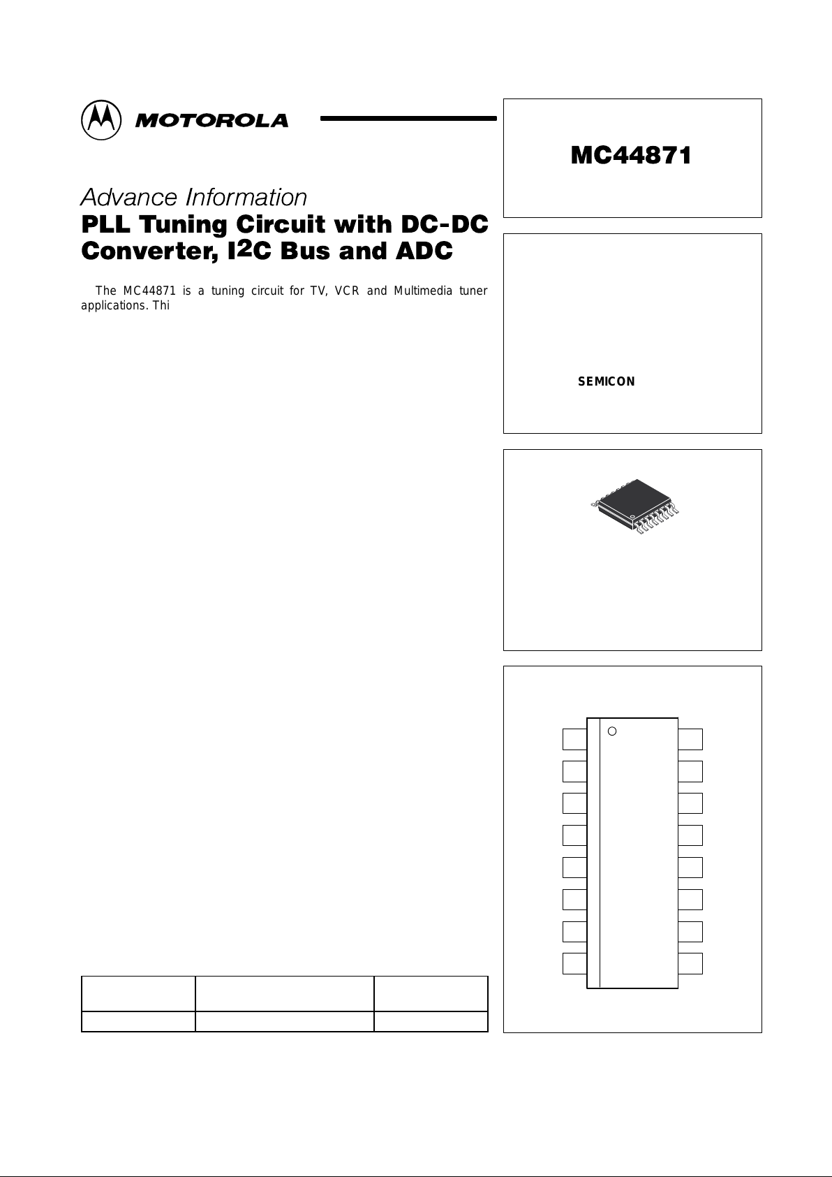
PIN CONNECTIONS
(16 Pin TSSOP)
Order this document by MC44871/D
116
15
14
13
12
11
10
9
2
3
4
5
6
7
8
V
TUN
CP
HF1
B2
B1
B0
Amp In
B4
DTB SUFFIX
PLASTIC PACKAGE
CASE 948F
(TSSOP–16)
16
1
HF2
Gnd
Xtal
SCL
SDA
ADD
V
CC
ADC
(Top View)
WITH HIGH SPEED I2C BUS
AND 30 V TUNING SUPPLY
1
MOTOROLA ANALOG IC DEVICE DATA
The MC44871 is a tuning circuit for TV, VCR and Multimedia tuner
applications. This device contains on one chip all the functions required for
PLL control of a VCO. This integrated circuit also contains a high frequency
prescaler and thus can handle frequencies up to 1.3 GHz.
The MC44871 has an integrated dc/dc converter to generate the 30 V
supply voltage for the tuning amplifier on the chip. A tuner using the
MC44871 does not require an external 30 V supply.
The MC44871 is controlled by a I2C bus, and has a chip address function.
The MC44871 data format is the same as the MC44818.
The MC44871 is manufactured on a single silicon chip using Motorola’s
high density bipolar process, MOSAIC (Motorola Oxide Self Aligned
Implanted Circuits).
• The Pin Called V
CC2
for the MC44818 is Now Called CP (Charge
Pump). This Pin is the Output of the DC/DC Converter; a 1.0 nF
Capacitor Replaces the Need for an External 30 V Supply
• High Speed I
2
C Bus (up to 800 kHz)
• I
2
C Bus Read Mode for Lock Detector and AFC Level
• HF Input is Balanced
• MC44871 has Three PNP High Current (30 mA) Band Buffers (B0, B1,
B2) and One NPN Low Current (5.0 mA) Band Buffer (B4)
• V
CC
Internally Supplies PNP Band Buffers
• The Tuning Voltage is Generated Through an External Pull–Up
Resistor (750 kΩ)
• Less Phase Comparator Output Current
• Single 5.0 V Supply Operation
MOSAIC is a trademark of Motorola, Inc.
ORDERING INFORMATION
Device
Operating
Temperature Range
Package
MC44871DTB TA = –20° to +85°C TSSOP–16
This document contains information on a new product. Specifications and information herein
are subject to change without notice.
Motorola, Inc. 1998 Rev 1

MC44871
2
MOTOROLA ANALOG IC DEVICE DATA
92
CP
687115.0 V
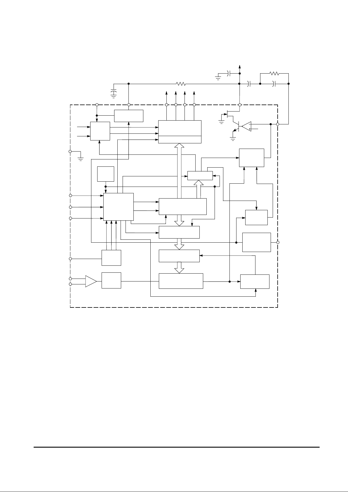
Figure 1. Representative Block Diagram
This device contains 3,204 active transistors.
Gnd
Test
Logic
Buffers
Latches
P–On
Reset
I2C Bus
Receiver
Latches
Phase
Comp
Ref
Divider
Latch Control
Program Divider
15 Bit
Latches B
Latches A
÷
8
Prescaler
Preamp
DTB2
POR
Operational
Amplifier
V
ref
DTB1
CLO
Data
RL
DTF
F
out
TDI
F
out
F
ref
T10, T11
T14
T13
4
6
15
1
F
out
F
ref
5
13
14
12
4
SDA
SCL
ADD
HF2
V
CC
V
TUN
Amp In
Xtal
B4 B2 B1 B0
DTS
512/1024
16
15
Shift Register
15 Bit
Approximate values of the external components for generation of the tuning voltage are:
C1 = 1.0 nF Charge Pump filter capacitor
R1 = 750 kΩ (560 kΩ minimum) Pull–up resistor
C4 = 330 pF V
TUN
filter capacitor
C2 = 47 nF, C3 = 22 nF, R2 = 39 kΩ Loop filter
These component values depend on the application.
ADC
10
ADC
3.2 or 4.0 MHz
Osc
3
HF1
C1
R1
C4
C3
R2
V
TUN
C2
Bands Out
DC/DC
Converter

MC44871
3
MOTOROLA ANALOG IC DEVICE DATA
MAXIMUM RATINGS (Maximum ratings are those values beyond which
permanent damage to the device may occur. Exposure to those limits may also affect device
reliability; TA = 25°C, unless otherwise noted.)
Rating
Pin Value Unit
Power Supply Voltage (VCC) 11 6.0 V
Storage Temperature – –65 to +150 °C
Operating Temperature Range – –20 to +85 °C
Operational Amplifier Output Voltage 1 40 V
RF Input Level 80 MHz to 1.3 GHz 3, 4 1.5 Vrms
NPN Band Buffer ”Off” Voltage 9 10 V
NPN Band Buffer ”On” Current 9 15 mA
PNP Band Buffer “Off” V oltage 6, 7, 8 6.0 V
PNP Band Buffer “On” Current 6, 7, 8 50 mA
PNP Band Buffer – Short Circuit Duration (Note 1) 6, 7, 8 Continuous –
Band Buffer Operation at 40 mA 6, 7, 8 10 s
all PNP Buffers “On”
NOTES: 1. At VCC = 5.0 V and TA = –20° to +80°C one buffer “On” only.
2.ESD data available upon request.
ELECTRICAL CHARACTERISTICS (Parameter Type: A–100% Tested, B–100% Correlation T ested, C–Characterized on
Samples, D–Design Parameter, VCC = 5.0 V , TA = 25°C, unless otherwise specified, 750 kΩ pull–up resistor between CP [Pin2] and
V
TUN
[Pin 1].)
Characteristic
Pin Min Typ Max Unit Type
VCC Supply Voltage Range 11 4.5 5.0 5.5 V A
VCC Supply Current (All Buffers “Off”)
– 35 45
A
One Buffer “On” when Open 11 – 40 50 mA B
One Buffer “On” at 40 mA – 80 90 B
PNP Band Buffer B0, B1, B2 Leakage Current when “Off” 6, 7, 8 – 0.01 1.0 µA A
PNP Band Buffer B0, B1, B2 Saturation Voltage when “On” at 30 mA 6, 7, 8 – 200 500 mV B
NPN Band Buffer B4 Leakage Current when “Off” 9 – 0.01 1.0 µA A
NPN Band Buffer ”Off” Voltage 9 0 – 5.5 V D
NPN Band Buffer B4 Saturation Voltage when “On” at 1.0 µA 9 – 50 100 mV A
NPN Band Buffer B4 Voltage when ”On” @ 5.0 mA 9 – 1.2 1.6 V A
Reference Oscillator Frequency Range 15 3.15 3.2 4.05 MHz D
Phase Comparator 3–State Current 16 –15 0 15 nA A
Phase Comparator Output Current – High Value 16 12 20 28 µA A
Phase Comparator Output Current – Low Value 16 2.0 6.0 10 µA A
DC–DC Converter Output Voltage, Sourcing 50 µA 2 28 31 34.5 V A
DC–DC Converter Maximum Current, Output Short Circuited 2 – 200 350 µA A
DC–DC Converter setting time from VCC >4.5 V to DC–DC Converter
Voltage > 28 V @ Load = 750 kΩ/1.0 nF
2 – – 25 ms C
Operational Amplifier Internal Reference Voltage (V
ref
) – 1.3 1.9 2.5 V A
Operational Amplifier Input Current 16 –15 0 15 nA A
Operational Amplifier DC Open Loop Gain – 100 300 – – A
Operational Amplifier Gain Bandwidth Product (CL = 1.0 nF) – 0.3 – – MHz D
Operational Amplifier Low Output Voltage, Sinking 50 µA 16 – 0.2 0.4 V D
Oscillator – Negative Resistance 15 1.0 – – kΩ D

MC44871
4
MOTOROLA ANALOG IC DEVICE DATA
PIN FUNCTION DESCRIPTION (see Figure 1)
Pin Symbol Description
1 V
TUN
Operational amplifier output which provides the tuning voltage
2 CP DC–DC Converter output (Charge Pump)
3, 4 HF1, HF2 Symmetrical HF inputs
5 Gnd Ground
6, 7, 8 B2, B1, B0 PNP Band Buffer outputs
9 B4 NPN Band Buffer output
10 ADC Three bit ADC for Automatic Frequency Tuning, readable through the bus
11 V
CC
Positive supply of the circuit (5.0 V)
12 ADD Chip address function
13 SDA I2C bus Data Input/Output
14 SCL I2C bus Clock
15 Xtal Crystal Oscillator (3.2 MHz or 4.0 MHz)
16 Amp In Operational amplifier input
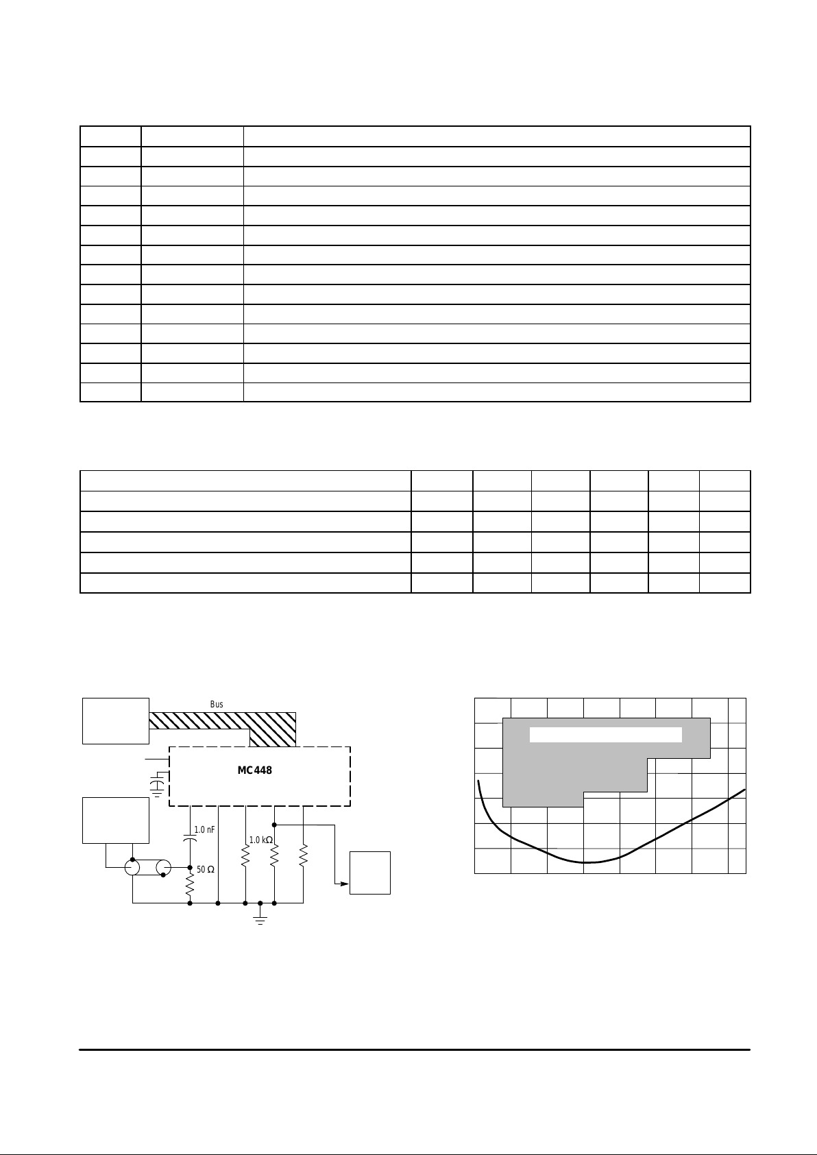
HF INPUT SENSITIVITY AND OVERLOAD CHARACTERISTICS (V
CC
= 5.0 V , TA = 25°C.) (See Figure 2.)
Characteristics
Pin Min Typ Max Unit Type
DC Bias (Internal) 3, 4 – 1.6 – V A
80–150 MHz 3, 4 10 – 315 mVrms C
150–600 MHz 3, 4 5.0 – 315 mVrms C
600–950 MHz 3, 4 10 – 315 mVrms C
950–1300 MHz 3, 4 50 – 315 mVrms C
50 Ω Cable
Figure 2. HF Sensitivity Test Circuit
NOTE: 1.Device is in test mode. B1, B2 are “On” and B0, B4 are “Off”.
Sensitivity is level of HF generator on 50 Ω load.
13 14
HF13Gnd5B08B17B26B4
9
Bus Controller
HF Generator
HF Out Gnd
11VCC = 5.0 V
Counter
In
Bus
1.0 k
Ω
50
Ω
1.0 nF
MC44871
4
1.0 nF
1.0 k
Ω
1.0 k
Ω
Guaranteed Sensitivity Performance
RF LEVEL (dBm)
FREQUENCY (MHz)
Figure 3. Typical HF Sensitivity Performance
(VCC = 5.0 V, Temperature = 25°C)
10
0
–10
–20
–30
–40
–50
–60
0 200 400 600 800 1000 1200 1400
 Loading...