

Motorola MC44864M Datasheet
PLL TUNING CIRCUIT
WITH 1.3 GHz PRESCALER
AND D/A CONVERTERS
PIN CONNECTIONS
Order this document by MC44864/D
M SUFFIX
PLASTIC PACKAGE
CASE 967
(EIAJ–20)
20
1
8
V
TUN
18
17
16
15
14
13
12
3
4
5
6
7
9
Amp In
V
CC2
DA2
DA3
V
CC1
Gnd
DA1
SCL
B
7
B
5
B
3
B
1
CA
(Top View)
20
19
1
2
XTAL
PHO
Gnd
SDA
1110
HF
1
HF
2
SEMICONDUCTOR
TECHNICAL DATA
Device
Operating
Temperature Range
Package
ORDERING INFORMATION
MC44864M TA = 0° to +70°C EIAJ–20
1
MOTOROLA ANALOG IC DEVICE DATA
! ! #
$
" !
!
The MC44864 is a tuning circuit for TV applications. This device contains
a PLL section and a DAC section and is MCU controlled through an I2C Bus.
The PLL section contains all the functions required to control the VCO of a
TV tuner. The IC generates the tuning voltage and the additional control
signals, such as band switching voltages.
The D/A section generates three additional varactor voltages to feed all of
the varactors of the tuner with individually optimized control voltages
(automatic tuner adjustment). The MC44864 is manufactured on a single
silicon chip using Motorola’s high density bipolar process, MOSIAC
(Motorola Oxide Self–Aligned Implanted Circuits).
• Complete Single Chip System for MPU Control
• Selectable ÷8 Prescaler Accepts Frequencies up to 1.3 GHz
• 15 Bit Programmable Divider Accepts Input Frequencies up to 165 MHz
• Programmable Reference Divider
• 3–State Phase/Frequency Comparator
• Operational Amplifier for Direct V aractor Control with Low Saturation
Voltage
• Four Output Buffers (15 mA)
• Output Options for 62.5 kHz, Reference Frequency and the
Programmable Divider
• The HF Input is Symmetrical
• Three 6 Bit DACs for Automatic Tuner Adjustment Allowing Use of
Non–Matched Varactors
• Better Tuner Performances Through Optimum Filter Response
• I
2
C Bus Controlled
• Four Chip Addresses for the PLL Section
• Four Chip Addresses for the D/A Section
• ESD Protected to MIL–STD–883C, Method 3015.7
(2,000 V, 1.5 kΩ, 150 pF)
MOSAIC is a trademark of Motorola, Inc.
MAXIMUM RATINGS (T
A
= 25°C, unless otherwise noted.)
Rating Pin Value Unit
Power Supply Voltage (V
CC1
) 9 6.0 V
Band Buffer “Off” Voltage 14 – 17 15 V
Band Buffer “On” Current 14 – 17 20 mA
Operational Amplifier Power Supply
Voltage (V
CC2
)
4 36 V
Operational Amplifier Short Circuit Duration
(0 to V
CC2
)
5 – 8 Continuous S
Storage Temperature – –65 to +150 °C
Operating Temperature Range – 0 to +70 °C
NOTE: ESD data available upon request.
Motorola, Inc. 1996 Rev 2
MC44864
2
MOTOROLA ANALOG IC DEVICE DATA
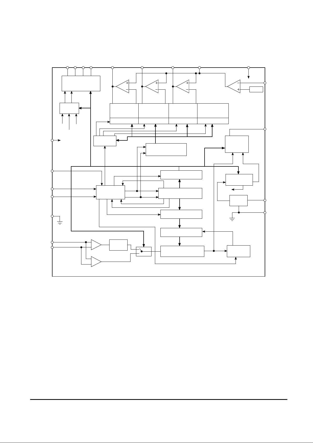
Representative Block Diagram
HF
1
HF
2
SCL
SDA
V
CC1
5.0 V
CA
V
CC2
33 V
Amp
In
XTAL
Gnd
Gnd
DA3 DA2 DA1 V
TUN
PHO
18
19
Buffers
Test
Logic
Bias
D/A 3
6 Bit
D/A 2
6 Bit
D/A 1
6 Bit
Ref
Voltage
Decoder
Shift Register
8 Bit
Phase
Comp
Latches
Shift Register
15 Bit
Latches A
Latches B
Program Divider
15 Bit
Latch
Control
I2C Bus
Receiver
÷
8
Presc
Preamp 1
Preamp 2
F
out
Ref
Divider
4.0 MHz
Osc
F1
62.5 kHz
TDI
F
ref
F
out
DTC
DTB
FUN
CL
Data
AD1
AD2 DTF
AVA
10
F
outFref
F1
8
Amp 4 Amp 3 Amp 2
3
9
13
4
12
1
20
765
11
2
Amp 1
Latches Latches Latches Latches
B7B5B3B
1
B7B5B3B
1
17 16 15 14
This device contains 3,551 active transistors.
MC44864
3
MOTOROLA ANALOG IC DEVICE DATA
ELECTRICAL CHARACTERISTICS (V
CC1
= 5.0 V , V
CC2
= 32 V, TA = 25°C, unless otherwise noted.)
Characteristic
Pin Min Typ Max Unit
V
CC1
Supply Voltage Range 9 4.5 5.0 5.5 V
V
CC1
Supply Current (V
CC1
= 5.0 V)
(1)(2)
9 – 50 70 mA
V
CC2
Supply Voltage Range 4 25 30 35 V
V
CC2
Supply Current (Output Open) 4 – 1.3 2.5
(4)
mA
Band Buffer Leakage Current when “Off” at 12 V 14 – 17 – 0.01 1.0 µA
Band Buffer Saturation Voltage when “On” at 15 mA 14 – 17 – 1.8 2.0 V
Data/Clock Current at 0 V 18, 19 –10 – 0 µA
Clock Current at 5.0 V 18 0 – 1.0 µA
Data Current at 5.0 V Acknowledge “Off” 19 0 – 1.0 µA
Data Saturation Voltage at 15 mA Acknowledge “On” 19 – 1.2 – V
Data/Clock Input Voltage Low 18, 19 – – 1.5 V
Data/Clock Input Voltage High 18, 19 3.0 – – V
Clock Frequency Range 18 – – 100 kHz
Phase Detector Current in High Impedance State 2 –15 – 15 nA
Oscillator Frequency Range 1, 2 3.5 4.0 4.1 MHz
Phase Detector High–State Source Current (@ 1.5 V) 2 –2.5 – –0.5 mA
Phase Detector Low–State Sink Current (@ 4.0 V) 2 0.5 – 2.5 mA
Operational Amplifier Internal Reference Voltage – 2.0 2.5 3.0 V
Operational Amplifier Input Current 3 –15 – 15 nA
DC Open Loop Gain – 2000 – – V/V
Gain Bandwidth Product – – 0.2 – MHz
Phase Margin – – 50 – Deg.
V
out
Low, Sinking 50 µA 6 – 8 – 0.2 0.5 V
V
out
High, Sourcing 50 µA (V
CC2
– V
out
High) 6 – 8 – – 1.5 V
Tuning V oltage (DC) 5 – 8 – – 30 V
D/A Converters Step Size
(3)
6 – 8 0.5 – 1.5 LSB
D/A Converters Temperature Drift 6 – 8 – 1.0 – LSB
DAC Offset at V
TUN
= 2.5 V – –50 – 50 mV
DAC Offset at V
TUN
= 25 V – –700 – 700 mV
DAC Voltages (DC) 6 – 8 – – 33 V
NOTES: 1. When prescaler “Off”, typical supply current is decreased by 10 mA.
2.Band Buffers “Off”, 2.4 mA more when one buffer is on.
3.For definition of the LSB, see Figure 9 in the D/A section.
4.2.5 mA as long as the analog outputs are not in saturation high, which means V
TUN
, V
DAC
(Pins 5, 6, 7, 8) lower than V
CC2
– 1.5 V. When all
outputs are in saturation high the maximum V
CC2
current is 5.0 mA.
MC44864
4
MOTOROLA ANALOG IC DEVICE DATA
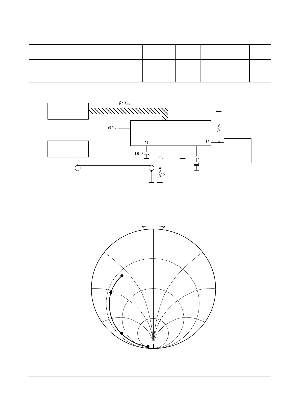
HF CHARACTERISTICS (See Figure 1)
Characteristic
Pin Min Typ Max Unit
DC Bias 10, 11 – 1.55 – V
Input Voltage Range mVrms
10–150 MHz (Prescaler “Off”) 10, 1 1 20 – 315
80–1000 MHz 10, 11 20 – 315
1000–1300 MHz 10, 11 50 – 315
50 Ω Cable
Figure 1. HF Sensitivity Test Circuit
MC44864
Device is in test mode: B7 is “On”, R2 = 1 and R3 = 0 (see Bus section).
Sensitivity is the level of the HF generator on 50 Ω load (without MC44864 load).
18, 19
10 12 1
Bus Controller
HF Generator
HF Out Gnd
9
V
CC1
Frequency
Counter
In
I2C Bus
1.0 nF
11
+5.0 V
17
50
Ω
4.0 MHz
22 pF
1.0 nF
3.9 k
B
7
12 V
–j +j
2
0.5
1
0.5
1
2
0.5
1
2
Figure 2. Typical HF Input Impedance
ZO = 50
Ω
500 MHz
1.3 GHz
1.0 GHz
50 MHz
0
 Loading...