

Motorola MC44827BDTB, MC44827DTB Datasheet
SEMICONDUCTOR
TECHNICAL DATA
LOW–POWER
PLL TUNING CIRCUIT
PIN CONNECTIONS
Order this document by MC44827/D
116
15
14
13
12
11
10
9
2
3
4
5
6
7
8
DA
CL
XTAL
V
CC2
33 V
V
CC1
5.0 V
HF In
EN
Gnd
DTB SUFFIX
PLASTIC PACKAGE
CASE 948F
(TSSOP–16)
16
1
Amp In
V
TUN
Lock
V
CC3
12 V
B3
B2
B1
B0
(Top View)
FOR 3–WIRE BUS WITH
1.3 GHz PRESCALER
1
MOTOROLA ANALOG IC DEVICE DATA
The MC44827/27B are tuning circuits for TV and VCR tuner applications.
They contain on one chip all the functions required for PLL control of a VCO.
The integrated circuits also contain a high frequency prescaler and thus can
handle frequencies up to 1.3 GHz.
The MC44827 has programmable 512/1024 reference divider while the
MC44827B has a fixed reference divider of 1024.
The MC44827/27B offer the same features as MC44817/17B but has
improved sensitivity performance and reduced power dissipation. The low
frequency preamplifier has been removed and the operational amplifier
pull–up resistor has been increased to 60 kΩ.
The MC44827/27B are controlled via a 3–wire bus. The MC44827/27B
have the same functions as the MC44828 which is I2C bus controlled. The
MC44827/27B and the MC44828 can be exchanged to allow conversion
between 3–wire bus and I2C bus control.
The MC44827/27B are manufactured on a single silicon chip using
Motorola’s high density bipolar process, MOSAIC (Motorola Oxide Self
Aligned Implanted Circuits).
• Complete Single Chip System for MPU Control (3–Wire Bus). Data and
Clock Inputs are I2C Bus Compatible
• Divide–by–8 Prescaler Accepts Frequencies up to 1.3 GHz
• 15 Bit Programmable Divider Accepts Input Frequencies up to 165 MHz
• 3–State Phase/Frequency Comparator
• Operational Amplifier for Direct Tuning Voltage Output (30 V)
• Four Integrated PNP Band Buffers can drive up to 40 mA
(V
CC1
to 14.4 V)
• Output Options for the Reference Frequency and the
Programmable Divider
• Bus Protocol for 18 or 19 Bit Transmission
• Extra 34–Bit Protocol for Test and Further Features
• High Sensitivity Preamplifier
• Lower Power Consumption, 200 mW Typical
• Improved Prescaler with Higher Margins for Sensitivity and
Temperature Range
• Lock Detector with Push–Pull Output
• Space–Saving TSSOP Package
• ESD Protected to MIL–STD–883C, Method 3015.7 (1.5 kΩ,100 pF)
MOSAIC is a trademark of Motorola, Inc.
ORDERING INFORMATION
Device
Operating
Temperature Range
Package
MC44827DTB
°
°
MC44827BDTB
T
A
= –
20° t
o +
80°C
TSSOP–16
Motorola, Inc. 1998 Rev 1
MC44827/27B
2
MOTOROLA ANALOG IC DEVICE DATA
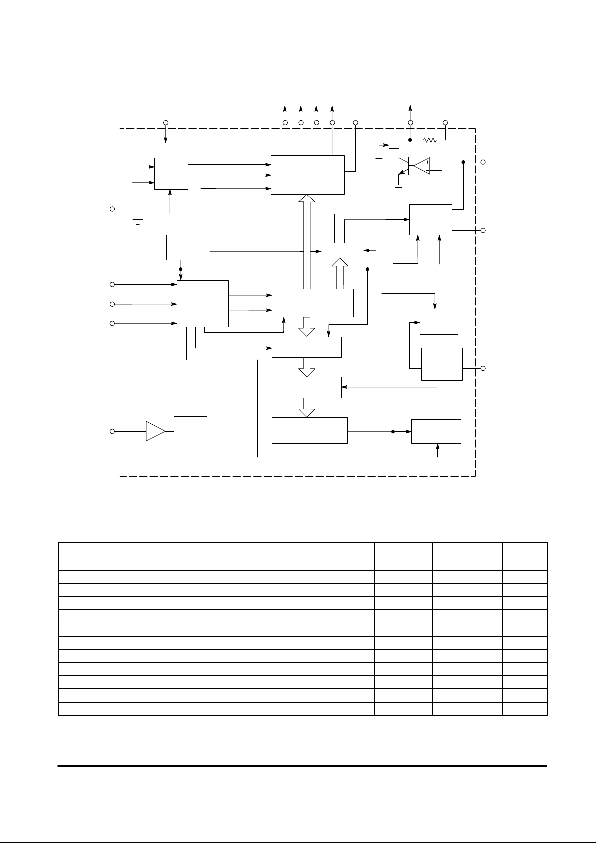
Figure 1. Representative Block Diagram
This device contains 3,204 active transistors.
Gnd
Test
Logic
Buffers
Latches
P–On
Reset
3–Wire Bus
Receiver
Latches
Phase
Comp
Ref
Divider
Osc
Latch Control
Program Divider
15 Bit
Latches B
Latches A
÷
8
Prescaler
Preamp 1
DTB2
POR
Operational
Amplifier
V
ref
60 k (1)
DTB1
CL
Data
RL
DTF
F
out
TDI
F
out
F
ref
T5
T0
…
T2
T4
4
6
15
10111213 14 5 675.0 V
F
out
F
ref
9
16
1
2
8
EN
DA
CL
HF In
V
CC1
V
CC3
12 V
V
TUN
V
CC2 33 V
Amp In
Lock
XTAL
B3 B2 B1 B0
DTS, EN
512/1024
B = 1024 Only
4
15
3
12 V
NOTE: 1. This part may be used with an external pull–up resistor of 20 kΩ to remain compatible with MC44817/17B
designed tuners. Pin 6 is left open. The internal pull–up can also be used with an external resistor in parallel.
Shift Register
15 Bit
MAXIMUM RATINGS (T
A
= 25°C, unless otherwise noted.)
Rating
Pin Value Unit
Power Supply Voltage (V
CC1
) 7 6.0 V
Band Buffer “Off” Voltage 10–13 14.4 V
Band Buffer “On” Current 10–13 50 mA
Band Buffer Pin Shorted to Ground or V
CC3
(Short Circuit Duration) (Note 1) 10–13 Continuous –
Operational Amplifier Power Supply Voltage (V
CC2
) 6 40 V
Operational Amplifier Pin Shorted to Ground or V
CC2
(Short Circuit Duration) 5 Continuous –
Power Supply Voltage (V
CC3
) 14 14.4 V
Storage Temperature – –65 to +150 °C
Operating Temperature Range – –20 to +80 °C
Band Buffer Operation (Note 2) at 50 mA each Buffer All Buffers “On” Simultaneously 10–13 10 s
Operational Amplifier Output Voltage 5 V
CC2
V
RF Input Level (80 MHz to 1.3 GHz) 8 1.5 Vrms
NOTES: 1. At V
CC3
= V
CC1
to 14.4 V and TA = –20° to +80°C one buffer “On” only.
2.At V
CC3
= V
CC1
to 14.4 V and TA = –20° to +80°C.
3.ESD data available upon request.
MC44827/27B
3
MOTOROLA ANALOG IC DEVICE DATA
ELECTRICAL CHARACTERISTICS (Parameter Type: A–100% Tested, B–100% Correlation Tested, C–Characterized on Samples,
D–Design Parameter. V
CC1
= 5.0 V; V
CC2
= 33 V; V
CC3
= 12 V; TA = 25°C, unless otherwise noted.)
Characteristic
Pin Min Typ Max Unit Type
V
CC1
Supply Voltage Range 7 4.5 5.0 5.5 V A
V
CC2
Supply Voltage Range 6 25 32 37 V A
V
CC3
Supply Voltage Range 14 V
CC1
12 14.4 V A
V
CC1
Supply Current (V
CC1
= 5.0 V; V
CC3
= 12 V) One Buffer “On” 7 – 23 30 mA A
V
CC2
Supply Current (Output Open) V
TUN
= 15 V 6 – 0.3 1.0 mA A
V
CC3
Supply Current 14 mA A
All Buffers “Off” – 0.15 0.3
One Buffer “On” when Open – 6.5 8.0
One Buffer “On” at 40 mA – 46.5 50
Band Buffer Leakage Current when “Off” at 12 V 10–13 – 0.01 1.0 µA A
Band Buffer Saturation Voltage when “On” at 30 mA 10–13 – 0.15 0.3 V B
Band Buffer Saturation Voltage when “On” at 40 mA 10–13 – 0.2 0.5 V A
Data/Clock/Enable Current at 0 V 1, 2, 16 –10 – 0 µA A
Data/Clock/Enable Current at 5.0 V 1, 2, 16 0 – 1.0 µA A
Data/Clock/Enable Input Voltage Low 1, 2, 16 – – 1.5 V A
Data/Clock/Enable Input Voltage High 1, 2, 16 3.0 – – V A
Clock Frequency Range 2 – – 100 kHz D
Oscillator Frequency Range 3 3.15 3.2 4.05 MHz D
Operational Amplifier Internal Reference Voltage – 1.8 2.75 3.5 V A
Operational Amplifier Input Current 4 –15 0 15 nA A
DC Open Loop Gain – 100 250 – – B
Gain Bandwidth Product (CL = 1.0 nF) – 0.3 – – MHz C
V
out
Low, Sinking 50 µA (Note 1) 5 – 80 200 mV A
V
out
High, Sourcing 3.0 µA, V
CC2
– V
out
5 – 0.2 0.5 V B
Phase Comparator 3–State Current 4 –15 0 15 nA A
Charge Pump High Current of Phase Comparator 4 30 50 85 µA A
Charge Pump Low Current of Phase Comparator 4 10 15 30 µA A
NOTE: 1. Using the internal 60 kΩ pull–up resistor only.
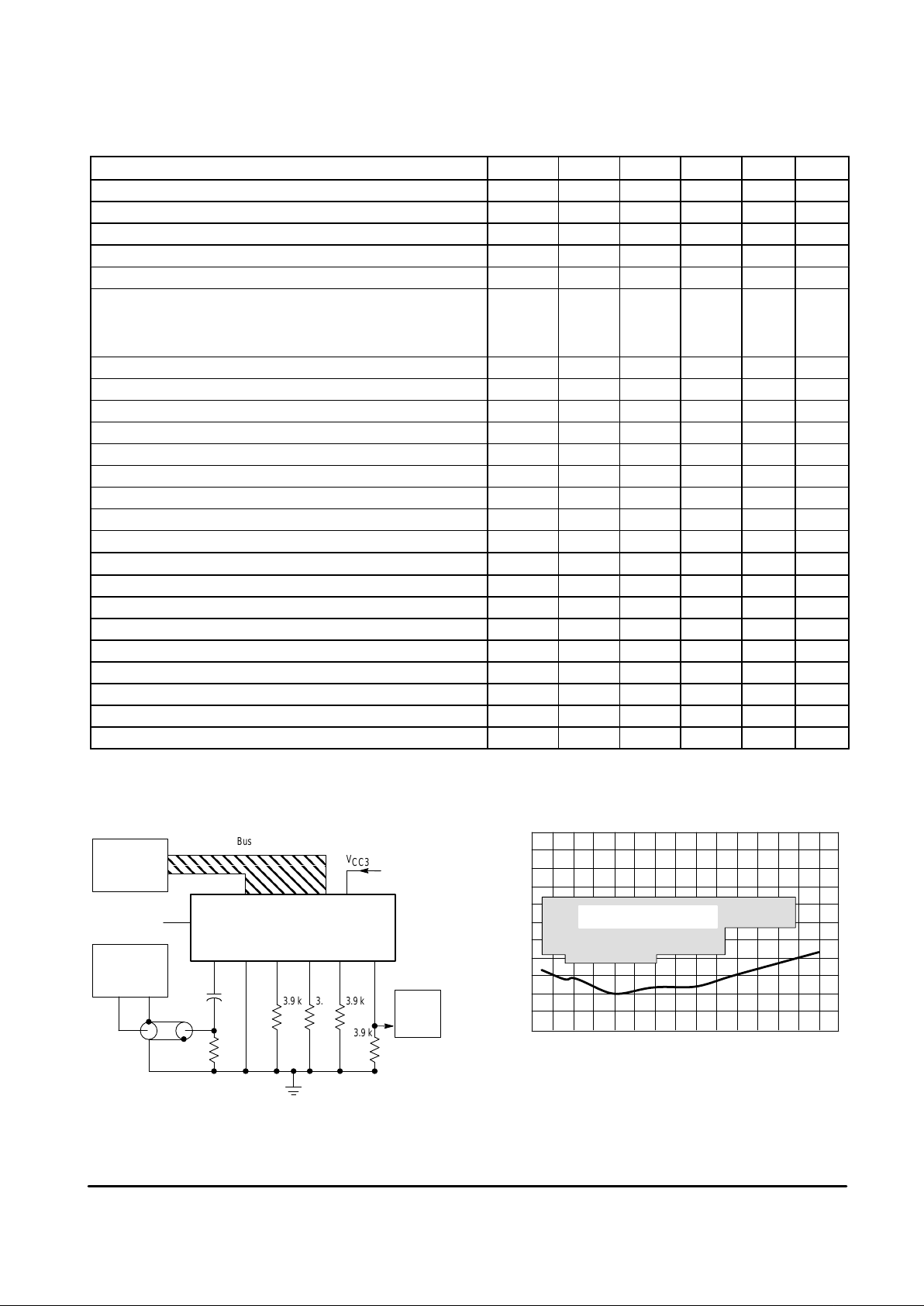
Figure 2. HF (Prescaler Input) Sensitivity Test Circuit
NOTES: 1.Device is in test mode. B2, B3 are “On” and B0, B1 are “Off”.
2.Sensitivity is level of HF generator on 50 Ω load.
16 1 2 14
HF8Gnd9B010B111B212B3
13
Bus Controller
HF Generator
HF Out Gnd
7V
CC1
Counter
In
V
CC3
Bus
3.9 k
3.9 k3.9 k 3.9 k
50
Ω
50 Ω Cable
1.0 nF
MC44827/27B
Guaranteed Operating Area
0
40
RF Level (dBm)
RF In (MHz)
200 400
600
800 1000 1200 1400
20
0
–20
–40
–60
Figure 3. Typical Prescaler Input Sensitivity
 Loading...