

Motorola MC44824D, MC44825D Datasheet
7
SDA
6
XTAL2
14
TV AND VCR
PLL TUNING CIRCUITS
WITH 1.3 GHz PRESCALER
AND I2C BUS
PIN CONNECTIONS
Order this document by MC44824/D
116
15
14
13
12
11
10
9
2
3
4
5
6
8
PD
XTAL1
XTAL2
B
7
B
4
CA
UD
B
2
D SUFFIX
PLASTIC PACKAGE
CASE 751B
(SO–16)
16
1
SCL
GND
HF2
HF1
V
CC
B
0
B
1
(Top View)
14
1
D SUFFIX
PLASTIC PACKAGE
CASE 751A
(SO–14)
13
12
11
10
9
8
1
2
3
4
5
7
PD
XTAL1
SCL
B
7
CA B
2
SDA
UD
GND
HF2
HF1
V
CC
B
1
(Top View)
MC44824
MC44825
1
MOTOROLA ANALOG IC DEVICE DATA
The MC44824/25 are tuning circuits for TV and VCR tuner applications.
They contain on one chip all the functions required for PLL control of a VCO.
The integrated circuits also contain a high frequency prescaler and thus can
handle frequencies up to 1.3 GHz.
The MC44824/25 are manufactured on a single silicon chip using
Motorola’s high density bipolar process, MOSAIC (Motorola Oxide Self
Aligned Implanted Circuits).
• Complete Single Chip System for MPU Control (I
2
C Bus). Data and
Clock Inputs are 3–Wire Bus Compatible
• Divide–by–8 Prescaler Accepts Frequencies up to 1.3 GHz
• 15 Bit Programmable Divider
• Reference Divider: Programmable for Division Ratios 512 and 1024
• 3–State Phase/Frequency Comparator
• 4 Programmable Chip Addresses
• 3 Output Buffers (MC44824) respectively 5 Output Buffers (MC44825)
for 10 mA/15 V
• Operational Amplifier for use with External NPN Transistor
• SO–14 Package for MC44824 and SO–16 for MC44825
• High Sensitivity Preamplifier
• Fully ESD Protected
MOSAIC is a trademark of Motorola, Inc.
ORDERING INFORMATION
Device
Operating
Temperature Range
Package
MC44824D
°
°
SO–14
MC44825D
T
A
= –
20° t
o +
80°C
SO–16
Motorola, Inc. 1996 Rev 1
MC44824/25
2
MOTOROLA ANALOG IC DEVICE DATA
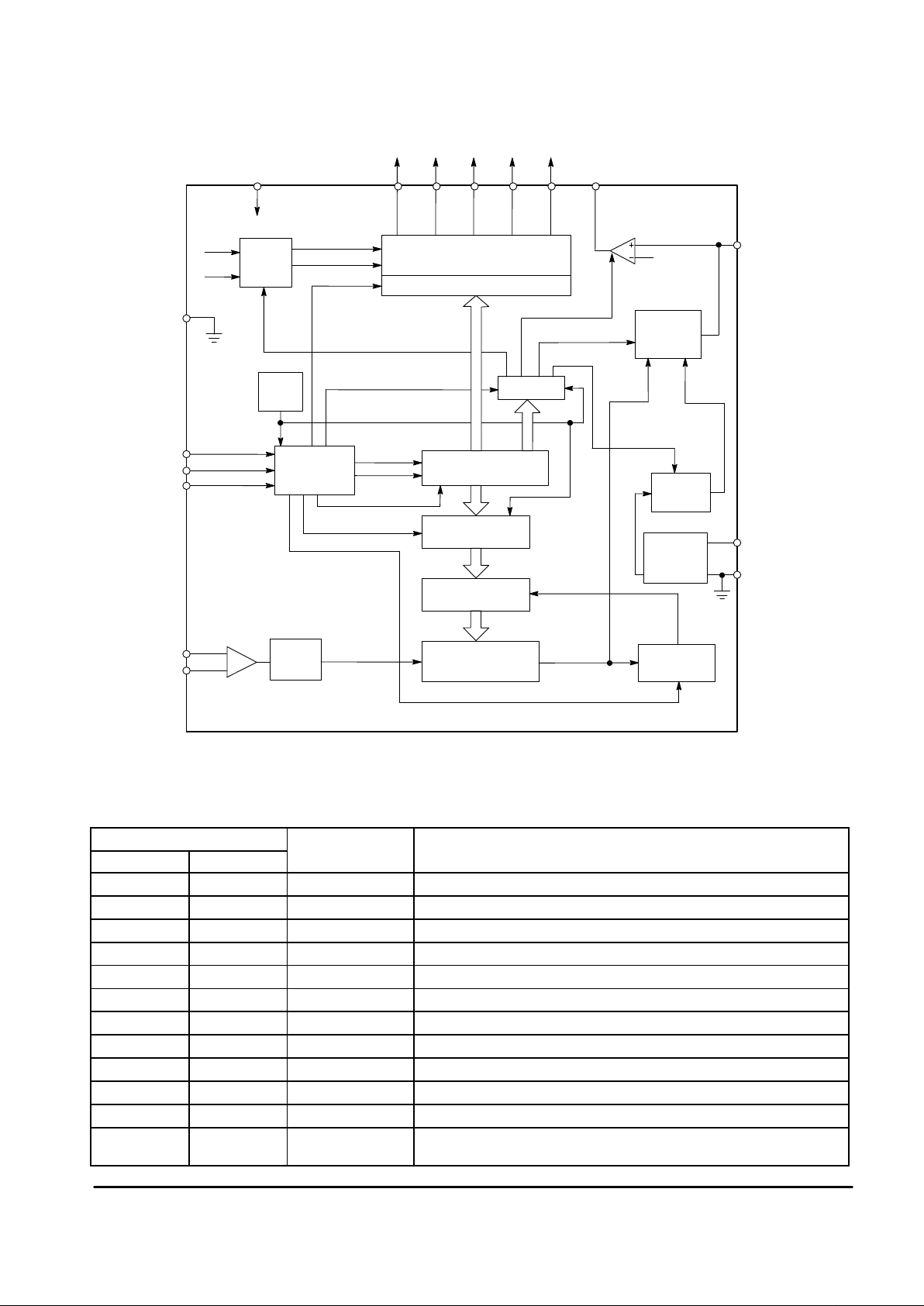
Representative Block Diagram
This device contains 3,204 active transistors.
Gnd
Test
Logic
Buffers
Latches
P–On
Reset
I2C Bus
Receiver
Latches
Phase
Comp
Ref
Divider
3.2 or 4.0
MHz Osc
Latch Control
Program Divider
15 Bit
Latches B
Latches A
Shift Register
15 Bit
÷
8
Prescaler
Preamp
DTB2
POR
Operational
Amplifier
2.7 V
DTB1
CL
Data
RL
DTF
F
out
TDI
F
out
F
ref
T10, T
11
T9, T12, T
14
T
13
T
8
4
7
9
(10)
8
(9)(7)
6
(6)
14
(16)
10
(12)
5.0 V
F
out
F
ref
13 (15)
7 (8)
4 (4)
5 (5)
11 (13)
CA
SDA
SCL
HF Input1
V
CC
UD
PD
XTAL2
B
7
B
4
B2B
1
DTS, EN
512/1024
1 (1)
3 (3)
12 (14)
HF Input2
XTAL1
2 (2)
Gnd
(11)
B
0
MC44825 Pin Numbers ( )
PIN FUNCTION DESCRIPTION
Pin
MC44824 MC44825
Symbol Description
1 1 PD Input of tuning voltage amplifier
2 2 XTAL1 First crystal input is the active pin at the oscillators
3 3 XTAL2 Second crystal input is the internal ground
4 4 SDA Data input
5 5 SCL Clock input of the I2C bus
6, 8, 9 – B7, B2, B
1
Band buffer (open collector) outputs for up to 10 mA
– 6, 7, 9, 10, 11 B7, B4, B2, B1, B
0
Band buffer (open collector) outputs for up to 10 mA
7 8 CA Chip address selection pin
10 12 V
CC
Supply voltage, typical 5.0 V
11, 12 13, 14 HF1/HF2 Symmetric HF inputs from local oscillator
13 15 GND Ground
14 16 UD Output of the tuning voltage amplifier. Needs an external NPN with pull–up
resistor to drive the varicaps
MC44824/25
3
MOTOROLA ANALOG IC DEVICE DATA
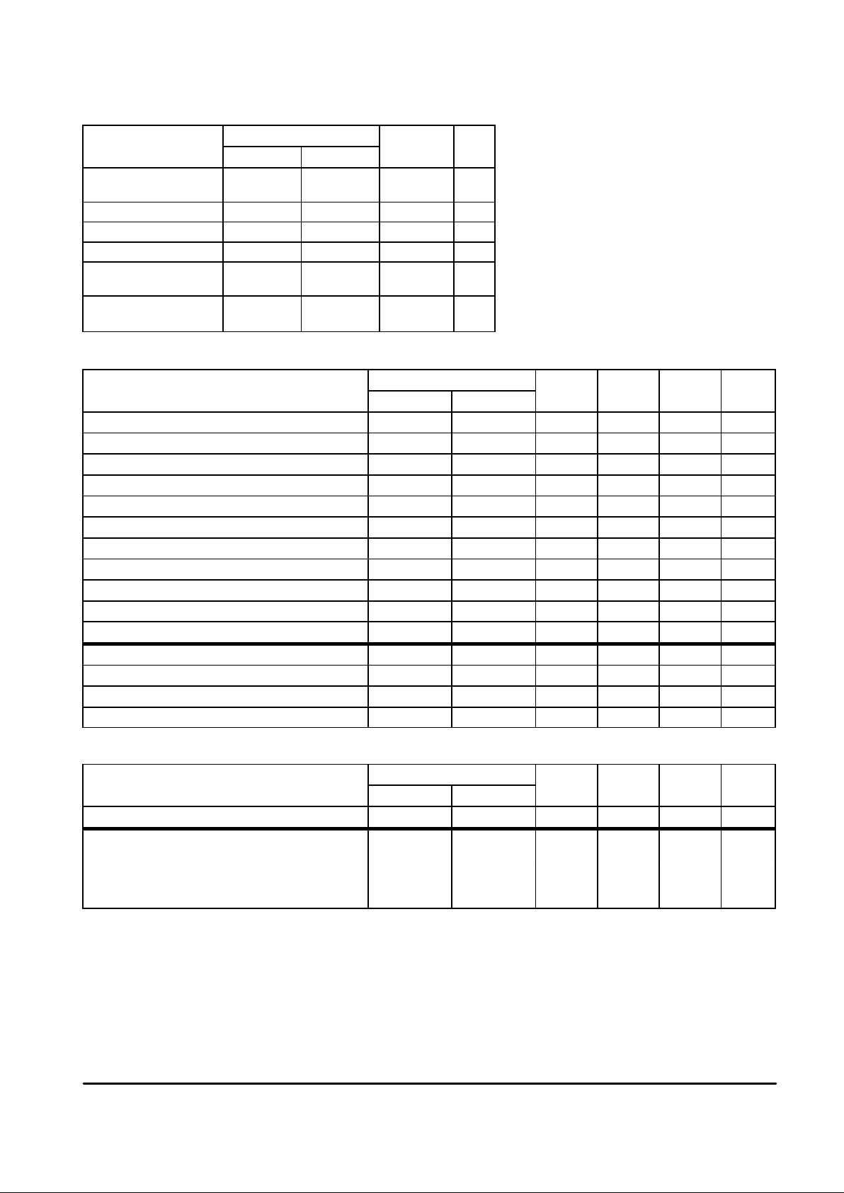
MAXIMUM RATINGS (T
A
= 25°C, unless otherwise noted.)
Pin
Rating
MC44824 MC44825
Value Unit
Power Supply Voltage
(VCC)
10 12 6.0 V
Band Buffer “Off” Voltage 6, 8, 9 6, 7, 9, 10, 11 15 V
Band Buffer “On” Current 6, 8, 9 6, 7, 9, 10, 11 15 mA
Storage Temperature – – –65 to +150 ° C
Operating Temperature
Range
– – –20 to +80 °C
RF Input Level (10 MHz
to 1.3 GHz)
11, 12 13, 14 1.5 Vrms
ELECTRICAL CHARACTERISTICS (V
CC
= 5.0 V , TA = 25°C, unless otherwise noted.)
Pin
Characteristic
MC44824 MC44825
Min Typ Max Unit
VCC Supply Voltage Range 10 12 4.5 5.0 5.5 V
VCC Supply Current (VCC = 5.0 V) 10 12 – 40 55 mA
Band Buffer Leakage Current when “Off” at 12 V 6, 8, 9 6, 7, 9, 10, 11 – 0.01 1.0 µA
Band Buffer Saturation Voltage when “On” at 10 mA 6, 8, 9 6, 7, 9, 10, 11 – 1.6 1.8 V
Data Saturation Voltage at 15 mA Acknowledge “On” 4 4 – – 1.0 V
Data/Clock/Enable Current at 0 V 4, 5 4, 5 –10 – 0 µA
Data/Clock/Enable Current at 5.0 V 4, 5 4, 5 0 – 1.0 µA
Data/Clock/Enable Input Voltage Low 4, 5 4, 5 – – 1.5 V
Data/Clock/Enable Input Voltage High 4, 5 4, 5 3.0 – – V
Clock Frequency Range 5 5 – – 100 kHz
Oscillator Frequency Range 2, 3 2, 3 3.15 3.2 4.05 MHz
Operational Amplifier Input Current 1 1 –15 0 15 nA
Phase Detector Current in High Impedance State 1 1 –15 0 15 nA
Charge Pump Current of Phase Comparator, T14 = 0 1 1 30 40 60 µA
Charge Pump Current of Phase Comparator, T14 = 1 1 1 100 125 200 µA
HF CHARACTERISTICS (See Figure NO T AG)
Pin
Characteristic
MC44824 MC44825
Min Typ Max Unit
DC Bias 11, 12 13, 14 – 1.6 – V
Input Voltage Range mVrms
80–150 MHz 11, 12 13, 14 10 – 315
150–600 MHz 11, 12 13, 14 5.0 – 315
600–950 MHz 11, 12 13, 14 10 – 315
950–1300 MHz 11, 12 13, 14 50 – 315
 Loading...