

Motorola MC44817D, MC44817BD Datasheet
T
20° t
80°C
SO–16
Order this document by MC44817/D
The MC44817/17B are tuning circuits for TV and VCR tuner applications.
They contain on one chip all the functions required for PLL control of a VCO.
The integrated circuits also contain a high frequency prescaler and thus can
handle frequencies up to 1.3 GHz.
The MC44817 has programmable 512/1024 reference divider while the
MC44817B has a fixed reference divider of 1024.
The MC44817/17B are manufactured on a single silicon chip using
Motorola’s high density bipolar process, MOSAIC (Motorola Oxide Self
Aligned Implanted Circuits).
• Complete Single Chip System for MPU Control (3–Wire Bus). Data and
Clock Inputs are IIC Bus Compatible
• Divide–by–8 Prescaler Accepts Frequencies up to 1.3 GHz
• 15 Bit Programmable Divider Accepts Input Frequencies up to 165 MHz
• Reference Divider: Programmable for Division Ratios 512 and 1024.
The MC44817B has a Fixed 1024 Reference Divider
• Tri–State Phase/Frequency Comparator
• Operational Amplifier for Direct Tuning Voltage Output (30 V)
• Four Integrated PNP Band Buffers for 40 mA (V
• Output Options for the Reference Frequency and the
Programmable Divider
• Bus Protocol for 18 or 19 Bit Transmission
• Extra Protocol for 34 Bit for Test and Further Features
• High Sensitivity Preamplifier
• Circuit to Detect Phase Lock
• Fully ESD Protected
CC1
to 14.4 V)
TV AND VCR
PLL TUNING CIRCUITS
WITH 1.3 GHz PRESCALER
AND 3–WIRE BUS
SEMICONDUCTOR
TECHNICAL DATA
16
1
D SUFFIX
PLASTIC PACKAGE
CASE 751B
(SO–16)
PIN CONNECTIONS
MOSAIC is a trademark of Motorola, Inc.
ORDERING INFORMATION
Device
MC44817D
MC44817BD
MOTOROLA ANALOG IC DEVICE DATA
Operating
Temperature Range
= –
A
116
DA
CL
2
XTAL
3
Amp In
V
Package
°
°
o +
V
33 V
CC2
V
5.0 V
CC1
Motorola, Inc. 1996 Rev 1
TUN
HF In
4
5
6
7
8
(Top View)
15
14
13
12
11
10
EN
Lock
V
12 V
CC3
B
3
B
2
B
1
B
0
Gnd
9
1
Gnd
EN
Data
Clock
F
9
16
1
2
F
out
ref
V
CC1
Logic
Test
P–On
Reset
3–Wire Bus
Receiver
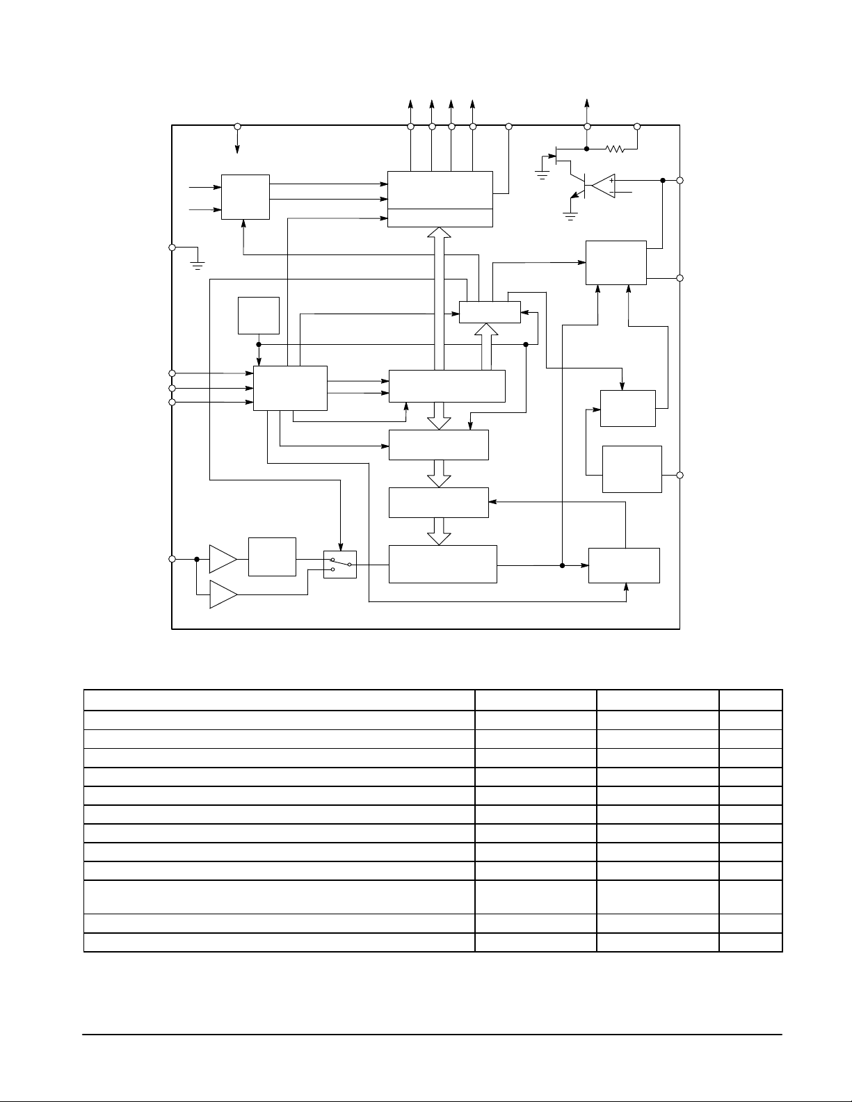
MC44817/17B
Representative Block Diagram
Bands Out 30 mA
°
(40 mA at 0
DTB1
DTB2
POR
CL
Data
RL
to 80°C)
B3B2B1B
Buffers
Latches
T
6
4
Shift Register
15 Bit
15
10111213 14 5 675.0 V
0
T
4
Latches
V
T0
6
CC3
…
12 V
T
V
TUN
V
CC2
20 k
4
Amp In
2.7 V
Operational
Amplifier
3
T
5
Phase
Comp
F
out
15
Lock
F
ref
512/1024
B = 1024 Only
Ref
Divider
DTF
Latches A
Latches B
TDI
Osc
3
XTAL
Preamp 1
÷
HF Input
8
Preamp 2
8
Prescaler
Program Divider
15 Bit
F
Latch Control
out
DTS, EN
This device contains 3,204 active transistors.
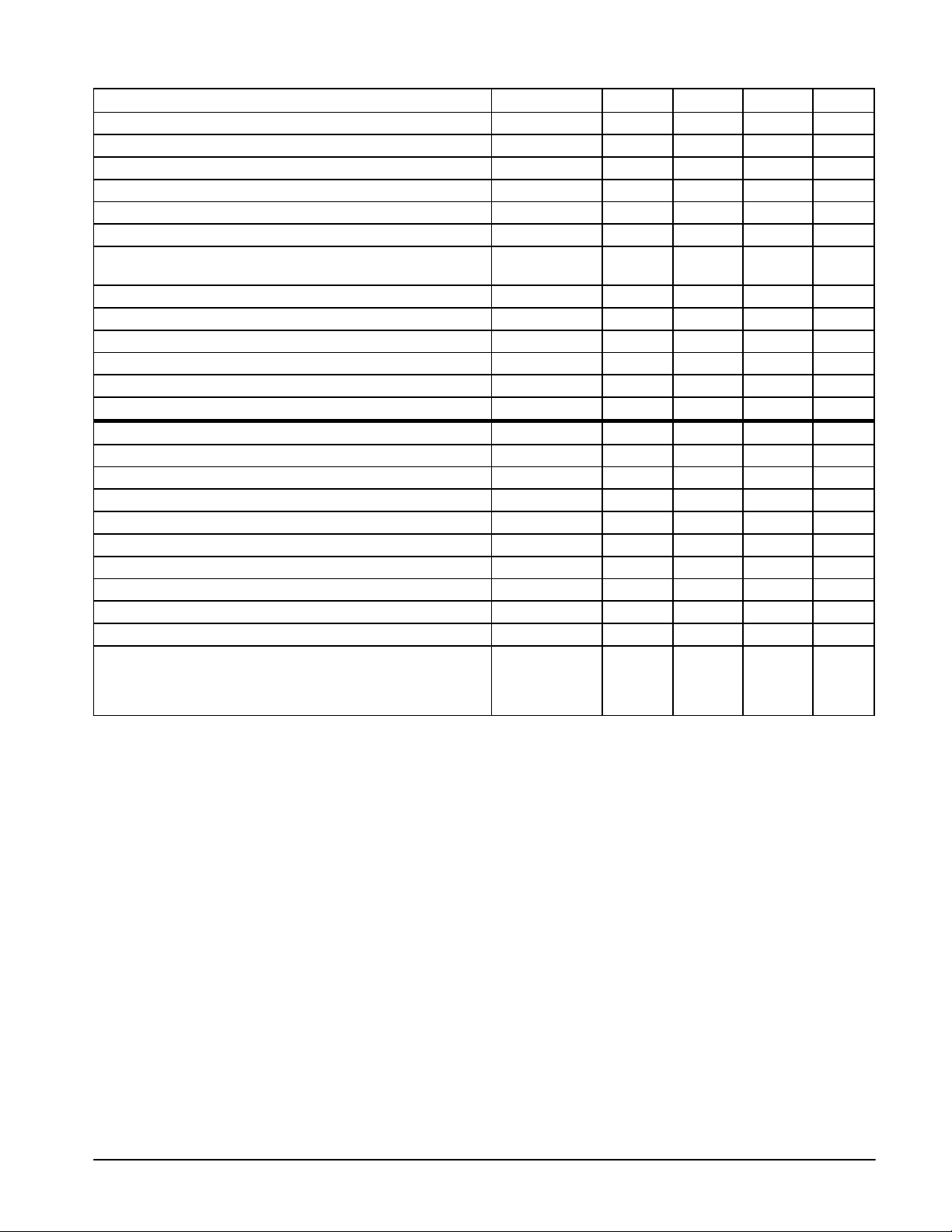
MAXIMUM RATINGS (T
= 25°C, unless otherwise noted.)
A
Rating Pin Value Unit
Power Supply Voltage (V
) 7 6.0 V
CC1
Band Buffer “Off” Voltage 10–13 14.4 V
Band Buffer “On” Current 10–13 50 mA
Band Buffer – Short Circuit Duration (0 to V
Operational Amplifier Power Supply Voltage (V
Operational Amplifier Short Circuit Duration (0 to V
Power Supply Voltage (V
) 14 14.4 V
CC3
) (Note 2) 10–13 Continuous –
CC3
) 6 40 V
CC2
) 5 Continuous –
CC2
Storage Temperature – –65 to +150 °C
Operating Temperature Range – –20 to +80 °C
Band Buffer Operation (Note 1) at 50 mA each Buffer
10–13 10 sec
All Buffers “On” Simultaneously
Operational Amplifier Output Voltage 5 V
CC2
RF Input Level (10 MHz to 1.3 GHz) – 1.5 Vrms
NOTES: 1. At V
2.At V
CC3
CC3
= V
to 14.4 V and TA = –20° to +80°C.
CC1
= V
to 14.4 V and TA = –20° to +80°C one buffer “On” only.
CC1
V
2
MOTOROLA ANALOG IC DEVICE DATA
MC44817/17B
ELECTRICAL CHARACTERISTICS (V
Characteristic
V
Supply Voltage Range 7 4.5 5.0 5.5 V
CC1
V
Supply Current (V
CC1
V
Supply Voltage Range 6 25 – 37 V
CC2
V
Supply Current (Output Open) 6 – 1.5 3.5 mA
CC2
Band Buffer Leakage Current when “Off” at 12 V 10–13 – 0.01 1.0 µA
Band Buffer Saturation Voltage when “On” at 30 mA 10–13 – 0.15 0.3 V
Band Buffer Saturation Voltage when “On” at 40 mA
only for 0° to 80°C
Data/Clock/Enable Current at 0 V 1, 2, 16 –10 – 0 µA
Data/Clock/Enable Current at 5.0 V 1, 2, 16 0 – 1.0 µA
Data/Clock/Enable Input Voltage Low 1, 2, 16 – – 1.5 V
Data/Clock/Enable Input Voltage High 1, 2, 16 3.0 – – V
Clock Frequency Range 2 – – 100 kHz
Oscillator Frequency Range 3 3.15 3.2 4.05 MHz
Operational Amplifier Internal Reference Voltage – 2.0 2.75 3.2 V
Operational Amplifier Input Current 4 –15 0 15 nA
DC Open Loop Voltage Gain – 100 250 – V/V
Gain Bandwidth Product (CL = 1.0 nF) – 0.3 – – MHz
V
Low, Sinking 50 µA 5 – 0.2 0.4 V
out
V
High, Sourcing 10 µA, V
out
Phase Comparator Tri–State Current 4 –15 0 15 nA
Charge Pump High Current of Phase Comparator 4 30 50 85 µA
Charge Pump Low Current of Phase Comparator 4 10 15 30 µA
V
Supply Voltage Range 14 V
CC3
V
Supply Current 14 mA
CC3
All Buffers “Off” – 0.2 0.5
One Buffer “On” when Open – 8.0 13
One Buffer “On” at 40 mA – 48 53
= 5.0 V) 7 – 37 50 mA
CC1
– V
CC2
out
CC1
= 5.0 V, V
CC2
= 33 V, V
= 12 V, TA = 25°C, unless otherwise noted.)
CC3
Pin Min Typ Max Unit
10–13 – 0.2 0.5 V
5 – 0.2 0.5 V
CC1
– 14.4 V
Data Format and Bus Receiver
The circuit is controlled by a 3–wire bus via Data (DA),
Clock (CL), and Enable (EN) inputs. The Data and Clock
inputs may be shared with other inputs on the IIC–Bus while
the Enable is a separate signal. The circuit is compatible with
18 and 19 bit data transmission and also has a mode for
34 bit transmission for test and additional features.
The 3–wire bus receiver receives data for the internal shift
register after the positive going edge of the EN–signal. The
data is transmitted to the band buffers on the negative going
edge of the clock pulse 4 (signal DTB1).
18 and 19 Bit Data Transmission
The programmable divider may receive 14 bit (18 bit
transmission) or 15 bit (19 bit transmission). The data is
transmitted to the programmable divider (latches A) on the
negative going edge of clock pulse 19 or on the negative
edge of the EN–signal if EN goes down after the 18th clock
pulse (signal DTF). If the programmable divider receives
14 bit, its MSB (bit N14) is internally reset. The reset pulse is
generated only if EN goes negative after the 18th clock pulse
(signal RL).
MOTOROLA ANALOG IC DEVICE DATA
34 Bit Data Transmission
(For Test and Additional Features)
In the test mode, the programmable divider receives 15 bit
and the data is transferred to latches A on the negative edge
of clock pulse 19 (signal DTF). The information for test is
received on clock pulses 20 to 26 and transmitted to the
latches on the negative edge of pulse 34 (signal DTB2).
These latches have a power–on reset. The power–on reset
sets the programmable divider to a counting ratio of 256 or
higher and resets the corresponding latches to the test bits
T0 to T6 (signal POR). The bus receiver is not disturbed if the
data format is wrong. Useless bits are ignored. If for example
the Enable signal goes low after the clock pulse 9, bits one to
four are accepted as valid buffer information and the other
bits are ignored. If more than 34 bits are received, bit 35 and
the following are ignored.
Lock Detector
The lock–detector output is low in lock. The output goes
immediately high when an unlock condition is detected. The
output goes low again when the loop is in lock during a
complete period of the reference frequency.
3
 Loading...