Motorola MC44725VFU Datasheet
MC44724/5 Rev 0.21 03/25/97
No.
This document contains information on a new product. Specifications and information herein are subject to change without notice.
1
Advance Information
Digital Video Encoder
RGB Output Support
HCMOS Technology
MC44724
MC44725
VFU SUFFIX
64 VQFP
(0.5mm Pitch)
The MC44724 and MC44725 are Digital Video Encoders (DVE).
They convert ITU-601/656 standard 4:2:2 Bit-Paralellel data into
analog composite video, S-Video or Y/Cb/Cr or R/G/B in PAL
and NTSC formats. They accept the multiplexed ((CB,Y,CR)Y)
signals from digital sources such as MPEG decoders and can act as
a sync generator master. All video processing is done digitally and
requires no external adjustment.
Specifically designed for digital satellite, digital cable decoders
and multimedia terminals.
• World Wide Operation (PAL-BDGHI, PAL-N,PAL-M, NTSC-M)
• SMPTE 170M / ITU - R 624 composite video output
• Programmable Color Sub-carrier Frequencies
• Analog Horizontal, Vertical, Frame or Composite Sync Outputs
• Sync Extraction From Digital Input Data (SAV, EAV)
• Sync Polarity and Horizontal Phase Control
• Master or Slave Sync (H/Vsync, H/Fsync, ITU-R656 Slave) Operation
• Interlaced or Non-Interlaced Support
• 625/50 or 525/60 ITU-601/656 two 8-bit or 16-bit ((CB,Y,CR)Y) Digital Input
• Luma 2X / Chroma 4X Oversampling Filtering
• External VBI Information Data Input (such as TeleText Information Data)
• Selectable Two sets of Signals within (CVBS/Y/C) or (Y/Cb/Cr) or (R/G/B)
• Six Analog Outputs Through 10-bit DACs
• Easily programmed via Serial Bus ( I2C or SPI Bus)
• 2 Hardware I2C Chip Addresses
• Closed-Caption, CGMS and WSS Information data Insertion
• MACROVISION ver. 7.01 Anti-Copy Signal Insertion(MC44724 Only)
• On Chip Color - bar Generator
• +3.3V Power Supply or +3.3V(Digital)/+5V(Analog) Power Supply
The MC44724 device is protected by U.S. patent number 4,631,603,4,577,216 and 4,819,098
and other intellectual property rights. The use of Macrovision's copy protection technology in the
device must be authorized by Macrovision and is intended for home and other limited pay-perview uses only, unless otherwise authorized in writing by Macrovision. Reverse engineering or
disassembly is prohibited.
MC44724/5 Rev 0.21 03/25/97
No.
This document contains information on a new product. Specifications and information herein are subject to change without notice.
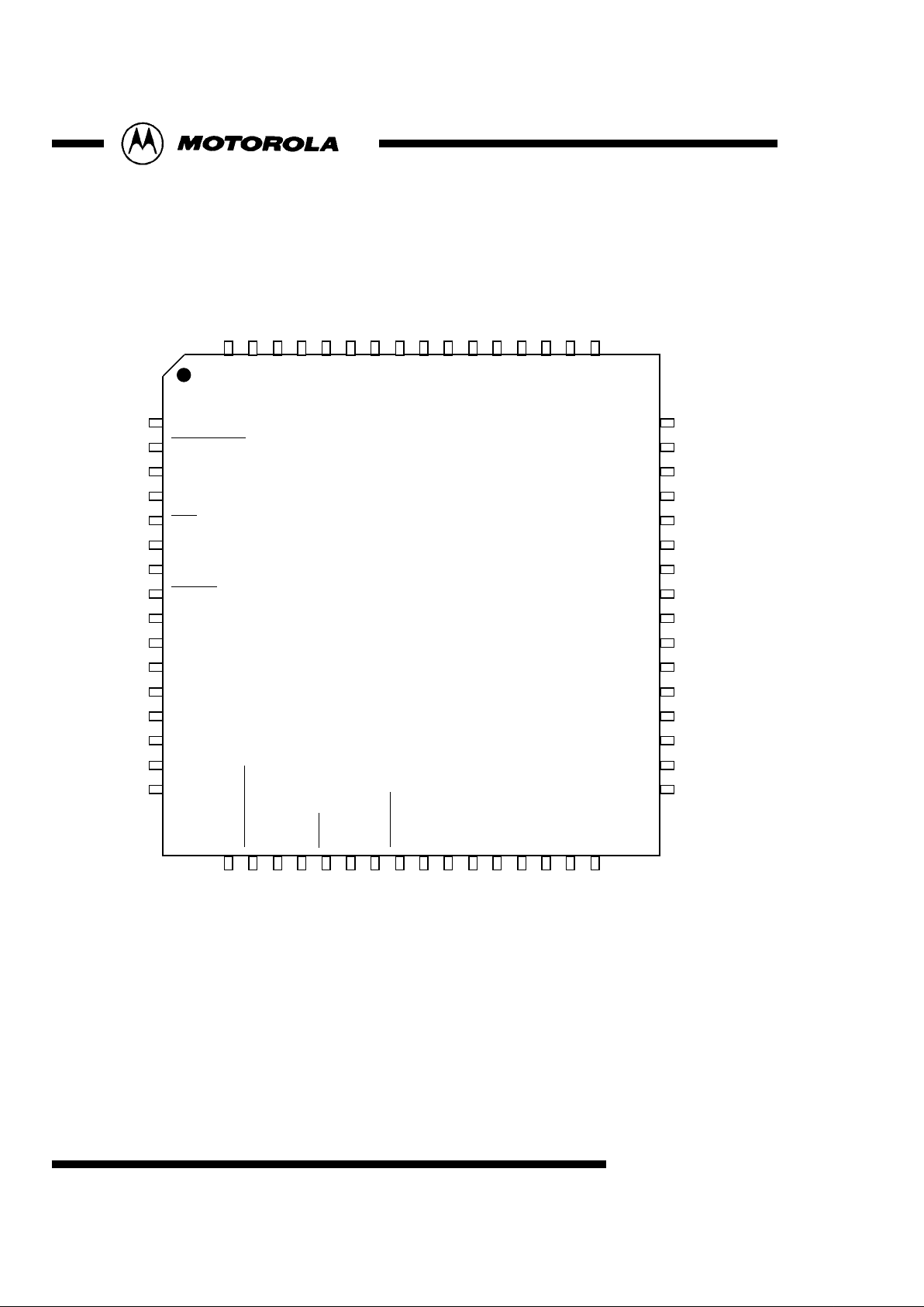
[Pin Assignment]
2
CVBS / Cb / B1
Hsync
EXT
TVIN
DVIN3
DVIN4
DVIN5
DVIN6
DVIN7
DATST
TP8
TP7
TP6
TP5
DLVss
DLVdd
TP4
MC44724
MC44725
1
2
3
4
5
6
7
8
9
12
14
15
16
17
18
19
20
21
VReff1
13
24
22
10
11
36
35
34
33
32
31
30
29
28
25
27
26
23
47
46
45
44
43
42
41
40
48
37
39
38
CVBS / Cb / B1
CVBS / Cb / B1 Vdd
Y / G1
Y / G1
Y / G1 Vdd
C / Cr / R1
C / Cr /R1
C / Cr / R1 Vdd
DAVss
Ibias1
DAVdd
ChipA
TEST
SO
SDA/SI
SCL/SCK
SEL
DVss
clock
DVdd
Reset
PAL/NTSC
DVIN0
DVIN1
DVIN2
F / Vsync
TP3
TP2
TP1
TP0
VReff2
Ibias2
NC
CVBS / Cb / B2
CVBS / Cb / B2
CVBS / Cb / B2Vdd
Y / G2
Y / G2
Y / G2 Vdd
C / Cr / R2
C / Cr / R2
C / Cr / R2 Vdd
64
63
62
61
60
57
59
49
50
51
52
53
56
54
55
58
DVss
DVdd
DVss
DVdd
MC44724/5 Rev 0.21 03/25/97
No.
This document contains information on a new product. Specifications and information herein are subject to change without notice.
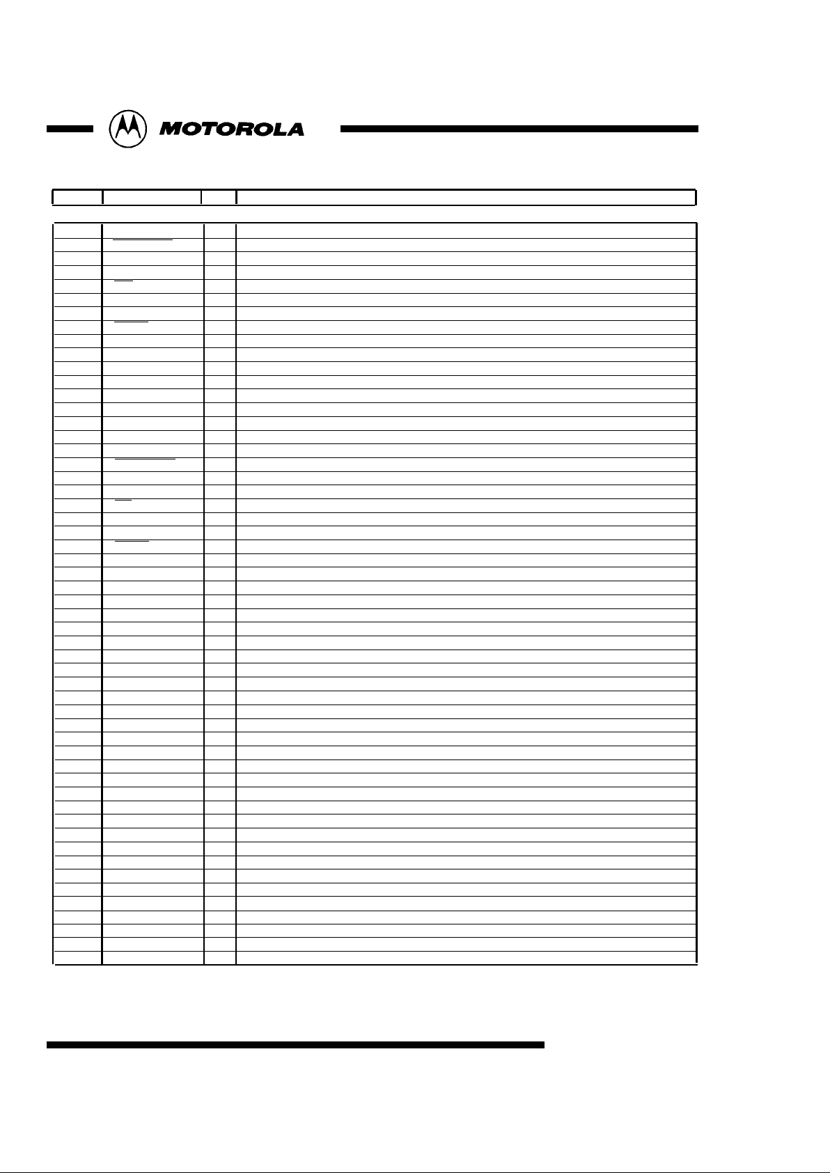
[Pin Descriptions]
1 CVBS/Cb/B1 O Analog composite video signal output or Cb or B signal output current drive(positive)
2 CVBS/Cb/B1 O Analog composite video signal output or Cb or B signal output current drive(negative)
3 CVBS/Cb/B1Vdd Power Supply for CVBS / Cb / B DAC circuit
4 Y/G1 O Analog luminance or G signal output current drive(positive)
5 Y/G1 O Analog luminance or G signal output current drive(negative)
6 Y/G1Vdd Power Supply for Y / G DAC circuit
7 C/Cr/R1 O Analog chrominance signal output or Cr or R signal output current drive(positive)
8 C/Cr/R1 O Analog chrominance signal output or Cr or R signal output current drive(negative)
9 C/Cr/R1Vdd Power Supply for C / Cr /R DAC circuit
10 DAVss Ground for DAC circuit
11 Ibias1 O Reference current for the 3 DACs1
12 Vref1 Reference full scale voltage for the 3 DACs1
13 DAVdd Power Supply for the DACs
14 Vref2 Reference full scale voltage for the 3 DACs2
15 Ibias2 O Reference current for the 3 DACs2
16 NC No Connect to pin
17 CVBS/Cb/B2 O Analog composite video signal output or Cb or B signal output current drive(positive)
18 CVBS/Cb/B2 O Analog composite video signal output or Cb or B signal output current drive(negative)
19 CVBS/Cb/B2Vdd Power Supply for CVBS / Cb / B DAC circuit
20 Y/G2 O Analog luminance or G signal output current drive(positive)
21 Y/G2 O Analog luminance or G signal output current drive(negative)
22 Y/GVdd Power Supply for Y / G DAC circuit
23 C/Cr/R2 O Analog chrominance signal output or Cr or R signal output current drive(positive)
24 C/Cr/R2 O Analog chrominance signal output or Cr or R signal output current drive(negative)
25 C/Cr/R2Vdd Power Supply for C / Cr /R DAC circuit
26 ChipA I2C chip address select { 0 : 40(hex)/41(hex) 1 : 1D(hex )/1E(hex) }
27 TEST I TEST pin(Ground)
28 DVss Ground for Digital circuit
29 CLOCK I 27MHz clock input
30 DVdd Power Supply for Digital circuit
31 Reset I Reset signal, active LOW
32 PAL/NTSC I NTSC/PAL select . This pin active only Reset time. (NTSC : Low PAL : High )
33 SO z(O) If SPI mode, serial data output / If I2C mode, connect to Ground
34 SDA/SI I/O(I) Serial data input, Open drain output / If SPI mode, serial data input
35 SCL/SCK I Serial clock
36 SEL (I) Connect to Ground / If SPI mode, this pin is chip select
37 DVdd Power Supply for Digital circuit
38 DVss Ground for Digital circuit
39~46 DVIN7~0 I/O Multiplexed 4:2:2 data(CCIR Rec656/601) input (1)
47 TVIN I/O TEST data input
48 EXT I/O Csync/Frame sync output, or external VBI information input
49 F/Vsync I/O Frame sync or Vertical sync input/output
50 Hsync I/O Horizontal sync input/output
51 DATST I MUX swith in 8-bit X 2 Multiplexed 4:2:2 data(CCIR Rec656/601) input (1) and (2), or
for D/A converter test
52~55 TP8~5 I/O 8-bit Multiplexed 4:2:2 data(CCIR Rec656/601) input (2), or Multiplexed Cr/Cb data
(CCIR Rec656/601) input in 16-bit input mode, or Test data input/output (TP8 : MSB)
56 DVss Ground for Digital circuit
57 DVdd Power Supply for Digital circuit
58~61 TP4~1 I/O Multiplexed 4:2:2 data(CCIR Rec656/601) input (2), or Multiplexed Cr/Cb data
(CCIR Rec656/601) input in 16-bit input mode, or Test data input/output (TP1 : LSB)
62 TP0 I/O Test data inout/output
63 DLVdd Power Supply D/A Converter Digital circuit
64 DLVss Ground for D/A Coverter Digital circuit
3
PIN NAME I/O DESCRIPTIONS
MC44724/5 Rev 0.21 03/25/97
No.
This document contains information on a new product. Specifications and information herein are subject to change without notice.
4
I2C/SPI chip-address 40/41(hex)
1D/1E(hex)
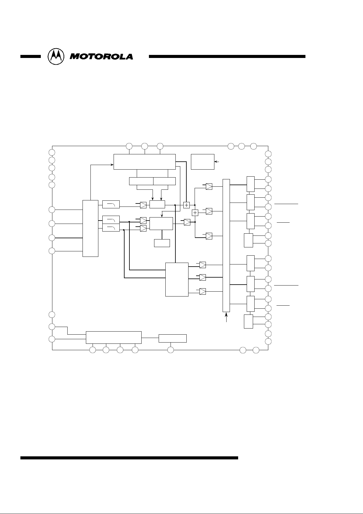
[Block Diagram]
DAC
Y/G1
Y/G1
C/Cr/R1
C/Cr/R1
CVBS/Cb/B1
CVBS/Cb/B1
Y/G1Vdd
CVBS/Cb/B1Vdd
C/Cr/R1Vdd
EXT
F/Vsync
Hsync
DVIN [7 : 0]
0
0
0
0
CGMS,
WSS_gen
CC_gen
Sync_generator
copy
protection
bus
off_set
BG
Modulator
subcarrier
gen
0
DAC
0
DAC
0
TVIN
demux
Y
Cb
Cr
H,V
ChipA
DVdd
DVdd
DVss
DVss
MC44724/5
DAVdd
DAVss
Ibias1
BIAS
Vref1
SDA/SI
SCL/SCK
TEST
TEST
PAL/NTSC
Reset
clock
SEL
SO
I2C / SPI
RGB matrix
0
0
0
DAC
Y/G2
Y/G2
C/Cr/R2
C/Cr/R2
CVBS/Cb/B2
CVBS/Cb/B2
DAC
DAC
Ibias2
BIAS
Vref2
TP [8 : 1]
DLVss
DLVdd
Y/G2Vdd
CVBS/Cb/B2Vdd
C/Cr/R2Vdd
Output Selecter
bus
TP [0]
MC44724/5 Rev 0.21 03/25/97
No.
This document contains information on a new product. Specifications and information herein are subject to change without notice.
5
Clock
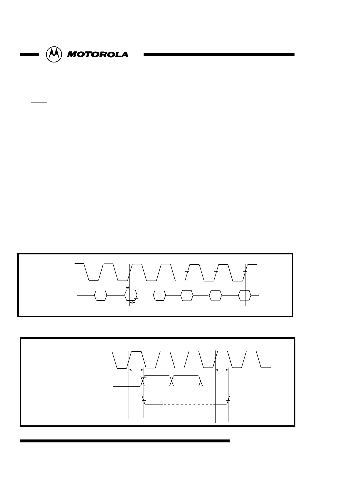
27.0Mhz is necessary. This signal on the clock pin needs to be active before the reset pin is de-asserted.
( see figures 1 and 2 )
[Function Descriptions]
Fig 1 : DVIN Data Input Timing
Input Clock 27MHz
Input Data
DVIN0~7
50%
Tds
Tdh
Clock 27MHz
Output data
H/VF sync
Output Data
TP0~8
Td
Td
Fig 2 : Sync Data Output Timing
Reset Procedure
RESET is a level sensitive input pin. Driving the RESET pin low causes a DVE reset. The 27Mhz DVE
clock signal must be active before RESET is released. De-asserting reset will latch the status of the PAL/
NTSC, TVIN and SEL pins.
The PAL/NTSC pin determines the default values for the DVE control registers. The default register
values have been chosen so that standard PAL or NTSC video will appear at the DAC outputs immediately
when a valid input digital video data stream is present.
The value on the SEL pins determine the default serial communication mode. If Low, the DVE use I2C bus
operation. If High, the DVE use 4-wired SPI operation.
After reset, the VBI signals (Closed-Caption, CGMS and WSS ) are disabled.
(see page --- for sub-address register descriptions.)
MC44724/5 Rev 0.21 03/25/97
No.
This document contains information on a new product. Specifications and information herein are subject to change without notice.
Video Timing / Sync Generator
The DVE outputs PAL-B,D,G,H,I, PAL-N, PAL-M or NTSC-M standard video signals.
The DVE sync generator can be operated in two modes, master or slave.
In master mode, the DVE generates all the correct Horizontal and Vertical or Frame sync signals
internally, or it is output Csync signal through the EXT pin(C/Fsync).
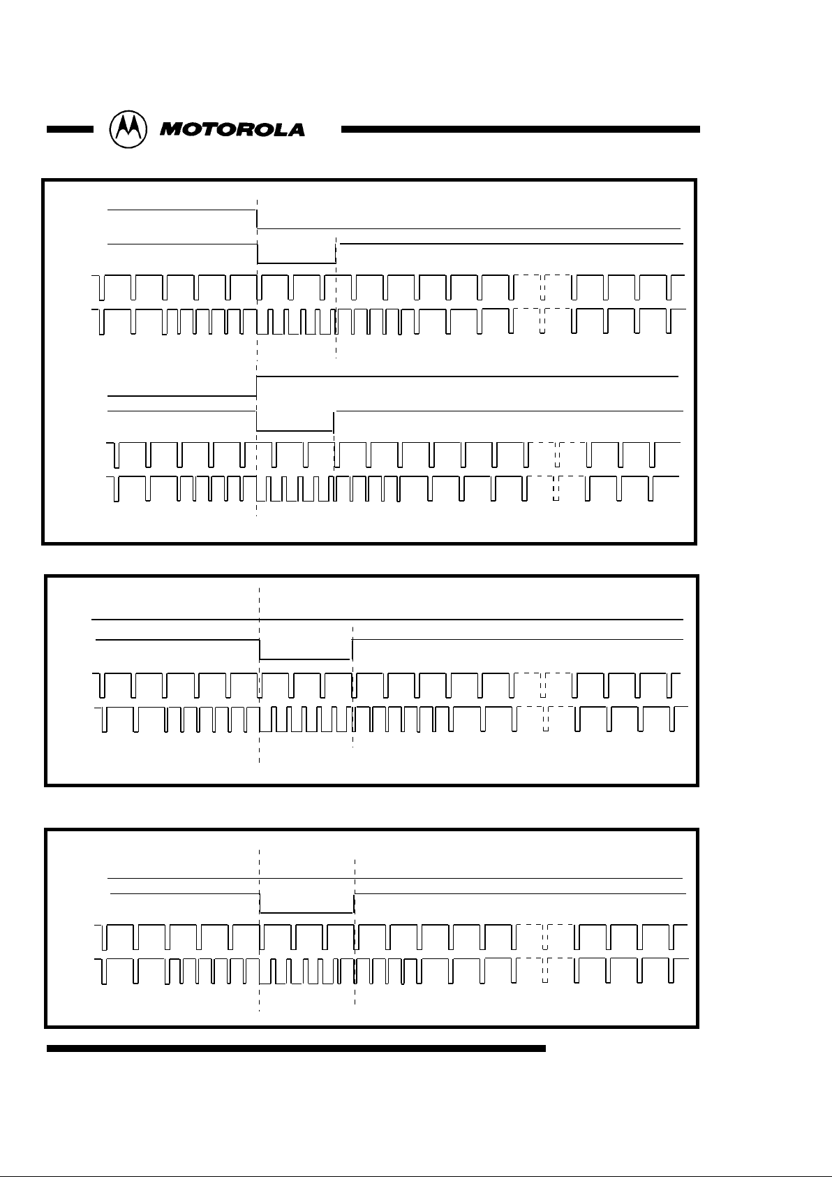
In slave mode, the DVE derives the sync signals from the Bit-Parallel input data stream Start Active
Video (SAV) and End Active Video (EAV) data packet information. Sync signals are output on the
Hsync and F/Vsync or EXT pins and can be programmed for positive or negative polarity. The phase of
Hsync can also be controlled.
Also, the DVE allows more two slave modes. One is H/Vsync slave, and the aother is H/Fsync slave
mode.
Vertical Blanking corresponds to the following lines.
625/50 624-22 311-335 ITU-R line numbering
525/60 1-19 264-282 SMPTE line numbering
(see figures 3,4,5,6,7,8,9,10, and 11 for sub-address register descriptions.)
Input Data Format
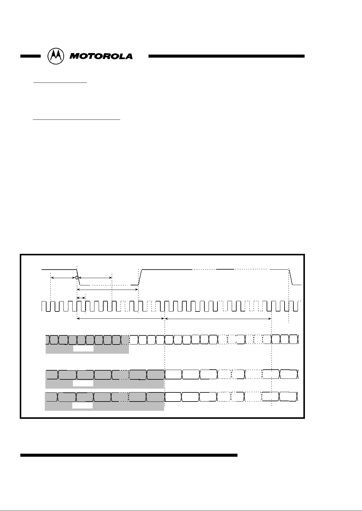
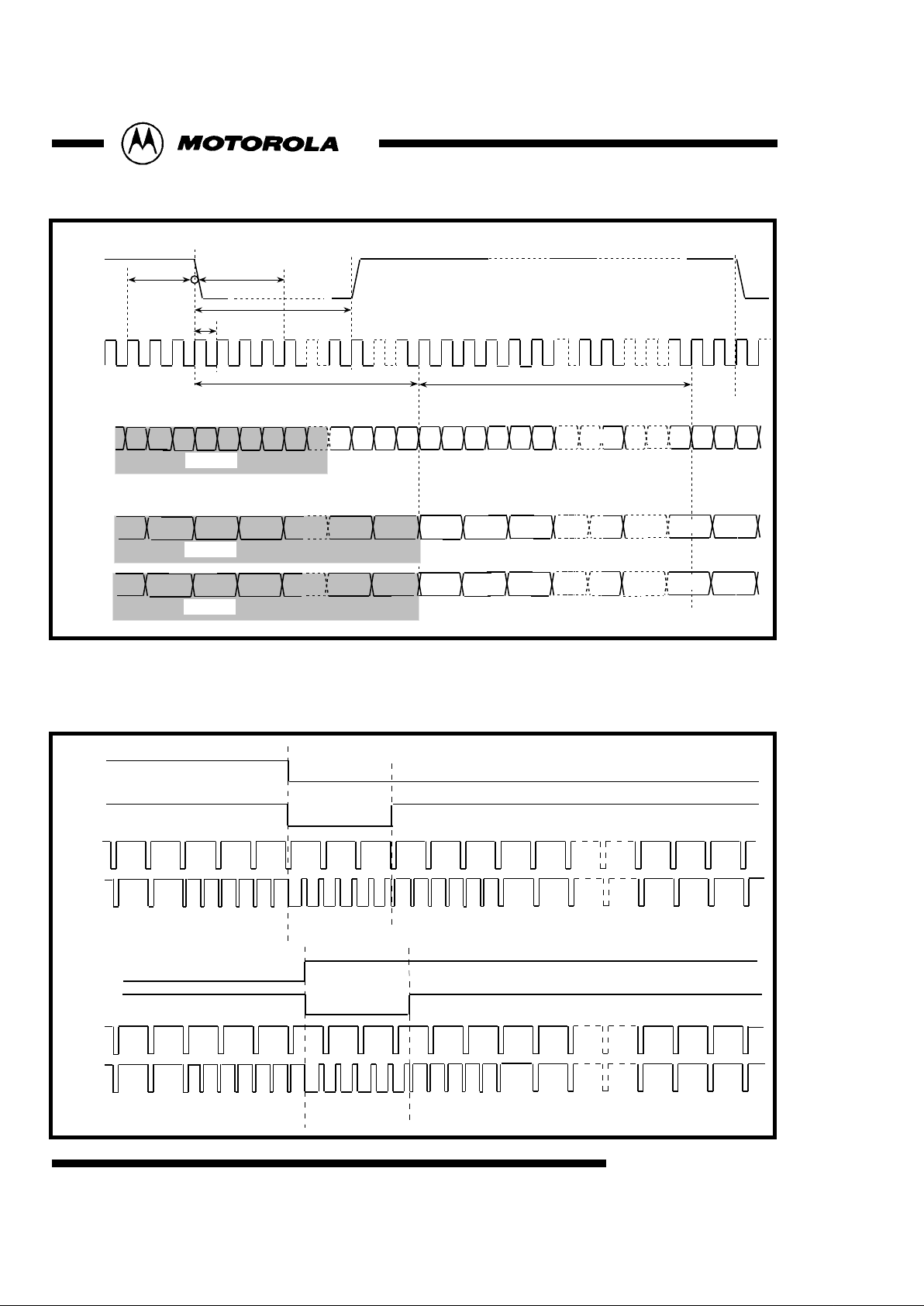
The input digital video is in accord with the ITU-R Rec.656 and SMPTE 125M standards. It is an two 8-bit
or 16-bit multiplexed 4:2:2 ((CB,Y,CR)Y) data stream. Samples are latched on the rising edge of the clock
signal. Data is input on pins DVIN[ 7 : 0 ] and TP[ 8 : 1 ]
(see figures 3 and 4 for sub-address register descriptions.)
6
Fig 3 : Digital Input Timing(525/60 system) in Master Mode
70(hex){[1:0]=01}
1440T
Hsync phase
sub-address71[2:0]
Hsync
clock
128T
T
244T
Hsync polarity
sub-address71[5]
+4T delay-3T delay
DVIN0~7
Cr718
Cb718
Y718
Y719
00 00
FF
Cb2Cr0
Cb0
Y0 Y1 Y2
INVALID
00 00 XY
FF
Y718 Y719
TP1~8
Cr718Cb718
Cb2
Cr0Cb0
INVALID
DVIN0~7
Y2
Y1Y0
INVALID
16-bit input mode
8-bit input mode
Cb718Cr718
Cr2
Cr0 Cb0
or
MC44724/5 Rev 0.21 03/25/97
No.
This document contains information on a new product. Specifications and information herein are subject to change without notice.
7
CSYNC
CSYNC
525524 1 2 3 4 5 6 7 8 9 10 11 21 22 23
262261 263 264 265 266 267 268 269 270 271 272 273 283 284 285
Fig 5 : Sync Timing::525/60 Interlaced System in Master Mode
Vsync
Hsync
Vsync
Hsync
sub-address71[7] =0
Fsync
Fsync polarity
sub-address71[3]
Vsync polarity
sub-address71[4]
Fsync
Fig 4 : Digital Input Timing(625/50 system) in Master Mode
70(hex){[1:0]=01}
1440T
Hsync phase
sub-address71[2:0]
Hsync
clock
128T
T
264T
Hsync polarity
sub-address71[5]
+4T delay-3T delay
DVIN0~7
Cr718
Cb718
Y718
Y719
00 00
FF
Cb2Cr0
Cb0
Y0 Y1 Y2
INVALID
00 00 XY
FF
Y718 Y719
TP1~8
Cr718Cb718
Cb2
Cr0Cb0
INVALID
DVIN0~7
Y2
Y1Y0
INVALID
16-bit input mode
8-bit input mode
Cb718Cr718
Cr2
Cr0 Cb0
or
MC44724/5 Rev 0.21 03/25/97
No.
This document contains information on a new product. Specifications and information herein are subject to change without notice.
8
CSYNC
262261 1 2 3 4 5 6 7 8 9 10 11 21 22 23
Fig 7 : Sync Timing::525/60 Non-interlaced System in Master Mode
CSYNC
310 311 312 1 2 3 4 6 7 8
21 22 23
5309308
Vsync
Hsync
Vsync
Hsync
Fig 8 : Sync Timing::625/50 Non-interlaced System in Master Mode
9
sub-address71[7] =1
Fsync polarity
sub-address71[3]
Vsync polarity
sub-address71[4]
Fsync
Fsync polarity
sub-address71[3]
Vsync polarity
sub-address71[4]
Fsync
sub-address71[7] =1
CSYNC
623 624 625 1 2 3 4 6 7 8
21 22 23
CSYNC
311 312 313 314 315 316 317 318 319 320 321
334 335
5622621
310309
Vsync
Hsync
Vsync
Hsync
Fig 6 : Sync Timing::625/50 Interlaced System in Master Mode
9
Fsync
Fsync polarity
sub-address71[3]
Vsync polarity
sub-address71[4]
Fsync
sub-address71[7] =0
MC44724/5 Rev 0.21 03/25/97
No.
This document contains information on a new product. Specifications and information herein are subject to change without notice.
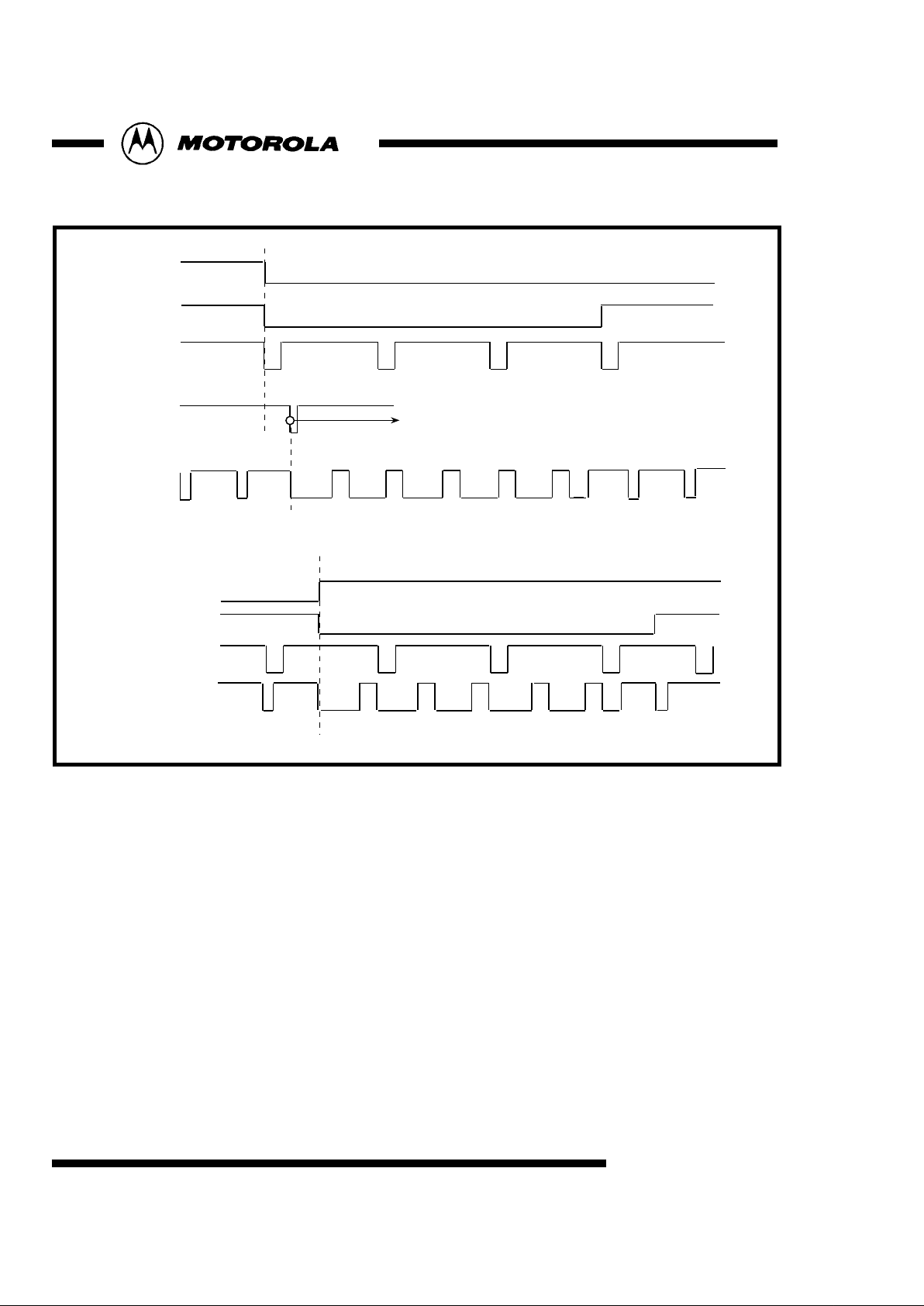
Fig 10 : Sync Timing::525/60 Interlaced System in Slave Mode
Vsync
Hsync
Fsync
Vsync polarity
sub-address71[5]
CSYNC
3 4 5 6 7
Fsync polarity
sub-address71[4]
Odd field
CSYNC
Vsync
Hsync
Fsync
266 267 268 269
Even field
sub-address71[1:0] =10, 11
Hsync Delay
sub-address 7A[7:0], 71[3:0]
Internal Hsync
reset counter
9
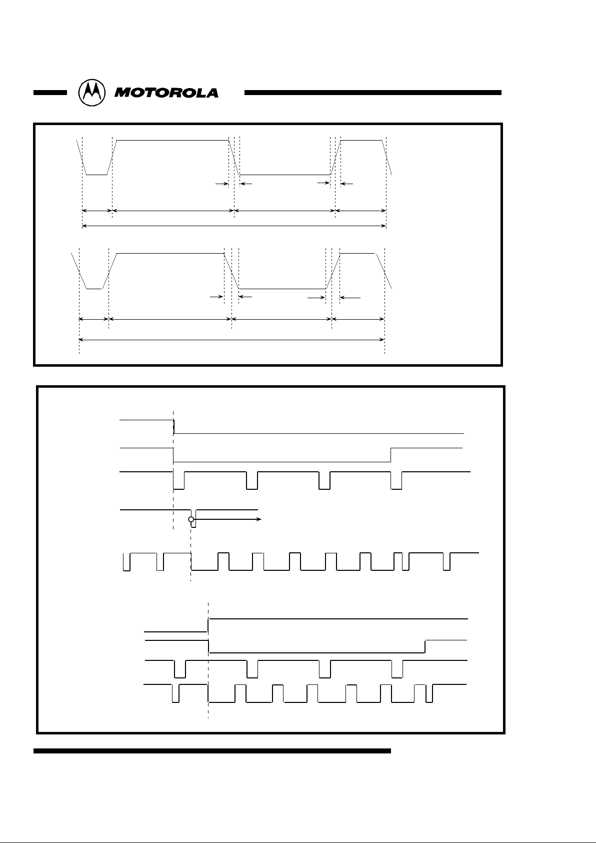
Fig 9 : Analog Sync Timing::Rise and fall
2.37uS 29.41uS 27.04uS
4.74uS
0.148uS 0.148uS
63.56uS
NTSC
PAL
0.222uS
0.222uS
2.37uS
29.63uS 27.26uS
4.74uS
64.00uS
MC44724/5 Rev 0.21 03/25/97
No.
This document contains information on a new product. Specifications and information herein are subject to change without notice.
10
Fig 11 : Sync Timing::625/50 Interlaced System in Slave Mode
Vsync
Hsync
Fsync
Vsync polarity
sub-address71[5]
Fsync polarity
sub-address71[4]
Odd field
CSYNC
625 1 2 3 4
CSYNC
Vsync
Hsync
Fsync
313 314 315 316
Even field
sub-address71[1:0] =10, 11
Hsync Delay
sub-address 7A[7:0], 71[3:0]
Internal Hsync
reset counter

MC44724/5 Rev 0.21 03/25/97
No.
This document contains information on a new product. Specifications and information herein are subject to change without notice.
Chroma / Luma Encoding
The DVE de-multiplexes the 4:2:2 digital video data stream.
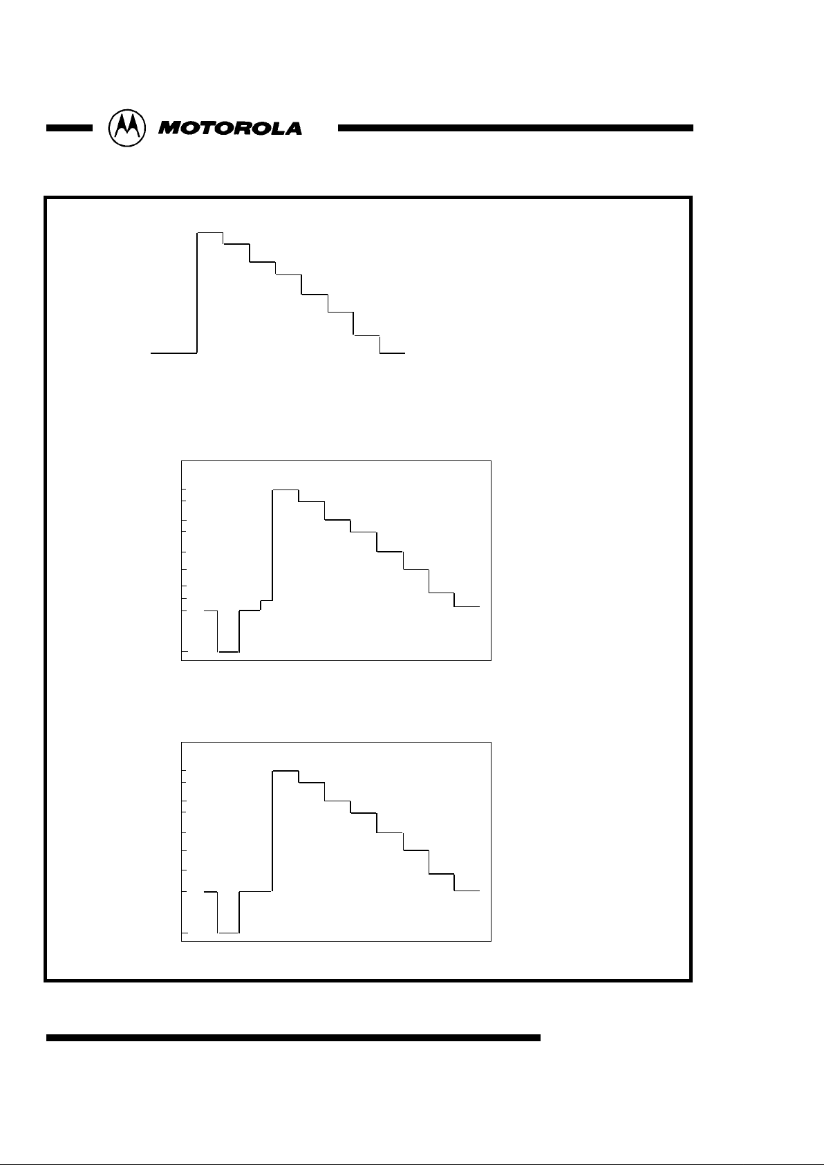
The de-multiplexed Y or Luma samples are interpolated (2X oversampled) at the clock rate. Offset
compensation is then added, next any VBI signals consisting of Closed-Caption, CGMS and WSS are
added to the appropriate lines, then finally composite sync pulses are added to the Luma signal.
(see figure 12.)
De-multiplexed component color CB and CR samples are interpolated (4X oversampled) at the clock rate.
Interpolating simplifies the output filter and allows more accurate encoding. The DVE generates the
necessary subcarrier color frequency for PAL or NTSC encoding from the 27Mhz system clock. This
color subcarrier is then modulated by the base band component color CB and CR signals to create the
video Chroma signal. (see figure 13.)
A 7.5 IRE pedestal is added for the 60Hz field rate. This can be added for the 50Hz field rate through
serial bus control. (see sub-address register descriptions)
11
CVBS and S-VIDEO or YCbCr or RGB Outputs
The internal digital video signals drive 10-bit D/A converters. Converter outputs are bi-directional current
sources where the current is proportional to the digital data with reference to the IBIAS reference current. The
pins CVBS/Cb/B, Y/G and C/Cr/R are the respective composite, Luma and Chroma or Y/Cb/Cr or R/G/B signal
current source pins. Also, each DACs can drive 75ohm load register.
User can select 2 sets of signals within above 3 sets.
(see "Application Diagram" and "sub-address register descriptions".)
Bias Current Gain
DACs can be switched off through serial bus control to reduce power consumption. Both outputs of unused
DACs should be connected to ground through a resister to avoid charge buildup.
MC44724/5 Rev 0.21 03/25/97
No.
This document contains information on a new product. Specifications and information herein are subject to change without notice.
Fig 12 : Luminance Output Range
12
212
32
470
420
340
290
162
82
32
Digital Y input code(16~235)
525/60 and 625/50 system
100%amplitude,100%saturation color bar
0
7.5
30
41
59
70
89
100
-40
IRE
670
620
540
490
412
362
282
232
12
232
Analog Y output level(525/60 system)
100%amplitude,100%saturation color bar
0
code
1023
200
0
11
30
41
59
70
89
100
-43
IRE
670
620
540
490
412
362
282
232
44
232
Analog Y output level(625/50 system)
100%amplitude,100%saturation color bar
0
code
1023
11
 Loading...