

MOTOROLA MC44608P40, MC44608P75 Datasheet
MC44608
Few External Components
Reliable and Flexible
GreenLine
V ery High V oltage
PWM Controller
The MC44608 is a high performance voltage mode controller
designed for off–line converters. This high voltage circuit that
integrates the start–up current source and the oscillator capacitor,
requires few external components while offering a high flexibility and
reliability .
The device also features a very high efficiency stand–by
management consisting of an effective Pulsed Mode operation. This
technique enables the reduction of the stand–by power consumption to
approximately 1W while delivering 300mW in a 150W SMPS.
• Integrated Start–Up Current Source
• Lossless Off–Line Start–Up
• Direct Off–Line Operation
• Fast Start–Up
General Features
• Flexibility
• Duty Cycle Control
• Undervoltage Lockout with Hysteresis
• On Chip Oscillator Switching Frequency 40, or 75kHz
• Secondary Control with Few External Components
Protections
• Maximum Duty Cycle Limitation
• Cycle by Cycle Current Limitation
• Demagnetization (Zero Current Detection) Protection
• “Over V
•
Programmable Low Inertia Over Voltage Protection Against Open Loop
• Internal Thermal Protection
GreenLine Controller
• Pulsed Mode T echniques for a Very High Efficiency Low Power
Mode
• Lossless Startup
• Low dV/dT for Low EMI Radiations
Protection” Against Open Loop
CC
http://onsemi.com
8
DIP–8
P SUFFIX
CASE 626
PIN CONNECTIONS AND
MARKING DIAGRAM
1 8
Demag
2
I
sense
Control Input
Device
MC44608P40 40kHz
MC44608P75 75kHz
3
4
Gnd
AWL = Manufacturing Code
YYWW = Date Code
(Top View)
ORDERING INFORMATION
Switching
Frequency
1
AWL
YYWW
44608Pxxx
Package
7
6
5
Plastic
DIP–8
Plastic
DIP–8
Vi
V
cc
Driver
Shipping
50 / Rail
50 / Rail
Semiconductor Components Industries, LLC, 1999
January , 2000 – Rev. 2
1 Publication Order Number:
MC44608/D
Isense
10
S1
2
DMG
Demag
Logic
Output
Start–up
200 A
m
Phase
Stand–by
Leading Edge
+
–
Switching
Phase
&
Blanking
50 mV
/20 mV
Latched off
Phase
Start–up
Phase
Stand–by
Management
Output
MC44608
REPRESENTATIVE BLOCK DIAGRAM
Demag Vi
18
>24 A
m
>120 A
m
Latched off Phase
Start–up Phase
Switching Phase
2 S
m
&
OSC
1 V
Enable
OSC
NOCOC
+
CS
–
Clock
+
PWM
&
–
VPWM
4 kHz Filter
&
&
Regulation
Block
S
R
Latched off Phase
UVLO2
OVP
UVLO1
UVLO2
OUT Disable
DMG
Thermal
Shutdown
PWM
Latch
Q
Stand–by
9 mA
Switching Phase
Start–up
Source
V
CC
Management
&
S2 S3
Buffer
6
V
CC
5
Driver
4
GND
3
Control
Input
MAXIMUM RATINGS
Rating Symbol Value Unit
Total Power Supply Current I
Output Supply Voltage with Respect to Ground V
All Inputs except Vi V
Line Voltage V
Power Dissipation and Thermal Characteristics
Maximum Power Dissipation at TA = 85°C P
Thermal Resistance, Junction–to–Air R
Operating Junction Temperature T
Operating Ambient Temperature T
CC
CC
inputs
i
D
θJA
J
A
30 mA
16 V
–1.0 to +16 V
500 V
600 mW
100 °C/W
150 °C
–25 to +85 °C
http://onsemi.com
2
MC44608
ELECTRICAL CHARACTERISTICS
Characteristic Symbol Min Typ Max Unit
OUTPUT SECTION
Output Resistor
Sink Resistance R
Source Resistance R
stup–th
(1)
(1)
= –1.0 mA 4.75 5.0 5.25 V
pin3
= +500 mA
pin3
= +1.0 mA V
pin3
Output Voltage Rise Time (from 3 V up to 9 V)
Output Voltage Falling Edge Slew–Rate (from 9 V down to 3 V)
CONTROL INPUT SECTION
Duty Cycle @ I
Duty Cycle @ I
Control Input Clamp Voltage (Switching Phase) @ I
Latched Phase Control Input Voltage (Stand–by) @ I
Latched Phase Control Input Voltage (Stand–by) @ I
CURRENT SENSE SECTION
Maximum Current Sense Input Threshold V
Input Bias Current I
Stand–By Current Sense Input Current I
Start–up Phase Current Sense Input Current I
Propagation Delay (Current Sense Input to Output @ VTH T MOS = 3 V) T
Leading Edge Blanking Duration MC44608P40 T
Leading Edge Blanking Duration MC44608P75 T
Leading Edge Blanking Duration MC44608P100 T
Leading Edge Blanking + Propagation Delay MC44608P40 T
Leading Edge Blanking + Propagation Delay MC44608P75 T
Leading Edge Blanking + Propagation Delay MC44608P100 T
OSCILLATOR SECTION
Normal Operation Frequency MC44608P40 f
Normal Operation Frequency MC44608P75 f
Normal Operation Frequency MC44608P100 f
Maximum Duty Cycle @ f = f
OVERVOLTAGE SECTION
Quick OVP Input Filtering (R
Propagation Delay (I
Quick OVP Current Threshold I
Protection Threshold Level on V
Minimum Gap Between V
NOTES:
(1) This parameter is measured using 1.0 nF connected between the output and the ground.
= 2.5 mA d
pin3
= 1.0 mA d
pin3
osc
= 100 kW)
demag
> I
demag
CC–OVP
to output low) T
ovp
CC
and V
OL
OH
t
r
t
f
2mA
1mA
V
LP–stby
LP–stby
CS–th
B–cs
CS–stby
CS–stup
PLH(In/Out)
LEB
LEB
LEB
DLY
DLY
DLY
osc
osc
osc
d
max
T
filt
PHL(In/Out)
OVP
V
CC–OVP
V
CC–OVP
V
stup
5.0 8.5 15
15
50 ns
50 ns
36 43 48 %
3.4 3.9 4.3 V
2.4 3.0 3.7 V
0.95 1.0 1.05 V
–1.8 1.8
180 200 220
180 200 220
220 ns
480 ns
250 ns
200 ns
500 680 900 ns
370 470 570 ns
400 ns
36 40 44 kHz
68 75 82 kHz
100 kHz
78 82 86 %
250 ns
2.0 µs
105 120 140 µA
14.8 15.3 15.8 V
–
1.0 V
2.0 %
m
m
m
W
A
A
A
http://onsemi.com
3
MC44608
ELECTRICAL CHARACTERISTICS (V
noted) (Note 1)
Characteristic
DEMAGNETIZATION DETECTION SECTION (Note 2)
Demag Comparator Threshold (V
Demag Comparator Hysteresis (Note 3) H
Propagation Delay (Input to Output, Low to High) t
Input Bias Current (V
Negative Clamp Level (I
Positive Clamp Level @ I
Positive Clamp Level @ I
OVERTEMPERATURE SECTION
Trip Level Over Temperature T
Hysteresis T
STAND–BY MAXIMUM CURRENT REDUCTION SECTION
Normal Mode Recovery Demag Pin Current Threshold I
K FACTORS SECTION FOR PULSED MODE OPERATION
I
/ I
CCS
stup MC44608P40
I
/ I
CCS
stup MC44608P75
I
/ I
CCS
stup MC44608P100
I
/ I
CCL
stup
(V
– UVLO2) / (V
stup
(UVLO1 – UVLO2) / (V
ICS / V
csth
Demag ratio I
(V3 1 mA – V3
V
Latch–off V3 4.8 V
control
SUPPLY SECTION
Minimum Start–up Voltage Vi
VCC Start–up Voltage V
Output Disabling VCC Voltage After Turn On V
Hysteresis (V
VCC Undervoltage Lockout Voltage V
Hysteresis (V
Absolute Normal Condition VCC Start Current @ (Vi = 100 V) and
(VCC = 9 V)
Switching Phase Supply Current (no load)
Latched Off Phase Supply Current I
Hiccup Mode Duty Cycle (no load)
NOTES:
(1) Adjust VCC above the start–up threshold before setting to 12 V . Low duty cycle pulse techniques are used during test to maintain junction
temperature as close to ambient as possible.
(2) This function can be inhibited by connecting pin 1 to GND.
(3) Guaranteed by design (non tested)
/ I
ovp
0.5 mA
stup–th
uvlo1
demag
demag
stup
stup
NM Dmgr 3.0 4.7 5.5 –
dem
) / (1 mA – 0.5 mA) R3 1800
– V
– V
uvlo2
pin1
= 50 mV) I
= –1 mA) V
= 125 mA
demag
= 25 mA
demag
– UVLO1) 102 x K
– UVLO1) 102 x K
) H
uvlo1
) H
= 12 V , for typical values TA = 25°C, for min/max values TA = –25°C to +85°C unless otherwise
CC
Symbol Min Typ Max Unit
increasing) V
PHL(In/Out)
cl–neg–dem
106 x Y
uvlo1–uvlo2
MC44608P40
MC44608P75
MC44608P100
dmg–th
dmg
dem–lb
V
cl–pos–
dem–H
V
cl–pos–
dem–L
high
hyst
dem–NM
10 x K1 2.4 2.9 3.8 –
10 x K1 2.8 3.3 4.2 –
10 x K1 3.5 –
103 x K2 46 52 63 –
sstup
sl
cstby
low
stup–th
uvlo1
stup–uvlo1
uvlo2
–(ICC) 7.0 9.5 12.8 mA
I
CCS
CC–latch
d
Hiccup
30 50 69 mV
30 mV
300 ns
–0.6
–0.9 –0.7 –0.4 V
2.05 2.3 2.8 V
1.4 1.7 1.9 V
160 °C
30 °C
20 25 30
1.8 2.2 2.6 –
90 120 150 –
175 198 225 –
12.5 13.1 13.8 V
9.5 10 10.5 V
3.1 V
6.2 6.6 7.0 V
3.4 V
2.0
2.4
–
0.3 0.5 0.68 mA
2.6
3.2
3.4
10 %
50 V
3.6
4.0
–
m
m
W
mA
A
A
http://onsemi.com
4
MC44608
PIN FUNCTION DESCRIPTION
Pin Name Description
1 Demag The Demag pin offers 3 different functions: Zero voltage crossing detection (50mV), 24µA current detection
2 I
3 Control Input A feedback current from the secondary side of the SMPS via the opto–coupler is injected into this pin. A
4 Ground This pin is the ground of the primary side of the SMPS.
5 Driver The current and slew rate capability of this pin are suited to drive Power MOSFETs.
6 V
7 This pin is to provide isolation between the Vi pin 8 and the VCC pin 6.
8 Vi This pin can be directly connected to a 500V voltage source for start–up function of the IC. During the
sense
CC
and 120µA current detection. The 24µA level is used to detect the secondary reconfiguration status and the
120µA level to detect an Over Voltage status called Quick OVP.
The Current Sense pin senses the voltage developed on the series resistor inserted in the source of the
power MOSFET. When I
Current Protection function. A 200µA current source is flowing out of the pin 3 during the start–up phase and
during the switching phase in case of the Pulsed Mode of operation. A resistor can be inserted between the
sense resistor and the pin 3, thus a programmable peak current detection can be performed during the SMPS
stand–by mode.
resistor can be connected between this pin and GND to allow the programming of the Burst duty cycle during
the Stand–by mode.
This pin is the positive supply of the IC. The driver output gets disabled when the voltage becomes higher
than 15V and the operating range is between 6.6V and 13V . An intermediate voltage level of 10V creates a
disabling condition called Latched Off phase.
Start–up phase a 9 mA current source is internally delivered to the VCC pin 6 allowing a rapid charge of the
VCC capacitor. As soon as the IC starts–up, this current source is disabled.
reaches 1V, the Driver output (pin 5) is disabled. This is known as the Over
sense
OPERATING DESCRIPTION
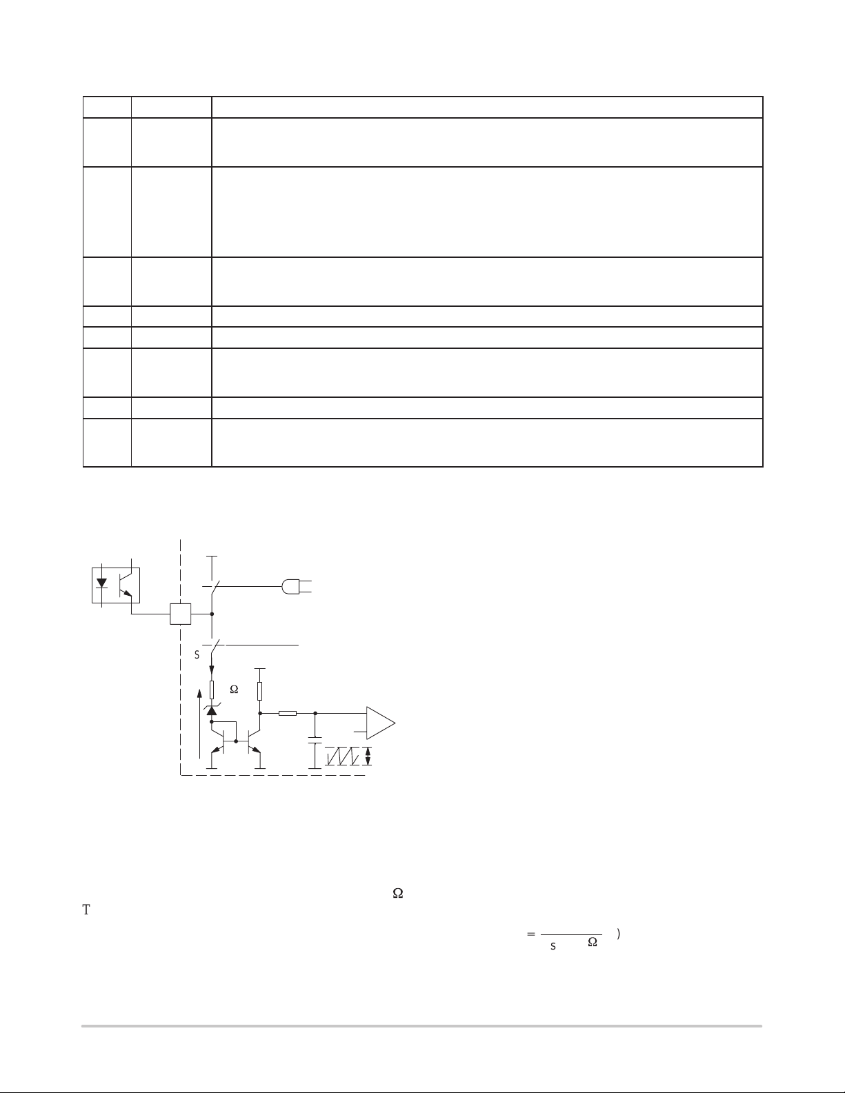
Regulation
V
V
CC
Control
Input
LP–stby
10
S3
Stand–by
&
Latched off Phase
3
5 V
10
S2
V
dd
20
W
4 kHz
Filter
Regulation
Output
Switching Phase
Comparator
PWM
1.6 V
Figure 1. Regulator
The pin 3 senses the feedback current provided by the opto
coupler. During the switching phase the switch S2 is closed
and the shunt regulator is accessible by the pin 3. The shunt
regulator voltage is typically 5V. The dynamic resistance of
the shunt regulator represented by the zener diode is 20W.
The gain of the Control input is given on Figure 10 which
shows the duty cycle as a function of the current injected into
the pin 3.
A 4kHz filter network is inserted between the shunt
regulator and the PWM comparator to cancel the high
frequency residual noise.
The switch S3 is closed in Stand–by mode during the
Latched Off Phase while the switch S2 remains open. (See
section PULSED MODE DUTY CYCLE CONTROL).
The resistor Rdpulsed (Rduty cycle burst) has no effect on
the regulation process. This resistor is used to determine the
burst duty cycle described in the chapter “Pulsed Duty Cycle
Control” on page 8.
PWM Latch
The MC44608 works in voltage mode. The on–time is
controlled by the PWM comparator that compares the
oscillator sawtooth with the regulation block output (refer to
the block diagram on page 2).
The PWM latch is initialized by the oscillator and is reset
by the PWM comparator or by the current sense comparator
in case of an over current. This configuration ensures that
only a single pulse appears at the circuit output during an
oscillator cycle.
Current Sense
The inductor current is converted to a positive voltage by
inserting a ground reference sense resistor R
Sense
in series
with the power switch.
The maximum current sense threshold is fixed at 1V. The
peak current is given by the following equation:
Ipk
max
+
R
sense
1
(A)
(W)
http://onsemi.com
5
 Loading...