

1
Device
Operating
Temperature Range
Package
MIXED FREQUENCY MODE
GREENLINE PWM*
CONTROLLER:
ORDERING INFORMATION
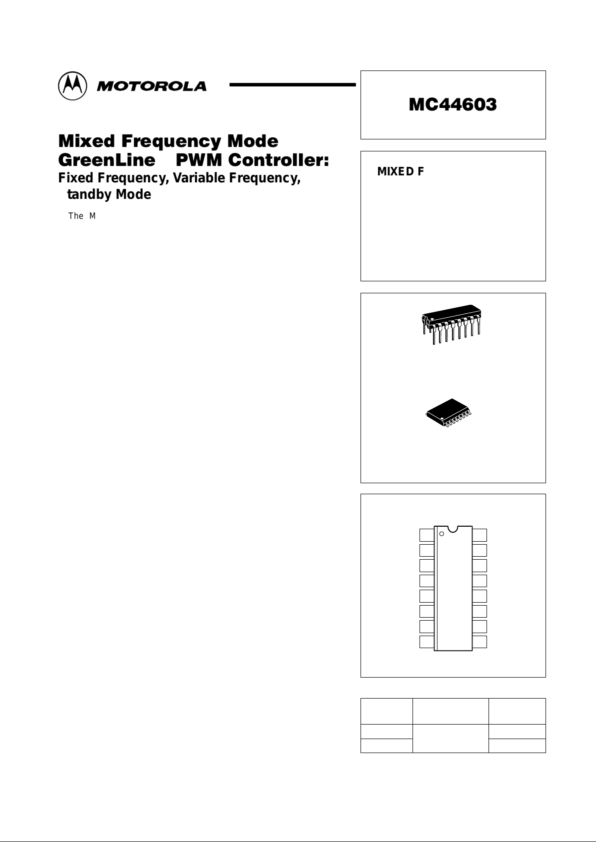
MC44603P
TA = –25° to +85°C
Plastic DIP–16
P SUFFIX
PLASTIC PACKAGE
CASE 648
16
1
16
15
14
13
12
11
10
9
2
3
4
5
6
7
8
(Top View)
V
CC
V
C
Output
R
ref
Sync Input
PIN CONNECTIONS
Order this document by MC44603/D
Gnd
Foldback Input
Overvoltage
Protection (OVP)
Current Sense Input
Demag Detection
R
Frequency
Standby
Voltage Feedback
Input
Error Amp Output
R
Power Standby
Soft–Start/D
max
/
Voltage Mode
C
T
V ARIABLE FREQUENCY,
FIXED FREQUENCY,
ST ANDBY MODE
* PWM = Pulse Width Modulation
MC44603DW SOP–16L
16
1
DW SUFFIX
PLASTIC PACKAGE
CASE 751G
(SOP–16L)
1
MOTOROLA ANALOG IC DEVICE DATA
Fixed Frequency, Variable Frequency,
Standby Mode
The MC44603 is an enhanced high performance controller that is
specifically designed for off–line and dc–to–dc converter applications. This
device has the unique ability of automatically changing operating modes if
the converter output is overloaded, unloaded, or shorted, offering the
designer additional protection for increased system reliability. The MC44603
has several distinguishing features when compared to conventional SMPS
controllers. These features consist of a foldback facility for overload
protection, a standby mode when the converter output is slightly loaded, a
demagnetization detection for reduced switching stresses on transistor and
diodes, and a high current totem pole output ideally suited for driving a power
MOSFET. It can also be used for driving a bipolar transistor in low power
converters (< 150 W). It is optimized to operate in discontinuous mode but
can also operate in continuous mode. Its advanced design allows use in
current mode or voltage mode control applications.
Current or Voltage Mode Controller
• Operation up to 250 kHz Output Switching Frequency
• Inherent Feed Forward Compensation
• Latching PWM for Cycle–by–Cycle Current Limiting
• Oscillator with Precise Frequency Control
High Flexibility
• Externally Programmable Reference Current
• Secondary or Primary Sensing
• Synchronization Facility
• High Current Totem Pole Output
• Undervoltage Lockout with Hysteresis
Safety/Protection Features
• Overvoltage Protection Against Open Current and Open Voltage Loop
• Protection Against Short Circuit on Oscillator Pin
• Fully Programmable Foldback
• Soft–Start Feature
• Accurate Maximum Duty Cycle Setting
• Demagnetization (Zero Current Detection) Protection
• Internally Trimmed Reference
GreenLine Controller: Low Power Consumption in Standby Mode
• Low Startup and Operating Current
• Fully Programmable Standby Mode
• Controlled Frequency Reduction in Standby Mode
• Low dV/dT for Low EMI Radiations
GreenLine is a trademark of Motorola, Inc.
Motorola, Inc. 1999 Rev 1
MC44603
2
MOTOROLA ANALOG IC DEVICE DATA
MAXIMUM RATINGS
Rating Symbol Value Unit
Total Power Supply and Zener Current (ICC + IZ) 30 mA
Supply Voltage with Respect to Ground (Pin 4) V
C
V
CC
18 V
Output Current (Note 1) mA
Source I
O(Source)
–750
Sink I
O(Sink)
750
Output Energy (Capacitive Load per Cycle) W 5.0 µJ
RF
Stby
, CT, Soft–Start, R
ref
, RP
Stby
Inputs V
in
–0.3 to 5.5 V
Foldback Input, Current Sense Input,
E/A Output, Voltage Feedback Input,
Overvoltage Protection, Synchronization Input
V
in
–0.3 to
VCC + 0.3
V
Synchronization Input
High State Voltage V
IH
VCC + 0.3 V
Low State Reverse Current V
IL
–20 mA
Demagnetization Detection Input Current mA
Source I
demag–ib (Source)
–4.0
Sink I
demag–ib (Sink)
10
Error Amplifier Output Sink Current I
E/A (Sink)
20 mA
Power Dissipation and Thermal Characteristics
P Suffix, Dual–In–Line, Case 648
Maximum Power Dissipation at TA = 85°C P
D
0.6 W
Thermal Resistance, Junction–to–Air R
θJA
100 °C/W
DW Suffix, Surface Mount, Case 751G
Maximum Power Dissipation at TA = 85°C P
D
0.45 W
Thermal Resistance, Junction–to–Air R
θJA
145 °C/W
Operating Junction Temperature T
J
150 °C
Operating Ambient Temperature T
A
–25 to +85 °C
NOTES: 1. Maximum package power dissipation limits must be observed.
2. ESD data available upon request.
ELECTRICAL CHARACTERISTICS (V
CC
and VC = 12 V, [Note 3], R
ref
= 10 kΩ, CT = 820 pF, for typical values TA = 25°C,
for min/max values TA = –25° to +85°C [Note 4], unless otherwise noted.)
Characteristic
Symbol Min Typ Max Unit
OUTPUT SECTION
Output Voltage (Note 5) V
Low State (I
Sink
= 100 mA)
Low State (I
Sink
= 500 mA)
V
OL
–
–
1.0
1.4
1.2
2.0
High State (I
Source
= 200 mA)
High State (I
Source
= 500 mA)
V
OH
–
–
1.5
2.0
2.0
2.7
Output Voltage During Initialization Phase V
OL
V
pgg
VCC = 0 to 1.0 V, I
Sink
= 10 µA
OL
– –
1.0
VCC = 1.0 to 5.0 V , I
Sink
= 100 µA
–
–
0.1
1.0
V
CC
= 5.0 to 13 V,
I
Sink
= 1.0
mA
–
0.1
1.0
Output Voltage Rising Edge Slew–Rate (CL = 1.0 nF, TJ = 25°C) dVo/dT – 300 – V/µs
Output Voltage Falling Edge Slew–Rate (CL = 1.0 nF, TJ = 25°C) dVo/dT – –300 – V/µs
ERROR AMPLIFIER SECTION
Voltage Feedback Input (V
E/A out
= 2.5 V) V
FB
2.42 2.5 2.58 V
Input Bias Current (VFB = 2.5 V) I
FB–ib
–2.0 –0.6 – µA
Open Loop Voltage Gain (V
E/A out
= 2.0 to 4.0 V) A
VOL
65 70 – dB
NOTES: 3. Adjust VCC above the startup threshold before setting to 12 V.
4.Low duty cycle pulse techniques are used during test to maintain junction temperature as close to ambient as possible.
5.VC must be greater than 5.0 V.
MC44603
3
MOTOROLA ANALOG IC DEVICE DATA
ELECTRICAL CHARACTERISTICS (continued) (V
CC
and VC = 12 V , [Note 3], R
ref
= 10 kΩ, CT = 820 pF , for typical values TA = 25°C,
for min/max values TA = –25° to +85°C [Note 4], unless otherwise noted.)
Characteristic
Symbol Min Typ Max Unit
ERROR AMPLIFIER SECTION (continued)
Unity Gain Bandwidth BW MHz
TJ = 25°C – 4.0 –
TJ = –25° to +85°C – – 5.5
Voltage Feedback Input Line Regulation (VCC = 10 to 15 V) V
FBline–reg
–10 – 10 mV
Output Current mA
Sink (V
E/A out
= 1.5 V , VFB = 2.7 V)
TA = –25° to +85°C
I
Sink
2.0 12 –
Source (V
E/A out
= 5.0 V , VFB = 2.3 V)
TA = –25° to +85°C
I
Source
–2.0 – –0.2
Output Voltage Swing V
High State (I
E/A out (source)
= 0.5 mA, VFB = 2.3 V) V
OH
5.5 6.5 7.5
Low State (I
E/A out (sink)
= 0.33 mA, VFB = 2.7 V) V
OL
– 1.0 1.1
REFERENCE SECTION
Reference Output Voltage (VCC = 10 to 15 V) V
ref
2.4 2.5 2.6 V
Reference Current Range (I
ref
= V
ref/Rref
, R = 5.0 k to 25 kΩ) I
ref
–500 – –100 µA
Reference Voltage Over I
ref
Range ∆V
ref
–40 – 40 mV
OSCILLATOR AND SYNCHRONIZATION SECTION
Frequency f
OSC
kHz
TA = 0° to +70°C 44.5 48 51.5
TA = –25° to +85°C 44 – 52
Frequency Change with Voltage (VCC = 10 to 15 V) ∆f
OSC
/∆V – 0.05 – %/V
Frequency Change with Temperature (TA = –25° to +85°C) ∆f
OSC
/∆T – 0.05 – %/°C
Oscillator Voltage Swing (Peak–to–Peak) V
OSC(pp)
1.65 1.8 1.95 V
Ratio Charge Current/Reference Current I
charge/Iref
–
TA = 0° to +70°C (VCT = 2.0 V) 0.375 0.4 0.425
TA = –25° to +85°C 0.37 – 0.43
Fixed Maximum Duty Cycle = I
discharge
/(I
discharge
+ I
charge
) D 78 80 82 %
Ratio Standby Discharge Current versus IR F
Stby
(Note 6) I
disch–Stby
/ –
TA = 0° to +70°C IR F
Stby
0.46 0.53 0.6
TA = –25° to +85°C (Note 8) 0.43 – 0.63
VR F
Stby
(IR F
Stby
= 100 µA) VR F
Stby
2.4 2.5 2.6 V
Frequency in Standby Mode (RF
Stby
(Pin 15) = 25 kΩ) F
Stby
18 21 24 kHz
Current Range IR F
Stby
–200 – –50 µA
Synchronization Input Threshold Voltage (Note 7) V
inthH
V
inthL
3.2
0.45
3.7
0.7
4.3
0.9
V
Synchronization Input Current I
Sync–in
–5.0 – 0 µA
Minimum Synchronization Pulse Width (Note 8) T
Sync
– – 0.5 µs
UNDERVOLTAGE LOCKOUT SECTION
Startup Threshold V
stup–th
13.6 14.5 15.4 V
Output Disable Voltage After Threshold T urn–On (UVLO 1) V
disable1
V
TA = 0° to +70°C 8.6 9.0 9.4
TA = –25° to +85°C 8.3 – 9.6
Reference Disable Voltage After Threshold T urn–On (UVLO 2) V
disable2
7.0 7.5 8.0 V
NOTES: 13. Adjust VCC above the startup threshold before setting to 12 V.
14. Low duty cycle pulse techniques are used during test to maintain junction temperature as close to ambient as possible.
16. Standby is disabled for VR P
Stby
< 25 mV typical.
17. If not used, Synchronization input must be connected to Ground.
18. Synchronization Pulse Width must be shorter than T
OSC
= 1/f
OSC
.
MC44603
4
MOTOROLA ANALOG IC DEVICE DATA
ELECTRICAL CHARACTERISTICS (continued) (V
CC
and VC = 12 V , [Note 3], R
ref
= 10 kΩ, CT = 820 pF , for typical values TA = 25°C,
for min/max values TA = –25° to +85°C [Note 4], unless otherwise noted.)
Characteristic
Symbol Min Typ Max Unit
DEMAGNETIZATION DETECTION SECTION (Note 9)
Demagnetization Detect Input
Demagnetization Comparator Threshold (V
Pin 9
Decreasing) V
demag–th
50 65 80 mV
Propagation Delay (Input to Output, Low to High) – – 0.25 – µs
Input Bias Current (V
demag
= 65 mV) I
demag–lb
–0.5 – – µA
Negative Clamp Level (I
demag
= –2.0 mA) C
L(neg)
– –0.38 – V
Positive Clamp Level (I
demag
= 2.0 mA) C
L(pos)
– 0.72 – V
SOFT–START SECTION (Note 11)
Ratio Charge Current/I
ref
I
ss(ch)/Iref
–
TA = 0° to +70°C 0.37 0.4 0.43
TA = –25° to +85°C 0.36 – 0.44
Discharge Current (V
soft–start
= 1.0 V) I
discharge
1.5 5.0 – mA
Clamp Level V
ss(CL)
2.2 2.4 2.6 V
Duty Cycle (R
soft–start
= 12 kΩ)
Duty Cycle (V
soft–start (Pin 11)
= 0.1 V)
D
soft–start 12k
D
soft–start
36
–
42
–
49
0
%
OVERVOLTAGE SECTION
Protection Threshold Level on V
OVP
V
OVP–th
2.42 2.5 2.58 V
Propagation Delay (V
OVP
> 2.58 V to V
out
Low) 1.0 – 3.0 µs
Protection Level on V
CC
VCC
prot
V
TA = 0° to +70°C 16.1 17 17.9
TA = –25° to +85°C 15.9 – 18.1
Input Resistance – kΩ
TA = 0° to +70°C 1.5 2.0 3.0
TA = –25° to +85°C 1.4 – 3.4
FOLDBACK SECTION (Note 10)
Current Sense Voltage Threshold (V
foldback (Pin 5)
= 0.9 V) V
CS–th
0.86 0.89 0.9 V
Foldback Input Bias Current (V
foldback (Pin 5)
= 0 V) I
foldback–lb
–6.0 –2.0 – µA
STANDBY SECTION
Ratio IR P
Stby/Iref
IR P
Stby/Iref
–
TA = 0° to +70°C 0.37 0.4 0.43
TA = –25° to +85°C 0.36 – 0.44
Ratio Hysteresis (Vh Required to Return to Normal Operation from Standby
Operation)
Vh/VR P
Stby
–
TA = 0° to +70°C 1.42 1.5 1.58
TA = –25° to +85°C 1.4 – 1.6
Current Sense Voltage Threshold (VR P
Stby (Pin 12)
= 1.0 V) V
CS–Stby
0.28 0.31 0.34 V
CURRENT SENSE SECTION
Maximum Current Sense Input Threshold
(V
feedback (Pin 14)
= 2.3 V and V
foldback (Pin 6)
= 1.2 V)
V
CS–th
0.96 1.0 1.04 V
Input Bias Current I
CS–ib
–10 –2.0 – µA
Propagation Delay (Current Sense Input to Output at VTH of
MOS transistor = 3.0 V)
– – 120 200 ns
TOTAL DEVICE
Power Supply Current I
CC
mA
Startup (VCC = 13 V with VCC Increasing) – 0.3 0.45
Operating TA = –25° to +85°C (Note 3) 13 17 20
Power Supply Zener Voltage (ICC = 25 mA) V
Z
18.5 – – V
Thermal Shutdown – – 155 – °C
NOTES: 13. Adjust VCC above the startup threshold before setting to 12 V.
14. Low duty cycle pulse techniques are used during test to maintain junction temperature as close to ambient as possible.
19. This function can be inhibited by connecting Pin 8 to Gnd. This allows a continuous current mode operation.
10. This function can be inhibited by connecting Pin 5 to VCC.
11. The MC44603 can be shut down by connecting the Soft–Start pin (Pin 11) to Ground.
MC44603
5
MOTOROLA ANALOG IC DEVICE DATA
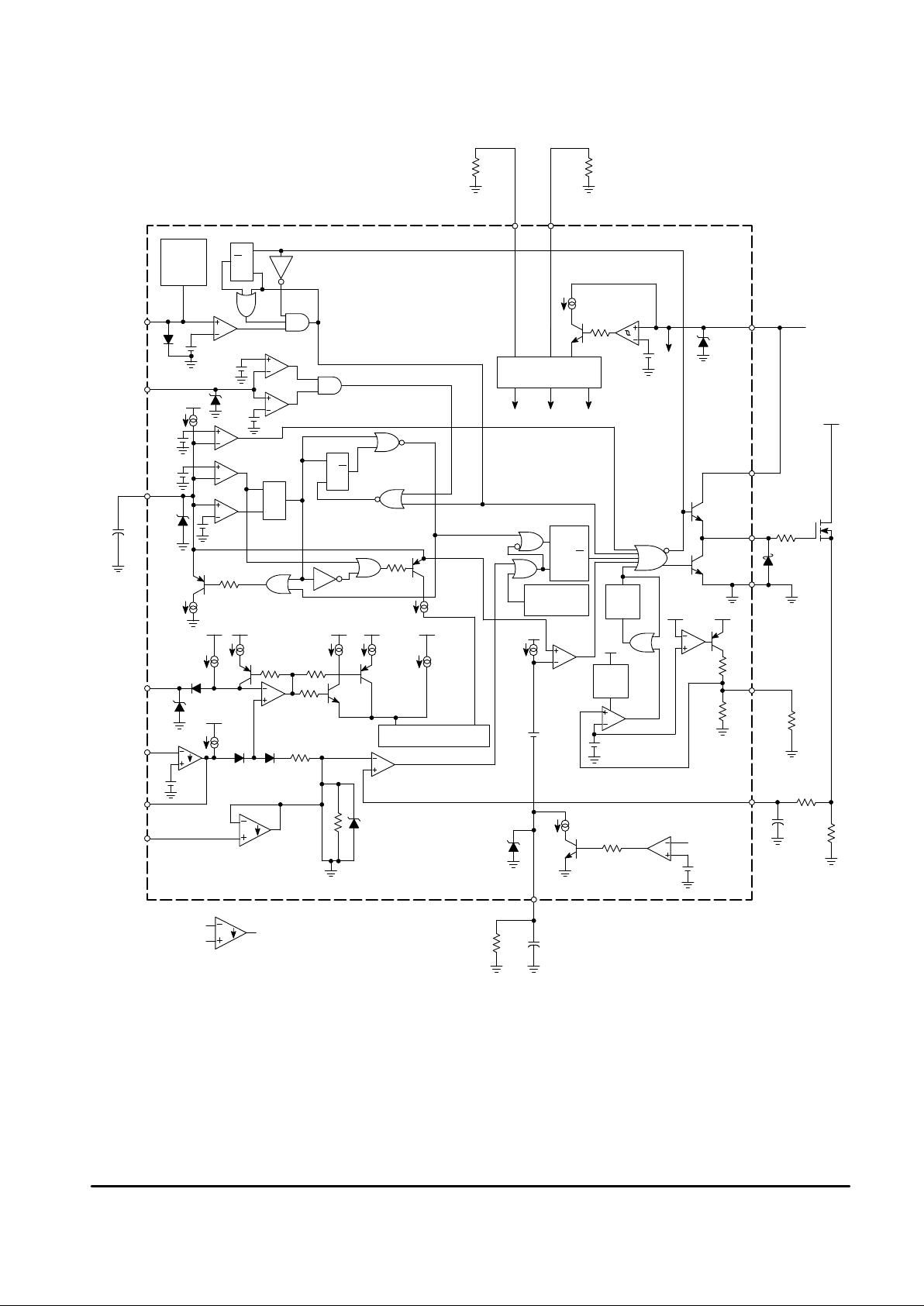
Representative Block Diagram
This device contains 243 active transistors.
S
RF
Stby
R
ref
RF
Stby
V
ref
15 16
Reference
Block
V
refIref
+
V
CC
V
CC
1
14.5 V/7.5 V
V
aux
18.0 V
To Powe
r
Transform
e
V
C
2
Output
3
Gnd
4
OVP
6
Current
Sense Input
7
V
CC
V
ref
V
OVP
Out
2.0
µ
s
Delay
V
ref
5.0
µ
s
Delay
+
2.5 V
R
OVP
11.6 k
2.0 k
V
CC
+
9.0 V
SS/D
max
/VM
2.4 V
R
SS
C
SS
11
1.0 V
Demag
Detect
8
Sync
Input
9
V
ref
+
+
+
65 mV
3.7 V
1.0 V
0.4 I
ref
C
T
10
R
Pwr Stby
12
Feed–
back
14
Compen–
sation
13
Foldback
Input
5
1.6 V
3.6 V
+
C
T
0.7 V
V
Demag Out
Synchro
V
OSC prot
0.4 I
ref
V
refVref
V
refVref
V
ref
0.4 I
ref
0.6 I
ref
0.8 I
ref
0.25
IF
Stby
0.2 I
ref
I
Discharge
I
Discharge/2
Current Mirror X2
0.4 I
ref
V
ref
2R
V
CC
1.0 mA
Error Amplifier
R
Q
S
R
Q
S
R
Q
S
R
Q
= Sink only
= Positive True Logic
+
2.5 V
Thermal
Shutdown
IF
Stby
UVLO2
V
OSC
+
1.6 V
UVLO1
5.0 mA
Negative
Active
Clamp
MC44603
6
MOTOROLA ANALOG IC DEVICE DATA
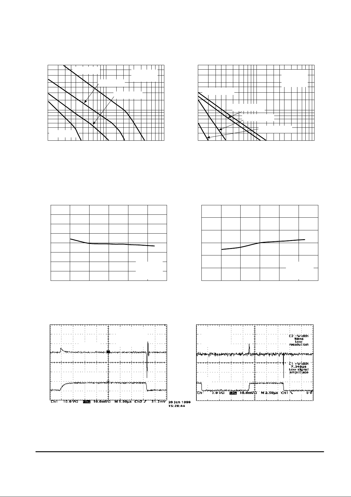
Figure 1. Timing Resistor versus
Oscillator Frequency
Figure 2. Standby Mode Timing Capacitor
versus Oscillator Frequency
10 k
10000
C
T
, TIMING CAPACIT OR (pF)
f
OSC
, Oscillator Frequency (Hz)
VCC = 16 V
TA = 25
°
C
R
ref
= 10 k
10 k
100
R
ref
, TIMING RESISTANCE (k )
Ω
f
OSC
, Oscillator Frequency (Hz)
VCC = 16 V
TA = 25
°
C
100010
3003.0
100 k100 k 1.0 Meg1.0 Meg
CT = 100 pF
CT = 500 pF
CT = 2200 pF
CT = 1000 pF
RF
Stby
= 2.0 k
RF
Stby
= 5.0 k
RF
Stby
= 27 k
RF
Stby
= 100 k
TA, AMBIENT TEMPERATURE (°C)
Figure 3. Oscillator Frequency
versus Temperature
TA, AMBIENT TEMPERATURE (°C)
Figure 4. Ratio Charge Current/Reference
Current versus Temperature
52
51
48
47
46
45
44
–50 –25 0 25 50 75 100
VCC = 12 V
R
ref
= 10 k
CT = 820 pF
0.43
0.41
0.40
0.37
0.38
–50 –25 0 25 50 75 100
0.39
f
OSC
, OSCILLATOR FREQUENCY (kHz)
= RATIO CHARGE CURRENT/I
charge
/I
ref
REFERENCE CURRENT
49
50
0.42
VCC = 12 V
R
ref
= 10 k
CT = 820 pF
Figure 5. Output Waveform Figure 6. Output Cross Conduction
V
O
I
CC
VCC = 12 V
CL = 2200 pF
TA = 25
°
C
Current
Voltage
Current
Voltage
1.0
µ
s/Div1.0 µs/Div
VCC = 12 V
CL = 2200 pF
TA = 25
°
C
600
400
–200
–400
–600
–800
–1000
I
O
, OUTPUT CURRENT (mA)
0
200
70
60
30
20
10
0
–10
V
O
, OUTPUT DRIVE VOL TAGE (V)
40
50
70
60
30
20
10
0
–10
40
50
300
200
–10
0
–20
0
–30
0
–40
0
–50
0
0
100
V
O
, OUTPUT DRIVE VOL TAGE (V)
MC44603
7
MOTOROLA ANALOG IC DEVICE DATA
500
425
400
375
350
325
300
–50 –25 0 25 50 75 100
I
source
, OUTPUT SOURCE CURRENT (mA)TA, AMBIENT TEMPERATURE (
°
C)
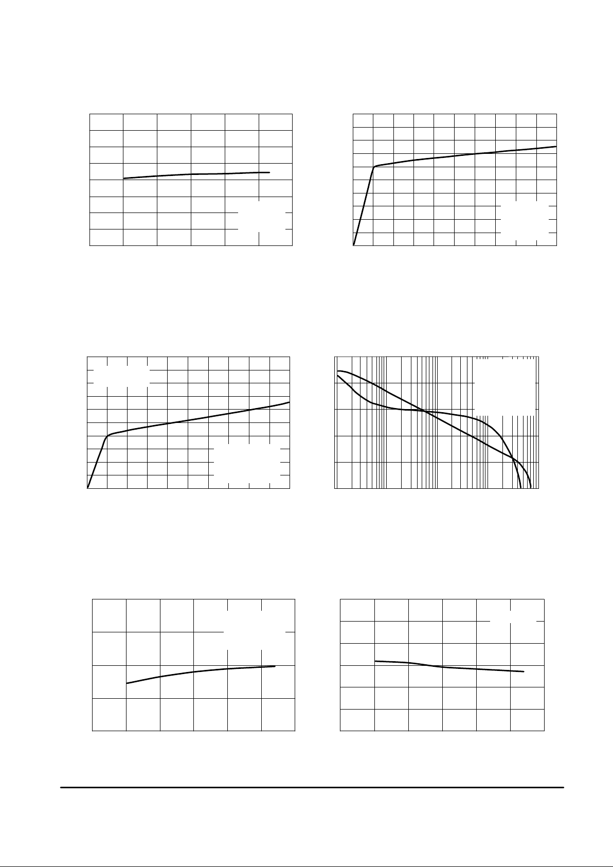
Figure 7. Oscillator Discharge Current
versus Temperature
Figure 8. Source Output Saturation Voltage
versus Load Current
2.5
2.0
1.5
1.0
0 100 200 300 400 500
I
disch
, DISCHARGE CURRENT (
µ
A)
V
OH
, SOURCE OUTPUT SATURATION VOLT AGE (V)
450
475
VCC = 12 V
R
ref
= 10 k
CT = 820 pF
VCC = 12 V
R
ref
= 10 k
CT = 820 pF
TA = 25
°
C
f, FREQUENCY (kHz)
Figure 9. Sink Output Saturation Voltage
versus Sink Current
I
sink
, SINK OUTPUT CURRENT (mA)
Figure 10. Error Amplifier Gain and Phase
versus Frequency
1.6
0
0 100
802.0
1.2
0.8
0.4
200 300 400 500
V
OL
, SINK OUTPUT SA TURATION VOLTAGE (V)
GAIN (dB)
60
40
20
0
–20
1001.0 10 1000
140
50
–40
PHASE (DEGREES)
VCC = 12 V
G = 10
Vin = 30 mV
VO = 2.0 to 4.0 V
RL = 100 k
TA = 25
°
C
TA = 25°C
VCC = 12 V
80
µ
s Pulsed Load
120 Hz Rate
Sink Saturation
(Load to VCC)
Figure 11. Voltage Feedback Input
versus Temperature
Figure 12. Demag Comparator Threshold
versus Temperature
2.60
2.55
2.40
2.45
–50 –25 0 25 50 75 100
2.50
TA, AMBIENT TEMPERATURE (
°
C)
V
FB
, VOLTAGE FEEDBACK INPUT (V)
80
75
70
65
60
50
–50 –25 0 25 50 75 100
TA, AMBIENT TEMPERATURE (
°
C)
V
demag–th
, DEMAG COMPARATOR THRESHOLD (mV)
55
VCC = 12 V
G = 10
VO = 2.0 to 4.0 V
RL = 100 k
VCC = 12 V
MC44603
8
MOTOROLA ANALOG IC DEVICE DATA
0
0
100
R
JA
, THERMAL RESISTANCE JUNCTION–TO–AIR ( C/W)
θ
80
60
40
20
10 20 30 40 50
L, LENGTH OF COPPER (mm)
°
P
D
, MAXIMUM POWER DISSIPATION (W)
5.0
4.0
3.0
2.0
1.0
0
Graphs represent symmetrical layout
3.0 mm
Printed circuit board heatsink example
L
L
2.0 oz
Copper
P
D(max)
for TA = 70°C
R
θ
JA
3.2
3.1
2.8
2.9
3.0
–50 –25 0 25 50 75 100
TA, AMBIENT TEMPERATURE (
°
C)
Figure 13. Current Sense Gain
versus Temperature
Figure 14. Thermal Resistance and Maximum
Power Dissipation versus P.C.B. Copper Length
A
VCS
, CURRENT SENSE GAIN
VCC = 12 V
R
ref
= 10 k
CT = 820 pF
VCC, SUPPLY VOLTAGE (V)
Figure 15. Propagation Delay Current Sense
Input to Output versus Temperature
TA, AMBIENT TEMPERATURE (°C)
Figure 16. Startup Current versus V
CC
PROPAGATION DELAY (ns)
STAR TUP CURRENT (mA)
0
4.00 2.0 6.0
140
120
100
80
–50 –25 0 25 50 75 100
0.35
0.30
0.25
0.20
0.15
0.10
0.05
8.0 10 12 14
VCC = 12 V
R
ref
= 10 k
CT = 820 pF
R
ref
= 10 k
CT = 820 pF
Figure 17. Supply Current versus
Supply Voltage
Figure 18. Power Supply Zener Voltage
versus Temperature
16
0
VCC, SUPPLY VOLTAGE (V)
21.0
20.5
20.0
19.5
19.0
–50 –25 0 25 50 75 100
TA, AMBIENT TEMPERATURE (
°
C)
I
CC
, SUPPLY CURRENT (mA)
V
Z
, ZENER VOLTAGE (V)
14
12
10
8.0
6.0
4.0
2.0
2.0 4.0 6.0 8.0 10 12 14 16
21.5
TA = 25°C
R
ref
= 10 k
CT = 820 pF
VFB = 0 V
VCS = 0 V
ICC = 25 mA
 Loading...