

MOTOROLA MC44602P2 Datasheet
SEMICONDUCTOR
TECHNICAL DATA
HIGH PERFORMANCE
CURRENT MODE
CONTROLLER
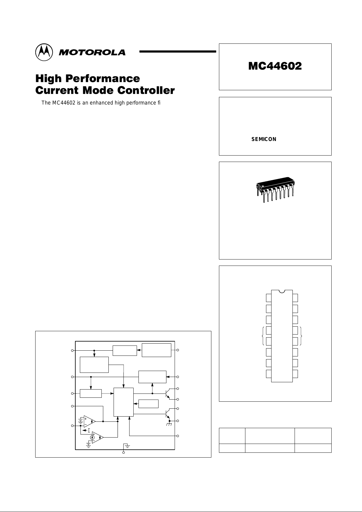
PIN CONNECTIONS
Order this document by MC44602/D
P2 SUFFIX
PLASTIC PACKAGE
CASE 648C
DIP (12 + 2 + 2)
16
1
(T op View)
Compensation
Load Detect Input
Voltage Feedback Input
Sink Gnd
Current Sense Input
Sync Input
RT/C
T
V
ref
V
CC
Sink Gnd
Source Output
Gnd
V
C
Sink Output
16
15
14
13
12
11
10
9
1
2
3
4
5
6
7
8
Device
Operating
Temperature Range
Package
ORDERING INFORMATION
MC44602 TA = –25 to 85°C DIP (12 + 2 + 2)
1
MOTOROLA ANALOG IC DEVICE DATA
The MC44602 is an enhanced high performance fixed frequency current
mode controller that is specifically designed for off–line and high voltage
dc–to–dc converter applications. This device has the unique ability of
changing operating modes if the converter output is overloaded or shorted,
offering the designer additional protection for increased system reliability.
The MC44602 has several distinguishing features when compared to
conventional current mode controllers. These features consist of a foldback
amplifier for overload detection, valid load and demag comparators with a
fault latch for short circuit detection, thermal shutdown, and separate high
current source and sink outputs that are ideally suited for driving a high
voltage bipolar power transistor, such as the MJE18002, MJE18004, or
MJE18006.
Standard features include an oscillator with a sync input, a temperature
compensated reference, high gain error amplifier, and a current sensing
comparator. Protective features consist of input and reference undervoltage
lockouts each with hysteresis, cycle–by–cycle current limiting, a latch for
single pulse metering, and a flip–flop which blanks the output off every other
oscillator cycle, allowing output deadtimes to be programmed from 50% to
70%. This device is manufactured in a 16 pin dual–in–line heat tab package
for improved thermal conduction.
• Separate High Current Source and Sink Outputs Ideally Suited for
Driving Bipolar Power Transistors: 1.0 A Source, 1.5 A Sink
• Unique Overload and Short Circuit Protection
• Thermal Protection
• Oscillator with Sync Input
• Current Mode Operation to 500 kHz Output Switching Frequency
• Output Deadtime Adjustable from 50% to 70%
• Automatic Feed Forward Compensation
• Latching PWM for Cycle–By–Cycle Current Limiting
• Input and Reference Undervoltage Lockouts with Hysteresis
• Low Startup and Operating Current
Simplified Block Diagram
Error
Amplifier
Foldback
Amplifier
16
V
ref
7
Sync Input
8
RT/C
T
1
Compensation
3
Voltage Feedback–Input
V
ref
Undervoltage
Lockout
5.0V
Reference
V
CC
Undervoltage
Lockout
Short Circuit
Detection
Oscillator
Flip Flop
and
Latching
PWM
Thermal
Gnd 9
15
V
CC
2
11
6
Load Detect Input
14
V
C
Source Output
10
Sink Output
4, 5, 12, 13
Sink Ground
Current Sense Input
Motorola, Inc. 1996 Rev 0
MC44602
2
MOTOROLA ANALOG IC DEVICE DATA
MAXIMUM RATINGS
Rating Symbol Value Unit
Total Power Supply and Zener Current (ICC + IZ) 30 mA
Sink Ground Voltage
with Respect to Gnd (Pin 9)
V
Sink(neg)
–5.0 V
Output Supply Voltage
with Respect to Sink Gnd (Pins 4, 5, 12, 13)
V
C
20 V
Output Current (Note 1)
Source
Sink
I
O(Source)
I
O(Sink)
1.0
1.5
A
Output Energy (Capacitive Load per Cycle) W 5.0 µJ
Current Sense and Voltage Feedback Inputs V
in
–0.3 to 5.5 V
Sync Input
High State Voltage
Low State Reverse Current
V
IH
I
IL
5.5
–20
V
mA
Load Detect Input Current I
in
–20 to +10 mA
Error Amplifier Output Sink Current IEA
(Sink)
10 mA
Power Dissipation and Thermal Characteristics
Maximum Power Dissipation at TA = 25°C
Thermal Resistance, Junction–to–Air
Thermal Resistance, Junction–to–Case
P
D
R
θJA
R
θJC
2.5
80
15
W
°C/W
°C/W
Operating Junction Temperature T
J
150 °C
Operating Ambient Temperature T
A
–25 to +85 °C
NOTE: 1.Maximum package power dissipation limits must be observed.
ELECTRICAL CHARACTERISTICS (V
CC
and VC = 12 V [Note 2], RT = 10k, CT = 1.0 nF, for typical values TA = 25°C, for min/max
values TA = –25°C to +85°C [Note 3] unless otherwise noted.)
Characteristic
Symbol Min Typ Max Unit
ERROR AMPLIFIER SECTION
Voltage Feedback Input (VO = 2.5V) V
FB
2.45 2.5 2.65 V
Input Bias Current (VFB = 2.5 V) I
IB
– –0.6 –2.0 µA
Open Loop Voltage Gain (VO = 2.0 V to 4.0 V) A
VOL
65 90 – dB
Unity Gain Bandwidth
TJ = 25°C
TA = –25 to +85°C
BW
1.0
0.8
1.4
–
1.8
2.0
MHz
Power Supply Rejection Ratio (VCC = 10 V to 16 V) PSRR 65 70 – dB
Output Current
Sink (VO = 1.5 V , VFB = 2.7 V)
Sink TJ = 25°C
Sink TA = –25 to +85°C
Source (VO = 5.0 V , VFB = 2.3 V)
Source TJ = 25°C
Source TA = –25 to +85°C
I
Sink
I
Source
–
1.5
–
–2.0
5.0
–
–1.1
–
–
10
–
–0.2
mA
Output Voltage Swing
High State (I
O(Source)
= 0.5 mA, VFB = 2.3 V)
Low State (I
O(Sink)
= 0.33 mA, VFB = 2.7 V)
V
OH
V
OL
6.0
–
7.0
1.0
–
1.1
V
NOTES: 2. Adjust VCC above the startup threshold before setting to 12V.
3.Low duty cycle pulse techniques are used during test to maintain junction temperature as close to ambient as possible.
MC44602
3
MOTOROLA ANALOG IC DEVICE DATA
ELECTRICAL CHARACTERISTICS (V
CC
and VC = 12 V [Note 2], RT = 10k, CT = 1.0 nF, for typical values TA = 25°C, for min/max
values TA = –25°C to +85°C [Note 3] unless otherwise noted.)
Characteristic
Symbol Min Typ Max Unit
OSCILLATOR SECTION
Frequency
TJ = 25°C
TA = –25°C to +85°C
f
OSC
168
160
180
–
192
200
kHz
Frequency Change with Voltage (VCC = 12 V to 18 V) ∆f
OSC
/∆V – 0.1 0.2 %/V
Frequency Change with Temperature ∆f
OSC
/∆T – 0.05 – %/°C
Oscillator Voltage Swing (Peak–to–Peak) V
OSC(pp)
1.3 1.6 – V
Discharge Current (V
OSC
= 3.0 V)
TJ = 25°C
TA = –25°C to +85°C
I
dischg
6.5
6.0
10
–
13.5
14
mA
Sync Input Threshold Voltage
High State
Low State
V
IH
V
IL
2.5
1.0
2.8
1.3
3.2
1.7
V
Sync Input Resistance
TJ = 25°C
TA = –25°C to +85°C
R
in
6.5
6.0
10
–
13.5
18
kΩ
REFERENCE SECTION
Reference Output Voltage (IO = 1.0 mA) V
ref
4.7 5.0 5.3 V
Line Regulation (VCC = 12 V to 18 V) Reg
line
– 1.0 10 mV
Load Regulation (IO = 1.0 mA to 20 mA) Reg
load
– 3.0 15 mV
T emperature Stability T
S
– 0.2 – mV/°C
Total Output Variation over Line, Load and Temperature V
ref
4.65 – 5.35 V
Output Noise Voltage (f = 10 Hz to 10 kHz, TJ = 25°C) V
n
– 50 – µV
Long Term Stability (TA = 125°C for 1000 Hours) S – 5.0 – mV
Output Short Circuit Current
TJ = 25°C
TA = –25°C to +85°C
I
SC
–
–70
–130
–
–
–180
mA
CURRENT SENSE SECTION
Current Sense Input Voltage Gain (Notes 4 & 5)
TJ = 25°C
TA = –25°C to +85°C
A
V
2.85
2.7
3.0
–
3.15
3.2
V/V
Maximum Current Sense Input Threshold (Note 4) V
th
0.9 1.0 1.1 V
Input Bias Current I
IB
– –4.0 –10 µA
Propagation Delay (Current Sense Input to Sink Output) t
PLH(in/out)
– 100 150 ns
UNDERVOLTAGE LOCKOUT SECTIONS
Startup Threshold (VCC Increasing) V
th
13 14.1 15 V
Minimum Operating Voltage After Turn–On (VCC Decreasing) V
CC(min)
9.0 10.2 11 V
Reference Undervoltage Threshold (V
ref
Decreasing) V
ref
(UVLO) 3.0 3.35 3.7 V
NOTES: 2.Adjust VCC above the startup threshold before setting to 12V.
3.Low duty cycle pulse techniques are used during test to maintain junction temperature as close to ambient as possible.
4.This parameter is measured at the latch trip point with IFB = –5.0
µA, refer to Figure 9.
5.Comparator gain is defined as AV =
∆V Current Sense Input
∆V Compensation
MC44602
4
MOTOROLA ANALOG IC DEVICE DATA
ELECTRICAL CHARACTERISTICS
(V
CC
and VC = 12 V [Note 2], RT = 10k, CT = 1.0 nF, for typical values TA = 25°C, for min/max
values TA = –25°C to +85°C [Note 3] unless otherwise noted.)
Characteristic
Symbol Min Typ Max Unit
OUTPUT SECTION
Output Voltage (TA = 25°C)
Low State (I
Sink
= 100 mA)
Low State (I
Sink
= 1.0A)
Low State (I
Sink
= 1.5 A)
High State (I
Source
= 50 mA)
High State (I
Source
= 0.5 A)
High State (I
Source
= 0.75 A)
V
OL
(VCC–VOH)
–
–
–
–
–
–
0.6
1.8
2.1
1.4
1.7
1.8
0.3
2.0
2.6
1.7
2.0
2.2
V
Output Voltage with UVLO Activated (VCC = 6.0 V , I
Sink
= 1.0 mA) V
OL(UVLO)
– 0.1 1.1 V
Output Voltage Rise T ime (CL = 1.0 nF, TJ = 25°C) t
r
– 50 150 ns
Output Voltage Fall T ime (CL = 1.0 nF, TJ = 25°C) t
f
– 50 150 ns
PWM SECTION
Duty Cycle
Maximum
Minimum
DC
(max)
DC
(min)
46
–
48
–
50
0
%
TOTAL DEVICE
Power Supply Current
Startup (VCC = 5 V)
Operating (Note 2)
TJ = 25° C
TA = –25°C to +85° C
I
CC
–
–
10
0.2
17
–
0.5
20
22
mA
Power Supply Zener Voltage (ICC = 25 mA) V
Z
18 20 23 V
OVERLOAD AND SHORT CIRCUIT PROTECTION
Foldback Amplifier Threshold (Figures 9,10) ∆V
FB
(VFB–100) (VFB–200) (VFB–300) mV
Load Detect Input
Valid Load Comparator Threshold (V
Pin 2
Increasing)
Demag Comparator Threshold (V
Pin 2
Decreasing)
Propagation Delay (Input to Sink or Source Output)
Input Resistance
V
th(VL)
V
th(Demag)
t
PLH(in/out)
R
in
2.0
50
–
12
2.5
88
1.1
18
3.0
120
1.6
30
V
mV
µS
kΩ
NOTES: 2. Adjust VCC above the startup threshold before setting to 12V.
3.Low duty cycle pulse techniques are used during test to maintain junction temperature as close to ambient as possible.
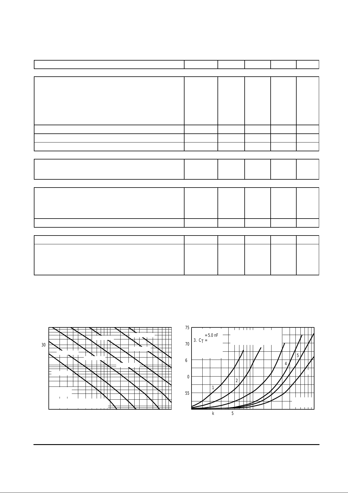
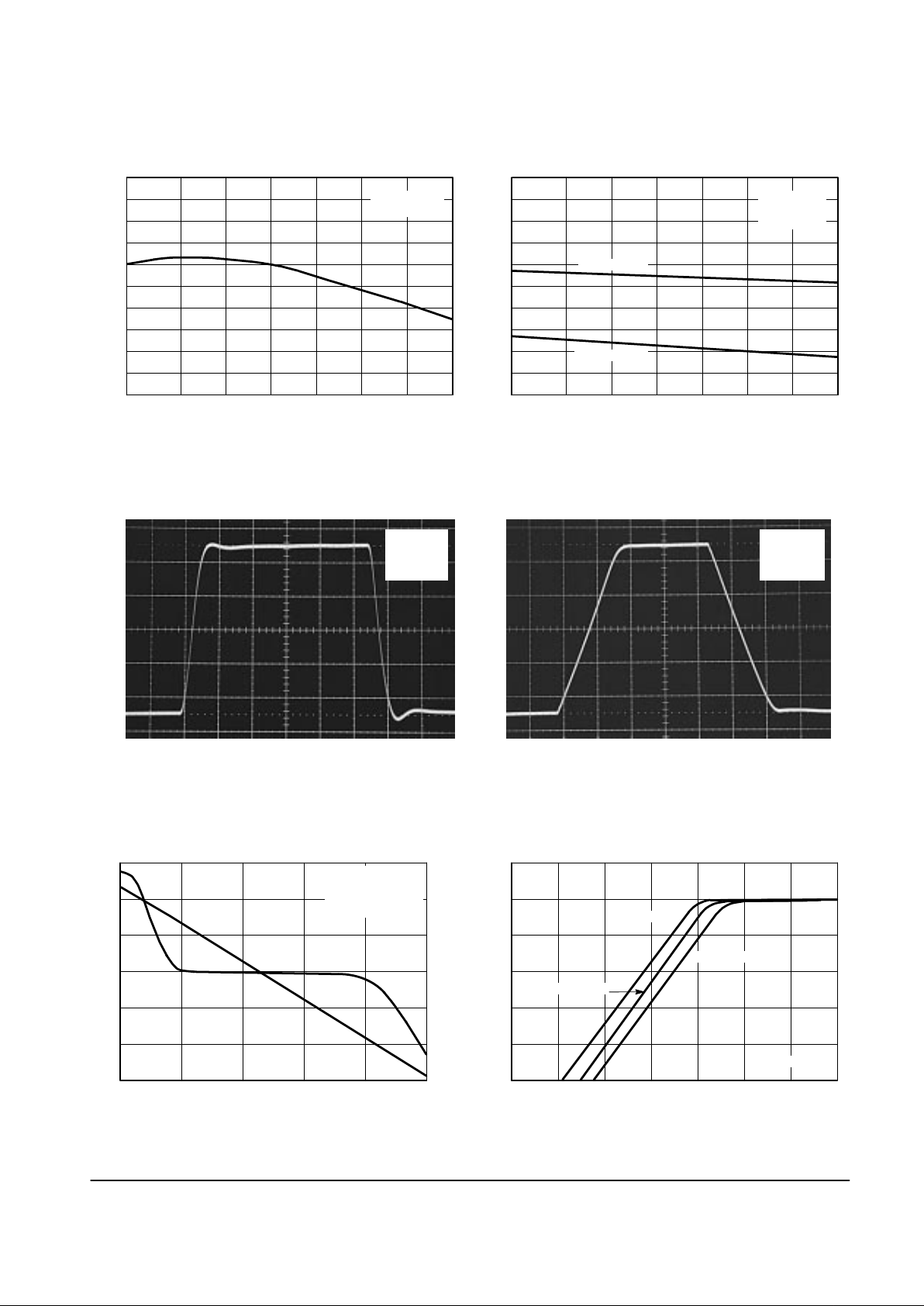
Figure 1. Timing Resistor
versus Oscillator Frequency
0.8
2.0
5.0
8.0
20
50
80
R
T
, TIMING RESISTOR (k )
Ω
1.0 M500 k200 k100 k50 k20 k10 k
f
OSC
, OSCILLATOR FREQUENCY (Hz)
CT=100 pF
CT=500 pF
Figure 2. Output Deadtime
versus Oscillator Frequency
1.0 M100 k10 k
f
OSC
, OSCILLATOR FREQUENCY (Hz)
50
% DT, PERCENT OUTPUT DEADTIME
1
2
3
4
5
55
60
65
70
75
Ä
6
30
10
3.0
1.0
20 k 50 k 200 k 500 k
Note: Output switches at
one–half the oscillator
frequency .
VCC = 12 V
TA = 25
°
C
CT=10 nF
CT=1.0 nF
CT=200 pF
CT=2.0 nF
VCC = 12 V
TA = 25
°
C
Note: Output switches at
one–half the oscillator frequency.
CT=5.0 nF
ÄÄÄÄ
ÄÄÄÄ
ÄÄÄÄ
1. CT = 10 nF
2. CT = 5.0 nF
3. CT = 2.0 nF
4. CT = 1.0 nF
5. CT = 500 pF
6. CT = 100 pF
MC44602
5
MOTOROLA ANALOG IC DEVICE DATA
OSC
Figure 3. Oscillator Discharge Current
versus Temperature
, DISCHARGE CURRENT (mA)
–55
TA, AMBIENT TEMPERATURE (
°
C)
–25 0 25 50 75 100 125
dischg
I
12
VCC = 12 V
V
OSC
= 3.0 V
Figure 4. Oscillator Voltage Swing
versus Temperature
–20
A
VOL
, OPEN LOOP VOL TAGE GAIN (dB)
10 M0.1 k
f, FREQUENCY (Hz)
Gain
Phase
0
30
60
90
120
150
180
1.0 k 10 k 100 k 1.0 M
0
20
40
60
80
100
EXCESS PHASSE (DEGREES)
Figure 5. Error Amp Small Signal
Transient Response
0
VO, ERROR AMP OUTPUT VOLTAGE (V)
0
, CURRENT SENSE INPUT THRESHOLD (V)V
th
0.2
0.4
0.6
0.8
1.0
1.2
2.0 4.0 6.0
VCC = 12 V
TA = 25°C
TA = 125°C
TA = –40°C
Figure 6. Error Amp Large Signal
Transient Response
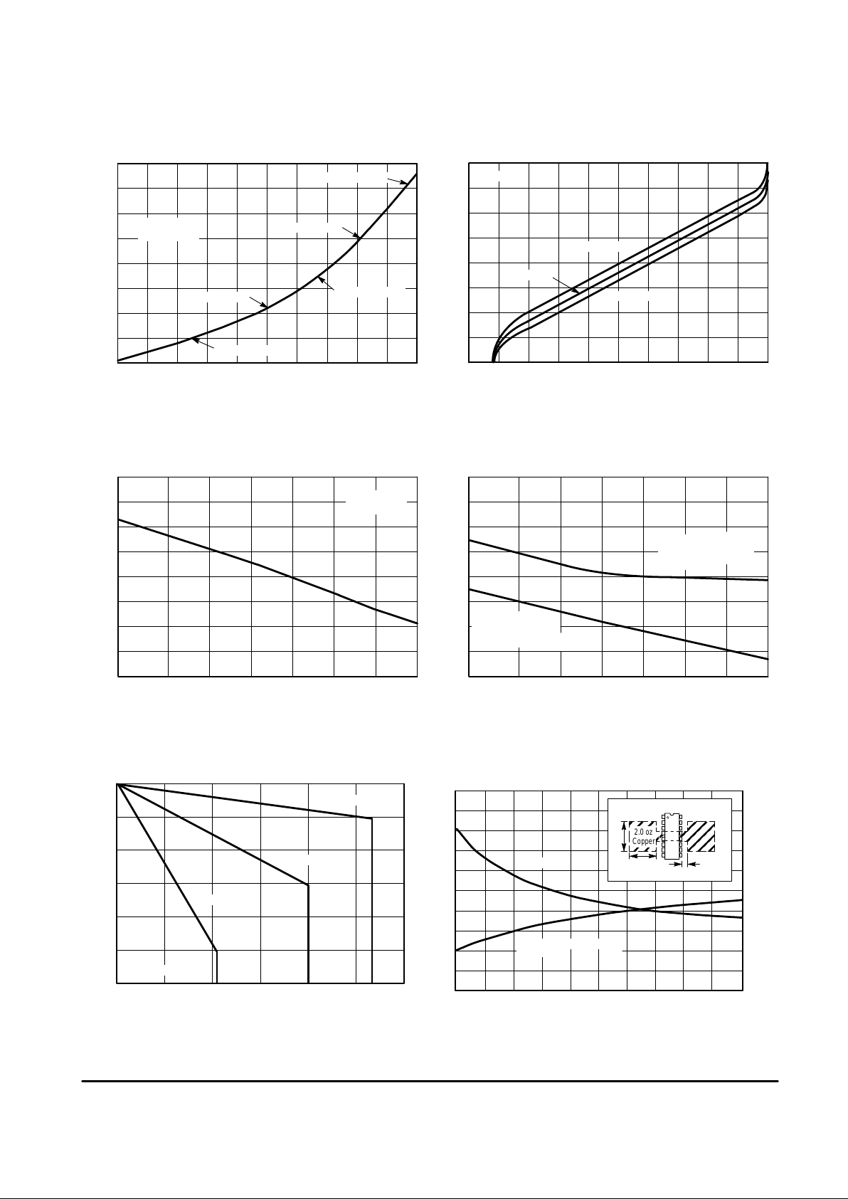
Figure 7. Error Amp Open Loop Gain and
Phase versus Frequency
Figure 8. Current Sense Input Threshold versus
Error Amp Output Voltage
, OSCILLATOR VOLTAGE SWING (V)V
5.0
4.0
3.0
2.0
1.0
0
–55
TA, AMBIENT TEMPERATURE (
°
C)
–25 0 25 50 75 100 125
VCC = 12 V
RT = 10 k
CT = 1.0 nF
Peak Voltage
Valley Voltage
1.0 3.0 5.0 7.0
11
10
9.0
8.0
7.0
VCC = 12 V
VO = 2.0 V to 4.0 V
RL = 100 k
TA = 25
°
C
2.55 V
2.5 V
2.45 V
3.0 V
2.5 V
2.0 V
t, TIME (0.5
µ
s/DIV) t, TIME (1.0 µs/DIV)
VCC = 12 V
AV = –1.0
TA = 25
°
C
VCC = 12 V
AV = –1.0
TA = 25
°
C
20 mV/DIV
200 mV/DIV
MC44602
6
MOTOROLA ANALOG IC DEVICE DATA
, REFERENCE VOLTAGE CHANGE (mV)
ref
V
∆
80
Figure 9. Voltage Feedback Input,
Voltage versus Current
0
0
100
R
JA
, THERMAL RESISTANCE JUNCTION TO AIR ( C/W)
θ
80
60
40
20
10 20 30 40 50
L, LENGTH OF COPPER (mm)
°
R
θ
JA
P
D
, MAXIMUM POWER DISSIPATION (W)
5.0
4.0
3.0
2.0
1.0
0
P
D(max)
for TA = 70°C
Figure 10. Voltage Feedback Input
versus Current Sense Clamp Level
Figure 11. Reference Short Circuit Current
versus Temperature
Figure 12. Reference Line and Load
Regulation versus Temperature
Figure 13. Reference Voltage Change
versus Source Current
Figure 14. Thermal Resistance and Maximum
Power Dissipation versus P.C.B. Copper Length
, INPUT VOLTAGE (V)
1.0
–500
Iin, INPUT CURRENT (
µ
A)
in
V
1.4
1.8
2.2
2.6
–400 –300 –200 –100 0
V
Clamp
= 1.0 V
V
Clamp
= 0.7 V
V
Clamp
= 0.3 V
VCC = 12 V
TA = 25
°
C
V
Clamp
= 0.1 V
V
Clamp
= 0.5 V
, INPUT VOLTAGE (V)
in
V
1.0
0
V
Clamp
, CURRENT SENSE CLAMP LEVEL (V)
1.4
1.8
2.2
2.6
0.2 0.4 0.6 0.8 1.0
TA = 125°C
VCC = 12 V
TA = –55°C
, REFERENCE SHORT CIRCUIT CURRENT (mA)
SC
I
40
–55
TA, AMBIENT TEMPERATURE (
°
C)
120
160
200
–25 0 25 50 75 100 125
VCC = 12 V
RL
≤
0.1
Ω
, REFERENCE VOLTAGE CHANGE (mA)
ref
V
3.0
–55
TA, AMBIENT TEMPERATURE (
°
C)
–25 0 25 50 75 100 125
∆
2.0
1.0
0
–1.0
–2.0
–3.0
–4.0
–5.0
Line Regulation
VCC = 12 V to 18 V
I
ref
= 0 mA
0
I
ref
, REFERENCE SOURCE CURRENT (mA)
0
30 60 90 120 150 180
–5.0
–10
–15
–20
–25
–30
TA = 125°C
TA = 25°C
TA = –55°C
Load Regulation
VCC = 12 V
I
ref
= 1.0 mA to 20 mA
TA = 25°C
VCC = 12 V
Graphs represent symmetrical layout
3.0 mm
Printed circuit board heatsink example
L
L
2.0 oz
Copper
 Loading...