

Motorola MC44461B Datasheet
SEMICONDUCTOR
TECHNICAL DATA
PICTURE–IN–PICTURE
(PIP) CONTROLLER
B SUFFIX
PLASTIC PACKAGE
CASE 859
(SDIP)
56
1
Order this document by MC44461/D
Device
Operating
Temperature Range
Package
ORDERING INFORMATION
MC44461B TJ = –65° to +150°C SDIP
For surface mount package availability, contact your local
Motorola sales office or authorized distributor.
1
MOTOROLA ANALOG IC DEVICE DATA
The MC44461 Picture–in–Picture (PIP) controller is a member of
Motorola’s low cost PIP family. It is NTSC compatible and contains all the
analog signal processing, control logic and memory necessary to provide for
the overlay of a small picture from a second non synchronized source onto
the main picture of a television. All control and setup of the MC44461 is via a
standard two pin I2C bus interface. The device is fabricated using BICMOS
technology. It is available in a 56–pin shrink dip (SDIP) package.
The main features of the MC44461 are:
• Two NTSC CVBS Inputs
• Switchable Main and PIP Video Signals
• Single NTSC CVBS Output Allows Simple TV Chassis Integration
• Two PIP Sizes; 1/16 and 1/9 Screen Area
• Freeze Field Feature
• V ariable PIP Position in 64–X by 64–Y Steps
• PIP Border with Programmable Color
• Programmable PIP Tint and Saturation Control
• Automatic Main to PIP Contrast Balance
• Vertical Filter
• Integrated 64 k Bit DRAM Memory Resulting in Minimal RFI
• Minimal RFI Allows Simple Low Cost Application into TV
• I
2
C Bus Control – No External Variable Adjustments Needed
• Operates from a Single 5.0 V Supply
• Economical 56–Pin Shrink DIP Package
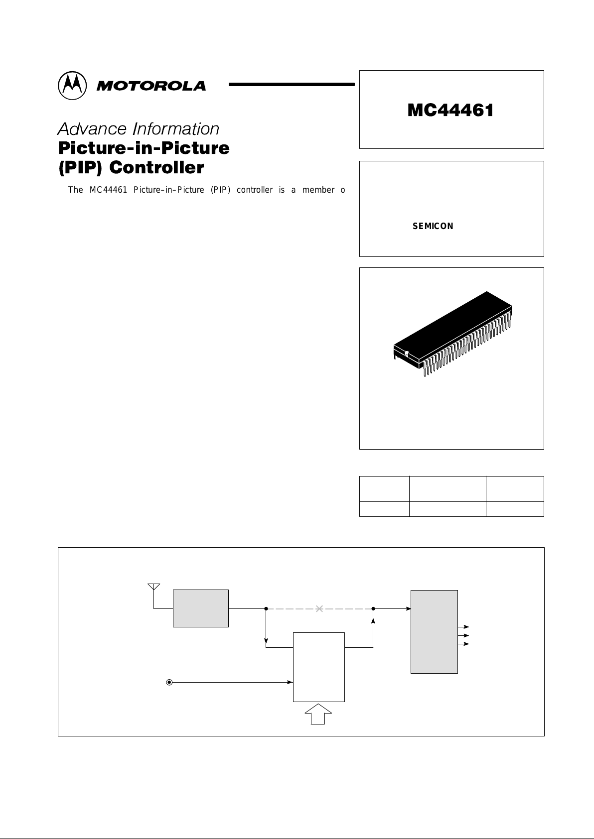
Composite Video Simplified System Diagram
Video
Processor
CV
1
PIP
MC44461
IIC
Tuner/IF
Back Panel
Composite
Video Input
R
G
B
CV
2
CV CV
in
This document contains information on a new product. Specifications and information herein
are subject to change without notice.
Motorola, Inc. 1996 Rev 0
MC44461
2
MOTOROLA ANALOG IC DEVICE DATA
MAXIMUM RATINGS
Rating Symbol Value Unit
Power Supply Voltage
V
DD
–0.5 to +6.0
V
Power Supply Voltage
V
CC
–0.5 to +6.0
V
ББББББББББББ
Á
Input Voltage Range
ÁÁ
Á
V
IR
ÁÁÁ
Á
–0.5,
V
DD
+ 0.5
Á
Á
V
Output Current
I
O
160
mA
Power Dissipation
Maximum Power Dissipation @ 70°C
P
D
1.3
W
Thermal Resistance, Junction–to–Air
R
θJA
59
°C/W
Junction T emperature (Storage and Operating)
T
J
–65 to +150
°C
NOTE: ESD data available upon request.
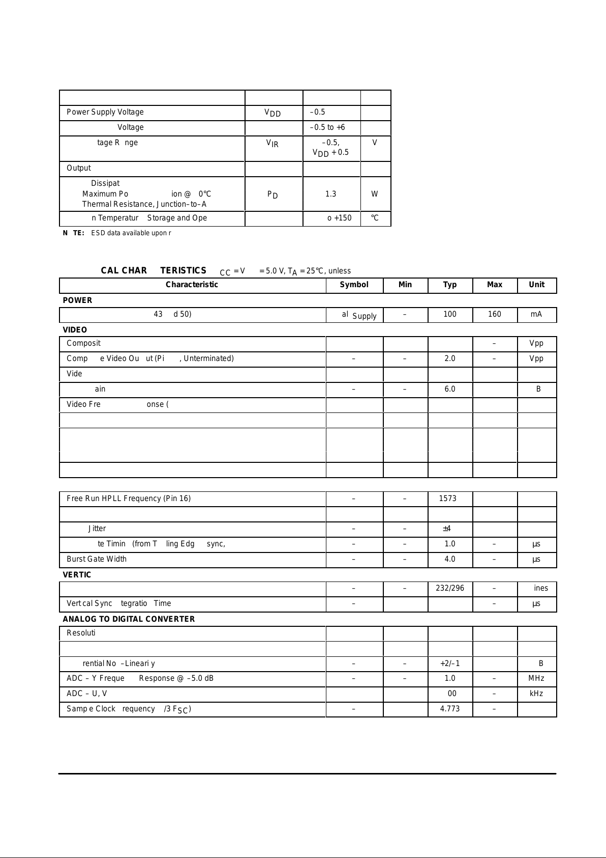
ELECTRICAL CHARACTERISTICS (V
CC
= VDD = 5.0 V , TA = 25°C, unless otherwise noted.)
Characteristic
Symbol Min Typ Max Unit
POWER SUPPLY
Total Supply (Pins 8, 15, 43 and 50)
Total I
Supply
–
100
160
ÁÁÁ
mA
VIDEO
Composite Video Input (Pin 34 or 36)
CVi
–
1.0
–
ÁÁÁ
Vpp
Composite Video Output (Pin 49, Unterminated)
–
–
2.0
–
ÁÁÁ
Vpp
Video Output DC Level (Sync Tip)
–
–
1.0
–
ÁÁÁ
Vdc
Video Gain
–
–
6.0
–
ÁÁÁ
dB
Video Frequency Response (Main Video to –1.0 dB)
–
–
10
–
ÁÁÁ
MHz
Color Bar Accuracy
–
–
±4.0
–
ÁÁÁ
deg
Video Crosstalk (@ 75% Color Bars)
–
ÁÁÁ
dB
Main to PIP
–
55
–
ÁÁÁ
PIP to Main
–
55
–
БББББББББББББББББ
Output Impedance
ÁÁÁ–ÁÁ–ÁÁ
5.0
ÁÁ
–
ÁÁÁ
ÁÁ
Ω
HORIZONTAL TIMEBASE
Free Run HPLL Frequency (Pin 16)
–
–
15734
–
ÁÁÁ
Hz
HPLL Pull–In Range
–
–
±400
–
ÁÁÁ
Hz
HPLL Jitter
–
–
±4.0
–
ÁÁÁ
ns
Burst Gate Timing (from Trailing Edge Hsync, Pin 24)
–
–
1.0
–
ÁÁÁ
µs
Burst Gate Width
–
–
4.0
–
ÁÁÁ
µs
VERTICAL TIMEBASE
Vertical Countdown Window
–
–
232/296
–
ÁÁÁ
H lines
Vertical Sync Integration T ime
–
–
31
–
ÁÁÁ
µs
ANALOG TO DIGITAL CONVERTER
Resolution
–
–
6
–
ÁÁÁ
Bits
Integral Non–Linearity
–
–
±1
–
ÁÁÁ
LSB
Differential Non–Linearity
–
–
+2/–1
–
ÁÁÁ
LSB
ADC – Y Frequency Response @ –5.0 dB
–
–
1.0
–
ÁÁÁ
MHz
ADC – U, V Frequency Response @ –5.0 dB
–
–
200
–
ÁÁÁ
kHz
Sample Clock Frequency (4/3 FSC)
–
–
4.773
–
ÁÁÁ
MHz
MC44461
3
MOTOROLA ANALOG IC DEVICE DATA
ELECTRICAL CHARACTERISTICS (continued) (V
CC
= VDD = 5.0 V , TA = 25°C, unless otherwise noted.)
Characteristic UnitMaxTypMinSymbol
DIGITAL TO ANALOG CONVERTER
Resolution
–
–
–
6
ÁÁÁ
Bits
Integral Non–Linearity
–
–
±1
–
ÁÁÁ
LSB
Differential Non–Linearity
–
–
+2/–1
–
ÁÁÁ
LSB
Tint DAC Control Range (in 64 Steps)
–
–
±10
–
ÁÁÁ
Deg
Saturation DAC Control Range (in 64 steps)
–
–
±6.0
–
ÁÁÁ
dB
NTSC DECODER
Color Kill Threshold
–
–
–24/–16
–
ÁÁÁ
dB
Threshold Hysteresis
–
–
3.0 ±1.0
–
ÁÁÁ
dB
ACC (Chroma Amplitude Change, +3.0 dB to –12 dB)
–
–
±0.5
–
ÁÁÁ
dB
PIP CHARACTERISTICS
PIP Size
–
ÁÁÁ
1/9 Screen Horizontal
–
114
–
ÁÁÁ
pels
1/9 Screen Vertical
–
71
–
ÁÁÁ
lines
1/16 Screen Horizontal
–
84
–
ÁÁÁ
pels
1/16 Screen Vertical
–
53
–
ÁÁÁ
lines
Border Size Horizontal
–
–
3
–
ÁÁÁ
pels
Border Size Vertical
–
–
2
–
ÁÁÁ
lines
Output PEL Clock (4 FSC)
–
–
14.318
–
ÁÁÁ
MHz
Position Control Range Horizontal (% of Main Picture), 64 Steps
–
–
100
–
ÁÁÁ
%
Position Control Range Vertical (% of Main Picture), 64 Steps
–
–
100
–
ÁÁÁ
%
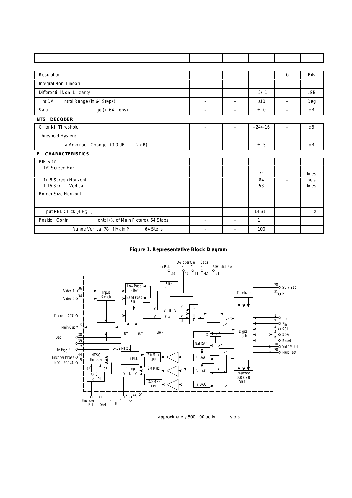
Figure 1. Representative Block Diagram
This device contains approximately 500,000 active transistors.
Y
V
U
YUV
Clamp
Input
Switch
Low Pass
Filter
Band Pass
Filter
NTSC
Decoder
PIP
Switch
4X S/C
Osc + PLL
16X S/C
Osc + PLL
YUV
Clamp
NTSC
Encoder
4X S/C
Osc + PLL
Filter
Tracking
6–Bit
ADC
H and V
Timebase
Digital
Logic
Memory
8.0 k x 8
DRAM
Tint DAC
Sat DAC
V DAC
Y DAC
3.0 MHz
LPF
3.0 MHz
LPF
3.0 MHz
LPF
33
Y
V
U
40 41 42 51
28
31
1
2
3
4
5
10
30
5453524746
6
6
6
6
6
3
6
Vert
57.28 MHz
90
°
0
°
14.32 MHz
90
°
0
°
36
34
37
49
38
39
7
44
45
Multiplexer
Video 1
Video 2
Decoder ACC
Main Out
Decoder Xtal
Decoder PLL
16 FSC PLL
Encoder Phase
Encoder ACC
Sync Sep
H PLL
H
in
V
in
SCL
SDA
Reset
Vid 1/2 Sel
Multi T est
Encoder Clamp Caps
Encoder
Xtal
Encoder
PLL
Decoder Clamp Caps
ADC Mid–RefFilter PLL
U DAC
MC44461
4
MOTOROLA ANALOG IC DEVICE DATA
0.1
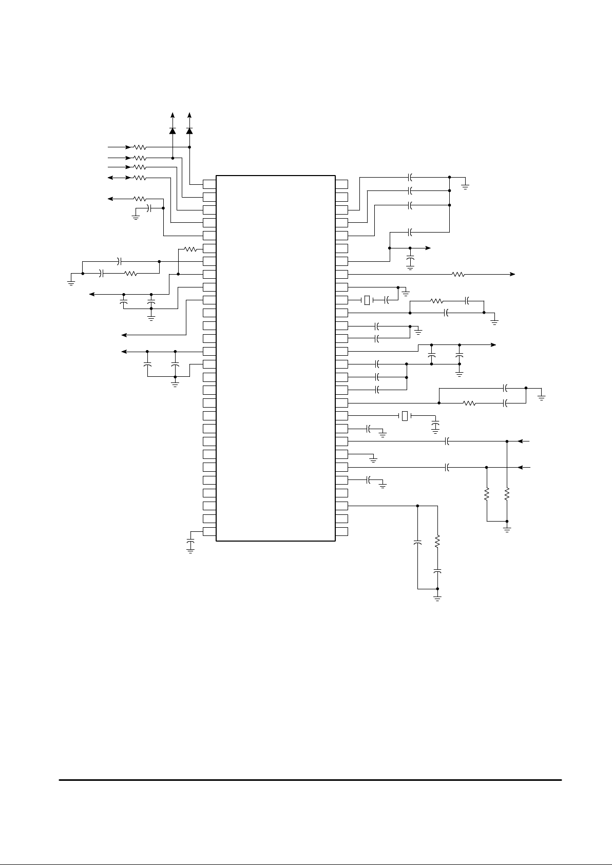
Figure 2. Application Circuit
40
39
38
37
36
35
34
33
46
45
44
43
42
41
32
31
30
29
48
47
56
55
54
53
52
51
50
49
1
2
3
4
5
6
9
10
11
12
13
14
15
16
7
8
17
18
19
20
21
22
23
24
25
26
27
28
N/C
N/C
N/C
N/C
N/C
N/C
N/C
N/C
VSS (dig)
Video 1/2 Select
N/C
N/C
N/C
VDD (mem)
VSS (mem)
N/C
H
in
V
in
SCL
SDA
Reset
Test Clk
16 FSC Filter
VDD (dig)
N/C
N/C
N/C
Sync Sep
Decoder PLL
Decoder Y Cap
Decoder Xtal
Decoder ACC
Video In 1
Analog Gnd
Video In 2
Filter PLL
Analog Gnd
Encoder Xtal
Encoder PLL
Encoder ACC
Encoder Phase
Analog V
CC
Decoder V Cap
Decoder U Cap
N/C
N/C
Encoder V Cap
Encoder U Cap
Endoder Y Cap
N/C
Video Out V
CC
Video Out
N/C
H PLL
Multi Test
N/C
0.01
0.01
0.01
0.1
µ
F
0.1
0.01
0.01
0.01
0.01
1000
100 k
75
X3
12
5.0 V
Video Out
5.0 V
2700
0.068
68 k
0.22
0.1
0.1
Video 1
Video 2
75 75
0.01
0.0068
12 k
1.0
µ
F
1.0
µ
F
5.0 V
Video 1/2
Select Out
1001000
100
2.2
µ
F
470 k
Horiz In
Vert In
I2C Ser Cl
I2C Ser Data
5.0 V
X2 – 14.31818 MHz – Fox 143–20 or equivalent
X3 – 14.31818 MHz – Fox 143–20 or equivalent
MC44461
NOTE: For proper noise isolation, Power Supply Pins 8, 14, 43 and 50 should be bypassed by both high and low
frequency capacitors. As a guideline, a 10 µF in parallel with a 0.1 µF at each supply pin is recommended.
0.0110 µF
5.0 V
0.0110 µF
0.01 10 µF
10 µF
X2
12
47 k
1.0 k
1.0 k
1.0 k
1.0 k
5.0 V 5.0 V

MC44461
5
MOTOROLA ANALOG IC DEVICE DATA
PIN FUNCTION DESCRIPTION
Pin Equivalent Internal Circuit Description
ÁÁÁ
Á
ÁÁÁ
Á
ÁÁÁ
Á
ÁÁÁ
Á
ÁÁÁ
Á
1
БББББББББББББ
ББББББББББББ
Á
ББББББББББББ
Á
ББББББББББББ
Á
ББББББББББББ
Á
ББББББББББББ
Á
1
1.0 k
ББББББББББББББББ
Á
ББББББББББББББББ
Á
ББББББББББББББББ
Á
ББББББББББББББББ
Á
ББББББББББББББББ
Á
Horizontal Reference In (Hin)
CMOS level pulse synchronous with TV horizontal retrace signal. This
pulse may be active high or low since there is a polarity selector bit in
an internal control register.
This pulse should begin 0.5 to 0.75 µs after
the beginning of the main video H sync period.
Its duty cycle should be
less than 50%.
ÁÁÁ
Á
ÁÁÁ
Á
ÁÁÁ
Á
ÁÁÁ
Á
2
БББББББББББББ
ББББББББББББ
Á
ББББББББББББ
Á
ББББББББББББ
Á
ББББББББББББ
Á
2
1.0 k
ББББББББББББББББ
Á
ББББББББББББББББ
Á
ББББББББББББББББ
Á
ББББББББББББББББ
Á
Vertical Reference In (Vin)
CMOS level pulse synchronous with TV vertical retrace signal. This
pulse may be active high or low since there is a polarity selector bit in
an internal control register. This pulse should begin during the main
video vertical interval and have a duration of at least .5H.
ÁÁÁ
Á
ÁÁÁ
Á
ÁÁÁ
Á
ÁÁÁ
Á
3
3
1.0 k
ББББББББББББББББ
Á
ББББББББББББББББ
Á
ББББББББББББББББ
Á
ББББББББББББББББ
Á
Serial Clock (SCL)
CMOS level I2C Compatible slave only clock input. 100 kHz Maximum
frequency. 50% duty cycle. See Figure 4 for timing. See I2C Register
Description for internal register descriptions and addresses.
ÁÁÁ
Á
ÁÁÁ
Á
ÁÁÁ
Á
ÁÁÁ
Á
ÁÁÁ
Á
4
4
1.0 k
ББББББББББББББББ
Á
ББББББББББББББББ
Á
ББББББББББББББББ
Á
ББББББББББББББББ
Á
ББББББББББББББББ
Á
Serial Data (SDA)
CMOS level I2C Compatible slave only data input/output. As an output
it is open collector. See Figure 4 for timing. See I2C Register
Description for internal register descriptions and addresses.
ÁÁÁ
Á
ÁÁÁ
Á
ÁÁÁ
Á
ÁÁÁ
Á
ÁÁÁ
Á
5
БББББББББББББ
ББББББББББББ
Á
ББББББББББББ
Á
ББББББББББББ
Á
ББББББББББББ
Á
ББББББББББББ
Á
5
470 k
2.2 µF
5.0
ББББББББББББББББ
Á
ББББББББББББББББ
Á
ББББББББББББББББ
Á
ББББББББББББББББ
Á
ББББББББББББББББ
Á
Reset
The active low, Power On Reset initializes all internal registers to zero
and resets the I2C interface. Minimum active low time required for
Power On Reset reset is 100 ms.
ÁÁÁ
Á
ÁÁÁ
Á
ÁÁÁ
Á
ÁÁÁ
Á
ÁÁÁ
Á
6
БББББББББББББ
ББББББББББББ
Á
ББББББББББББ
Á
ББББББББББББ
Á
ББББББББББББ
Á
ББББББББББББ
Á
6
47 k
5.0
ББББББББББББББББ
Á
ББББББББББББББББ
Á
ББББББББББББББББ
Á
ББББББББББББББББ
Á
ББББББББББББББББ
Á
Test Clock
ÁÁÁ
Á
ÁÁÁ
Á
ÁÁÁ
Á
ÁÁÁ
Á
ÁÁÁ
Á
ÁÁÁ
Á
ÁÁÁ
7
БББББББББББББ
ББББББББББББ
Á
ББББББББББББ
Á
ББББББББББББ
Á
ББББББББББББ
Á
ББББББББББББ
Á
ББББББББББББ
Á
ББББББББББББ
7
100 1000
100
ББББББББББББББББ
Á
ББББББББББББББББ
Á
ББББББББББББББББ
Á
ББББББББББББББББ
Á
ББББББББББББББББ
Á
ББББББББББББББББ
Á
ББББББББББББББББ
PLL Filter
Filter for the 16X S/C PLL which is phase locked to the 4X S/C
oscillator.
Pins 11 to 13, 16 to 27, 55 and 56 are test pins configured as outputs in a high impedance state. In an application, no connection should be made to these pins.
 Loading...