Motorola MC44302ADW Datasheet
Device
Tested Operating
Temperature Range
Package
SEMICONDUCTOR
TECHNICAL DATA
ADVANCED
MULTI–STANDARD
VIDEO/SOUND IF
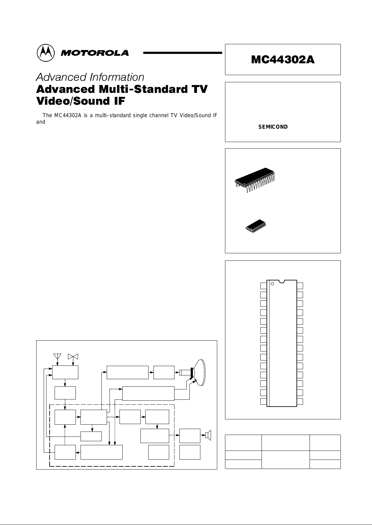
ORDERING INFORMATION
MC44302ADW
MC44302AP
TA = 0° to +70°C
SO–28L
Plastic DIP
P SUFFIX
PLASTIC PACKAGE
CASE 710
28
1
(Top View)
PIN CONNECTIONS
Order this document by MC44302A/D
28
1
DW SUFFIX
PLASTIC PACKAGE
CASE 751F
(SO–28L)
1
2
3
4
5
6
7
8
9
10
11
12
13
14
28
27
26
25
24
23
22
21
20
19
18
17
16
15
Intercarrier
Sound Output
DC Volume Control
Sound Input (FM)
Audio Input/
Audio–Video Switch
Sound
De–Emphasis (FM)
Negative Video Out
Positive Video Out
Sound AFT Filter/
Peak White Filter
Video IF Input
Video IF Input
Video Mode Switch
AFT Output
AFT Mode Switch
RF AGC Output
Video IF AGC Filter
Audio Output
(Variable)
Sound Quadrature
Coil (FM)
V
CC
Audio Output
(Constant)
Sound Input (AM)
Gnd
VCO Coil
VCO Coil
PLL Filter
(Main VCO Loop)
Lock Detector/Filter
(Acquisition Circuit)
Flyback/Video Input
Horizontal PLL Filter
RF AGC Delay
1
MOTOROLA ANALOG IC DEVICE DATA
The MC44302A is a multi–standard single channel TV Video/Sound IF
and PLL detector system specifically designed for use with all standard
modulation techniques including NTSC, PAL, and SECAM. This device
enables the designer to produce a high quality IF system with a minimum
number of external components.
The MC44302A contains a high gain video IF with an AGC range of 80 dB,
enhanced phase–locked loop carrier regenerator for low static phase error,
doubly balanced full wave synchronous video demodulator featuring wide
bandwidth positive and negative video outputs with extremely low differential
gain and phase distortion, video AFT amplifier, multistage sound IF limiter
with FM quadrature detector and AFT for self tuning, AM sound detector,
constant and variable audio outputs, dc volume control for reduced hum and
noise pickup, unique signal acquisition circuit that prevents false PLL lockup
and AFT push out, horizontal gating system with sync separator and
phase–locked loop circuitry for self–contained RF/IF AGC operation, RF
AGC delay circuitry, and programmable control logic that allows operation in
NTSC, and PAL SECAM systems. This device is available in wide body 28 pin
dual–in–line and surface mount plastic packages.
• Multi–Standard Detector System for NTSC, PAL, and SECAM
• High Gain Video IF Amplifier with 80 dB AGC Range
• Enhanced PLL Carrier Regenerator for Low Static Phase Error
• Synchronous Video Demodulator with Positive and Negative Video
Outputs
• Sound IF with Self Tuning FM Quadrature Detector
• AM Sound Detector
• DC Volume Control
• Unique Signal Acquisition Circuit Prevents False PLL Lockup
• Horizontal Gating System for Self Contained RF/IF AGC Operation
• RF AGC Delay Circuitry
This document contains information on a new product. Specifications and information herein
are subject to change without notice.
Motorola, Inc. 1997 Rev 0
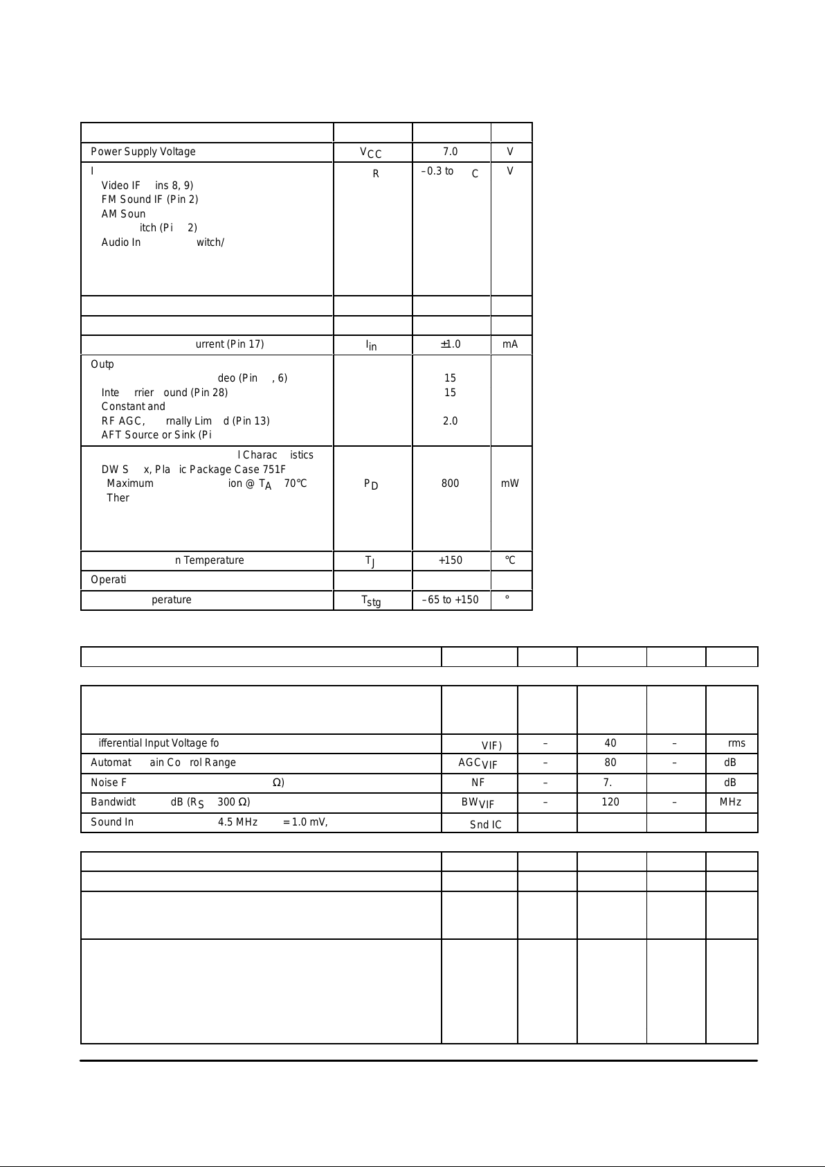
Simplified Television Block Diagram
DC Volume
Control
MC44302A
Vertical & Horizontal
Scan Circuitry
Power
Supply
VHF/UHF
Tuner
Video
IF
Audio
Amp
Video
Detector
Sound
IF
Sound
Detector
Video
Drivers
Luma & Chroma
Processor
SAW
Filter
Horizontal
Gating System
RF/IF
AGC
Mode
Switch
AFT
MC44302A
2
MOTOROLA ANALOG IC DEVICE DATA
MAXIMUM RATINGS
Rating Symbol Value Unit
Power Supply Voltage
V
CC
7.0
V
Input Voltage Range
V
IR
–0.3 to V
CC
V
Video IF (Pins 8, 9)
FM Sound IF (Pin 2)
AM Sound IF (Pin 23)
AFT Switch (Pin 12)
Audio Input/Audio Switch/Video Invert (Pin 3)
Mode Switch (Pin 10)
RF AGC Delay (Pin 15)
Volume Control (Pin 1)
Sound Quadrature Coil Voltage (Pin 26)
V
QC
V
CC
V
VCO Coil Voltage (Pins 20, 21)
V
VCO
V
CC
V
Flyback/Video Input Current (Pin 17)
I
in
±1.0
mA
Output Current
I
O
mA
Positive and Negative Video (Pins 5, 6) 15
Intercarrier Sound (Pin 28) 15
Constant and Variable Audio (Pins 24, 27) 15
RF AGC, Internally Limited (Pin 13) 2.0
AFT Source or Sink (Pin 11) 4.0
Power Dissipation and Thermal Characteristics
DW Suffix, Plastic Package Case 751F
Maximum Power Dissipation @ T
A
= 70°C P
D
800 mW
Thermal Resistance, Junction–to–Air R
θJA
100 °C/W
P Suffix, Plastic Package Case 710
Maximum Power Dissipation @ T
A
= 70°C P
D
1000 mW
Thermal Resistance, Junction–to–Air R
θJA
80 °C/W
Operating Junction Temperature
T
J
+150
°C
Operating Ambient Temperature
T
A
0 to +70
°C
Storage Temperature
T
stg
–65 to +150
°C
NOTE: ESD data available upon request.
ELECTRICAL CHARACTERISTICS (V
CC
= 5.0 V , TA = 25°C.)
Characteristic
Symbol Min Typ Max Unit
VIDEO IF AMPLIFIER
Differential Input Impedance Components
Parallel Resistance R
in(VIF)
– 3.4 – kΩ
Parallel Capacitance C
in(VIF)
– 4.0 – pF
Differential Input V oltage for Full Video Output Swing DV
in(VIF)
– 40 – µVrms
Automatic Gain Control Range AGC
VIF
– 80 – dB
Noise Figure (Vin = 1.0 mV, RS = 300 Ω) NF – 7.0 – dB
Bandwidth, –3.0 dB (RS = 300 Ω) BW
VIF
– 120 – MHz
Sound Intercarrier Output, 4.5 MHz (Vin = 1.0 mV , Note 2) V
O(Snd IC)
– 0.1 – Vrms
VIDEO DETECTOR
Output Voltage Swing (Pin 5 or 6, RL = 2.0 k, Note 1) V
O(VD)
– 2.2 – Vpp
Output Impedance (Pin 5 or 6, 1.0 MHz, 1.0 mA) |ZO| – 100 – Ω
Bandwidth, –3.0 dB, (RL = 2.0 k) BW
VD
MHz
Negative Output (Pin 5) – 8.0 –
Positive Output (Pin 6) – 7.0 –
Output Distortion, Uncorrected (RL = 2.0 k, Note 1)
Differential Gain DG %
Negative Video Output – 2.0 5.0
Positive Video Output – 2.0 5.0
Differential Phase DP Deg
Negative Video Output – 1.0 5.0
Positive Video Output – 1.0 5.0

MC44302A
3
MOTOROLA ANALOG IC DEVICE DATA
ELECTRICAL CHARACTERISTICS (continued) (V
CC
= 5.0 V , TA = 25°C.)
Characteristic UnitMaxTypMinSymbol
VIDEO DETECTOR (CONTINUED)
Residual 920 kHz Beat Output, dB Below 100% Modulated Video B
O
– –60 – dB
(Pin 5 or 6, Note 2)
FM SOUND IF AND DETECTOR
Input Impedance Components
Parallel Resistance R
in(FM)
– 2.2 – kΩ
Parallel Capacitance C
in(FM)
– 4.0 – pF
Input Limiting Threshold (f = 4.5 MHz) V
in(Snd)
– 80 – µV
AM Rejection (Vin = 10 mV, Notes 4, 5, 6) AMR dB
f = 4.5 MHz – 50 –
f = 5.5 MHz – 50 –
Recovered Audio Output (Pin 24, Vin = 10 mV , Note 4) V
O(Snd)
Vpp
f = 4.5 MHz – 2.0 –
f = 5.5 MHz – 2.0 –
Output Distortion (Pin 24, Vin = 10 mV , Note 4) THD %
f = 4.5 MHz – 1.0 –
f = 5.5 MHz – 1.0 –
Sound AFT (Note 7) ∆f
AFT(Snd)
MHz
Pull–in Range – ±0.6 –
Hold–in Range – ±0.6 –
Sound De–Emphasis Internal Resistance (Pin 4) R
DE
– 18 – kΩ
AM Detector Crosstalk Ctlk
AM
– –6.0 – dB
AM DETECTOR
Input Impedance Components
Parallel Resistance R
in(AM)
– 5.6 – kΩ
Parallel Capacitance C
in(AM)
– 4.0 – pF
Recovered Audio Output (Pin 24, Vin = 100 mV , Note 5) V
O(Snd)
– 2.0 – Vpp
Output Distortion (Pin 24, Vin = 10 mV , Note 5) THD – 1.0 – %
FM Sound IF and Detector Crosstalk Ctlk
FM
– –60 – dB
DC VOLUME CONTROL
Volume Control Range (Pin 1, Pin 3 = Vin) ∆V
O(Snd)
– +12 to –70 – dB
Output Signal at Minimum Volume Setting (Pin 1 = Gnd, Pin 3 = Vin ) V
O(Snd)
– 1.0 – mV
Video Detector Sync to Audio Channel Crosstalk Ctlk
VD
dB
Fixed Output – –60 –
Variable Output – –60 –
Audio Channel Crosstalk Ctlk
Snd
dB
Fixed Output to Variable Output – –60 –
Variable Output to Fixed Output – –60 –
NOTES: 1. V
in
= 1.0 mVrms signal at 45.75 MHz with 75% modulated staircase at 3.58 MHz.
2.Vin = 100 µVrms signal at 41.25 MHz added to signal in Note 1.
3.Differential carrier level at video IF inputs to cause the negative detector output to go positive by 0.1 V from ground.
4.FM Modulation = ±25 kHz deviation at 1.0 kHz for 4.5 MHz intercarrier.
±50 kHz deviation at 1.0 kHz for 5.5 MHz intercarrier.
5.AM Modulation = 30% depth at 1.0 kHz for 4.5 MHz and 5.5 MHz intercarrier.
6.AM Rejection (dB) = 20 log
7.Tested with 15 µH sound quadrature coil in parallel with 68 pF and 10 kΩ.
8.The AFT output can be disabled by leaving Pin 12 disconnected or by biasing it to the voltage level shown above. When disabled, the output will be
internally clamped to one half of VCC.
V
O(FM)
V
O(AM)

MC44302A
4
MOTOROLA ANALOG IC DEVICE DATA
ELECTRICAL CHARACTERISTICS
(continued) (VCC = 5.0 V , TA = 25°C.)
Characteristic UnitMaxTypMinSymbol
PHASE–LOCKED LOOP
Acquisition Circuit Filter Voltage (Pin 18) V
PLL(Acq)
V
Unlocked with No–Signal – 2.7 –
Unlocked to Locked Sweep Range upon Signal Acquisition – 1.2 to 4.3 –
Locked, Final Static Condition – 4.3 –
VCO Filter Voltage (Pin 19) V
PLL(VCO)
V
Unlocked – 3.2 –
Locked, Final Static Condition – 3.2 –
Video IF Lock–Up Time t
IF(lock)
– 5.0 – ms
HORIZONTAL GATING SYSTEM
Sync Separator Input Threshold Voltage (Pin 17) V
th(Sync)
– 3.4 – V
PLL Filter Voltage, Locked or Unlocked with No–Signal (Pin 16) V
PLL(Horiz)
– 2.9 ± 1.1 – V
RF AGC
RF AGC Delay Voltage Range (Pin 15) V
AGC(DLY)
– 1.7 to 2.4 – V
RF AGC Output Current (Pin 13) I
O(sink)
1.0 2.0 – mA
LOGIC CONTROL
Mode Select Voltage Range (Pin 10) V
th(Mode)
V
PAL 1 4.7 to 5.0 4.6 to 5.0 –
PAL 2 3.5 to 4.1 3.4 to 4.2 –
SECAM 2.3 to 2.9 2.2 to 3.0 –
NTSC 0 to 0.3 0 to 0.4 –
AFT Switch Threshold (Pin 12) V
th(AFT)
AFT Output, Pin 11, Sourcing when IF Frequency is Low – 5.0 –
AFT Output, Pin 11, Sinking when IF Frequency is Low – 0 –
AFT Output, Pin 11, Disabled (Note 8) – 2.5 –
Audio Switch/Video Invert V oltage Range (Pin 3) V
th(AS/VI)
V
Audio 1, Internal Audio (AM or FM) appears at Pins 24 and 27, 3.4 to 5.0 3.3 to 5.0 –
Positive Video appears at Pin 6,
Negative Video appears at Pin 5
Audio 2, Internal Audio (AM or FM) appears at Pin 24, 1.8 to 2.2 1.7 to 2.3 –
External Audio appears at Pin 27,
Positive Video appears at Pin 6,
Negative Video appears at Pin 5
Video 1, Internal Audio (AM or FM) appears at Pins 24 and 27, 0.6 to 0.9 0.5 to 1.0 –
Positive Video appears at Pin 6,
Negative Video appears at Pin 5
Video 2, Internal Audio (AM or FM) appears at Pins 24 and 27, 0 to 0.2 0 to 0.3 –
Positive Video appears at Pin 5,
Negative Video appears at Pin 6
TOTAL DEVICE
Operating Voltage V
CC
V
TA = 25°C 4.5 5.0 5.5
TA = 0°C to 70°C 4.75 – 5.5
Power Supply Current (VCC = 5.0 V) I
CC
– 100 – mA
NOTES: 1. V
in
= 1.0 mVrms signal at 45.75 MHz with 75% modulated staircase at 3.58 MHz.
2.Vin = 100 µVrms signal at 41.25 MHz added to signal in Note 1.
3.Differential carrier level at video IF inputs to cause the negative detector output to go positive by 0.1 V from ground.
4.FM Modulation = ±25 kHz deviation at 1.0 kHz for 4.5 MHz intercarrier.
±50 kHz deviation at 1.0 kHz for 5.5 MHz intercarrier.
5.AM Modulation = 30% depth at 1.0 kHz for 4.5 MHz and 5.5 MHz intercarrier.
6.AM Rejection (dB) = 20 log
7.Tested with 15 µH sound quadrature coil in parallel with 68 pF and 10 kΩ.
8.The AFT output can be disabled by leaving Pin 12 disconnected or by biasing it to the voltage level shown above. When disabled, the output will be
internally clamped to one half of VCC.
V
O(FM)
V
O(AM)
MC44302A
5
MOTOROLA ANALOG IC DEVICE DATA
f
offset
, OFFSET CHANGE (kHz)
∆
VCC, SUPPLY VOLTAGE (V)
4.5
100
1.4
1000
41
1000
0.01
2.5
f
VCO
, FREE–RUNNING CHANGE (kHz)
∆
CARRIER DIFFERENTIAL INPUT VOLT AGE (mV rms)
RF AGC TAKEOVER THRESHOLD, PIN 15 (V)
CARRIER DIFFERENTIAL INPUT VOLT AGE (mV rms)
CARRIER FREQUENCY (MHz)
IF AGC FILTER VOLT AGE, PIN 14 (V)
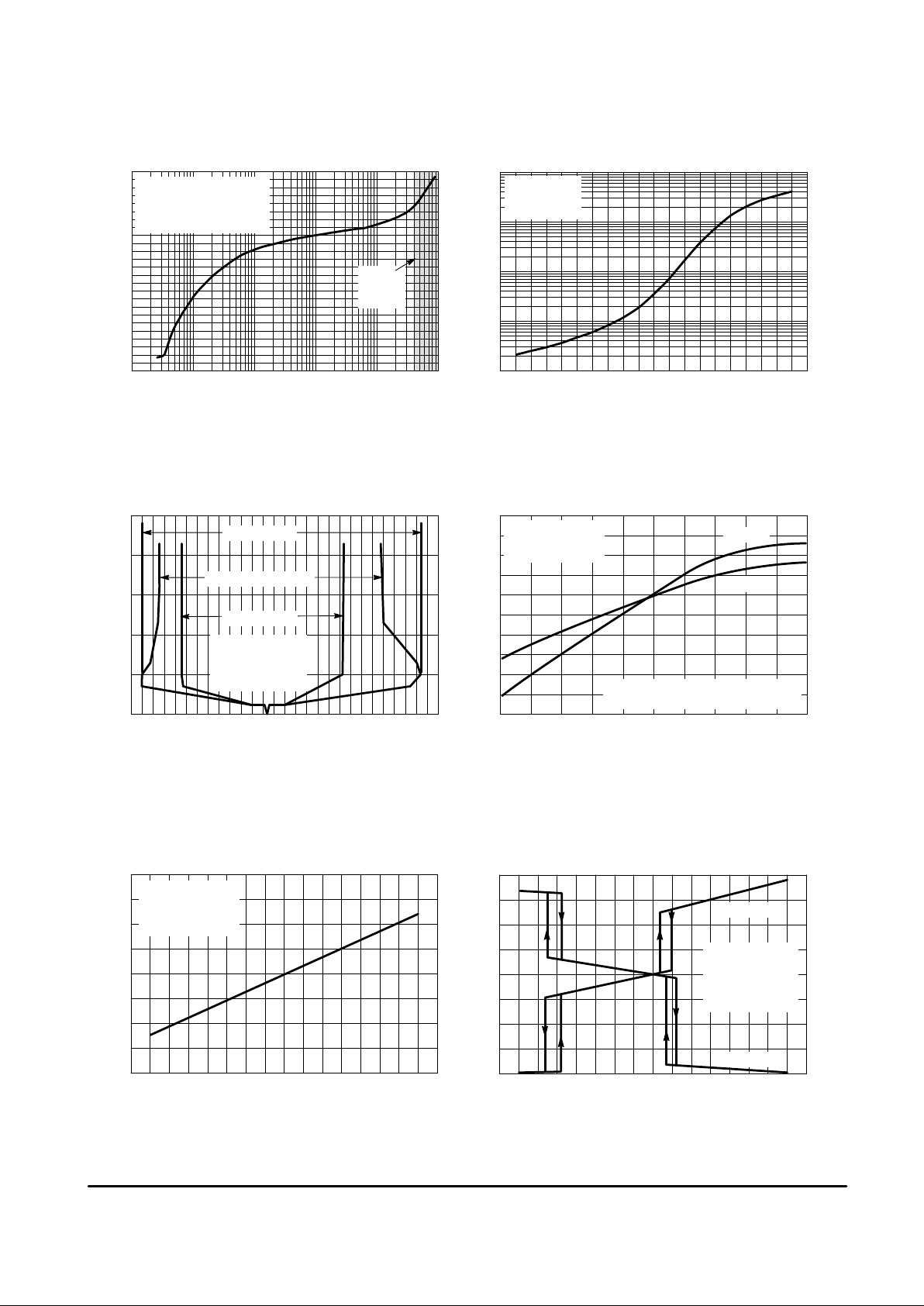
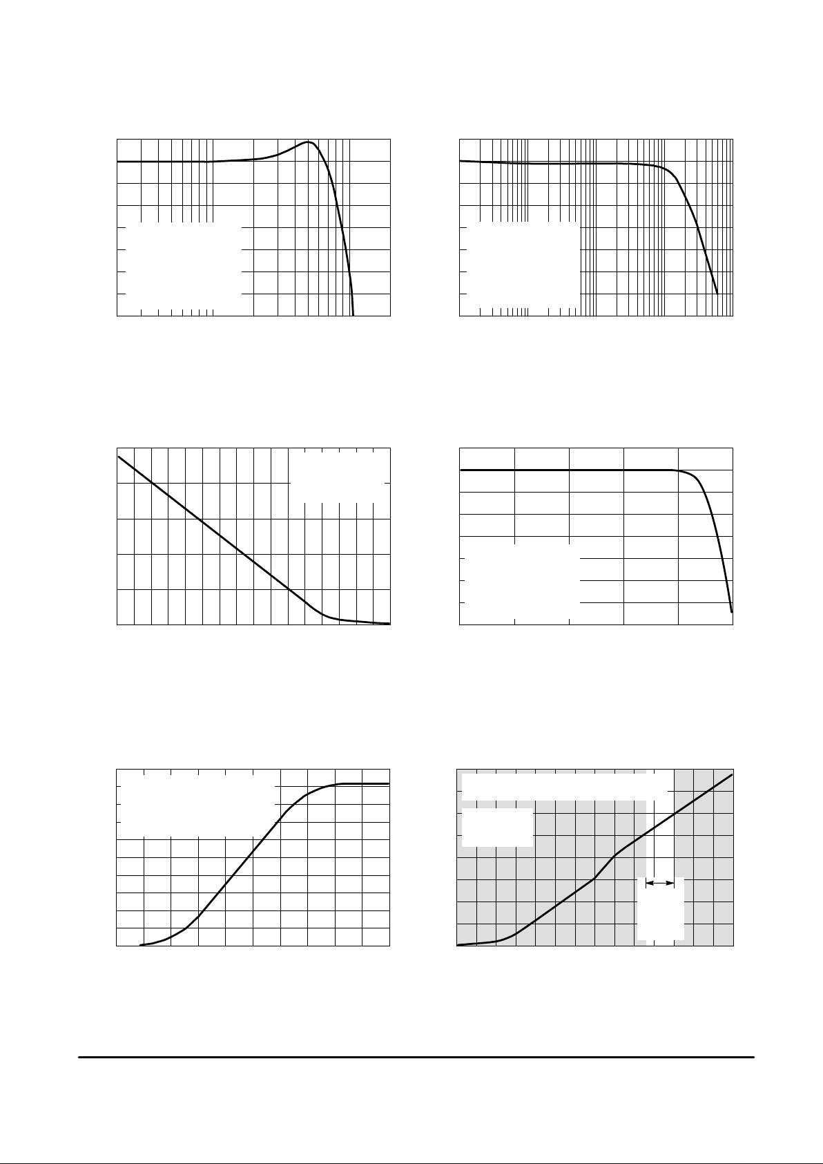
Figure 1. IF AGC Filter Voltage versus
Carrier Differential Input Voltage
CARRIER DIFFERENTIAL INPUT VOL TAGE (mVrms)
Figure 2. Carrier Differential Input Voltage versus
RF AGC Takeover Threshold
VCC = 5.0 V
fC = 45.75 MHz
RF AGC Delay, Pin 15, Open
TA = 25
°
C
Figure 3. VCO Characteristics
Figure 4. VCO Free–Running and Offset
Frequency Change versus Supply Voltage
0.1 1.0 10 100 1000 1.6 1.8 2.0 2.2 2.4
42 43 44 45 46 47 4.7 4.9 5.1 5.3 5.548
2.0
1.5
1.0
0.5
0
100
10
1.0
0.1
100
10
1.0
0.1
0.01
50
0
–50
–100
–150
100
50
0
–50
–100
–150
VCC = 5.0 V
fC = 45.75 MHz
TA = 25
°
C
VCC = 5.0 V
f
VCO
= 22.875 MHz
C19, C20 = 33 pF
TA = 25
°
C
f
VCO
= 22.875 MHz
C19, C20 = 33 pF
TA = 25
°
C
∆
f
offset
∆
f
VCO
Readings are taken at five minute intervals
allowing the die temperature to stabilize.
Input
Overload
Region
Lock–In Range
Sweep Capture Range
Hold–In Range
PLL FILTER VOLTAGE, PIN 19 (V)
CARRIER FREQUENCY CHANGE (MHz)
–2.0
2.0
–2.0
4.8
AFT OUTPUT CURRENT, PIN 11 (mA)
Figure 5. PLL Filter Voltage versus
Carrier Frequency Change
CARRIER FREQUENCY CHANGE (MHz)
Figure 6. AFT Output Current
versus Carrier Frequency Change
VCC = 5.0 V
f
VCO
= 22.875 MHz
C19, C20 = 33 pF
TA = 25
°
C
Pin 12 = Gnd
VCC = 5.0 V
f
VCO
= 22.875 MHz
C19, C20 = 33 pF
Pin 11 = 2.5 V
TA = 25
°
C
Pin 12 = V
CC
4.0
2.4
3.2
1.6
1.0
0
–1.0
–2.0
–1.0 0 1.0 2.0 –1.0 0 1.0 2.0
MC44302A
6
MOTOROLA ANALOG IC DEVICE DATA
10
7.0
1.0
20
0
0
SELF–TUNING FREQUENCY RANGE (MHz)
EXTERNAL TANK CAPACITANCE, C25 (pF)
INTERNAL TUNING CAPACITANCE, PIN 26 (pF)
SOUND AFT FILTER VOLTAGE, PIN 7 (V)
RELATIVE DETECTED VIDEO OUTPUT (dB)
VIDEO MODULATION FREQUENCY (MHz)
Figure 7. Video Output Frequency Response
–4.0
–8.0
–12
–16
–20
16
12
8.0
4.0
0
6.0
5.0
4.0
4.0 8.0 12 16
2.0 3.0 4.0 50 60 70 100
VCC = 5.0 V
TA = 25
°
C
Parasitic layout and
coil capacitance
must be considered.
VCC =
5.0 V
R28 = 10 k
Pin 7 = 1.5 V to 3.8 V
Vin = 500
µ
Vrms into Pin 2
Mod =
±
25 kHz Dev at 1.0 kHz
TA = 25
°
C
L3 =
10
µ
H
15 20 30 40
L3 =
15 µH
80
Negative Video
Output Pin 5
VCC = 5.0 V
fC = 45.75 MHz
TA = 25
°
C
0.1
RELATIVE OUTPUT, PINS 24, 27 (dB)
INTERCARRIER MODULATION FREQUENCY, PIN 2 (kHz)
RELATIVE OUTPUT, PINS 24, 27 (dB)
INTERCARRIER INPUT VOLTAGE, PIN 2 (mVrms)
–10
–20
–30
–40
–50
–60
–70
–80
1.0 10 100
1000
C4 =
3.3 nF
C4 =
1.0 nF
C4 =
0 pF
C4 =
100 pF
L3 =
22
µ
H
6.5
5.5
4.5
3.5
VCC = 5.0 V
fC = 5.5 MHz
Mod =
±
50 kHz Dev at 1.0 kHz
0 dB Output Level = 0.45 Vrms
TA = 25
°
C
Output
Level
S
)
N
N
VCC = 5.0 V
PAL 1 Mode Selected
Vin = 10 mVrms into Pin 2
fC = 4.5 MHz
Dev =
±
25 kHz
RL = 10 M
Ω
CL = 10 pF
TA = 25
°
C
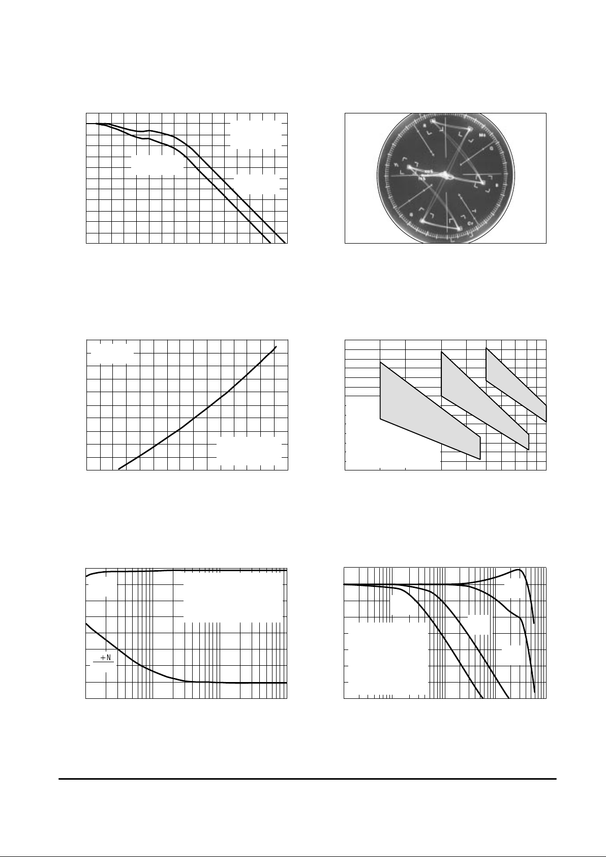
Figure 8. Vectorscope Display of
75% Saturated NTSC Color Bars
Figure 9. FM Sound AFT Filter Voltage
versus Internal Tuning Capacitance
Figure 10. FM Sound Intercarrier Self–Tuning
Frequency Range versus External Tank Capacitance
Figure 11. FM Sound Detector Relative Output, and
Signal to Noise Ratio versus Intercarrier Input Voltage
Figure 12. FM Sound Detector Frequency Response
Picture taken
without Figure 27
correction circuit
0
0.1 1.0 10 100
0
–4.0
–8.0
–12
–16
–20
–24
–28
4.0
VCC = 5.0 V
fC = 45.75 MHz
TA = 25
°
C
Positive Video
Output Pin 6
MC44302A
7
MOTOROLA ANALOG IC DEVICE DATA
0.1
2.0
0.1
4.0
0
3.0
2.0
4.0
RELATIVE OUTPUT, PIN 27 (dB)
AUDIO FREQUENCY, PIN 3 (kHz)
RELATIVE OUTPUT, PIN 24, 27 (dB)
INTERCARRIER MODULATION FREQUENCY, PIN 23 (kHz)
DETECTOR OUTPUT VOLTAGE, PIN 24 (V)
INTERCARRIER INPUT VOLTAGE, PIN 23 (mVrms)
RELATIVE OUTPUT, PINS 24, 27 (dB)
INTERCARRIER FREQUENCY, PIN 23 (MHz)
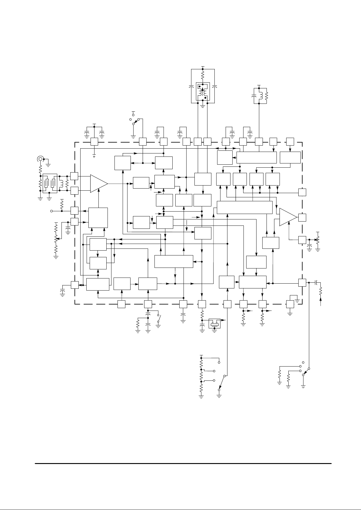
Figure 13. AM Sound IF Frequency Response Figure 14. AM Sound Detector Frequency Response
Figure 15. AM Sound Detector Linearity Figure 16. Variable Audio Output Frequency Response
0
–4.0
–8.0
–12
–16
–20
–24
–28
0
–2.0
–4.0
–6.0
–8.0
–10
–12
–14
0
–4.0
–8.0
–12
–16
–20
–24
–28
2.5
2.0
1.5
1.0
0.5
1.0 10 100 100020 50 200
1.0 10 100 1000 1000020 40 60 80 100 120 140 160
VCC = 5.0 V
NTSC Mode Selected
fC = 4.5 MHz
TA = 25
°
C
5.0 10
VCC = 5.0 V
SECAM Mode Selected
Vin = 60 mVrms into Pin 23
Mod = 30% AM, 1.0 kHz
RL = 10 M
Ω
CL = 10 pF
TA = 25
°
C
VCC = 5.0 V
SECAM Mode Selected
Vin = 60 mVrms into Pin 23
Mod = 30% AM
RL = 10 M
Ω
CL = 10 pF
TA = 25
°
C
VCC = 5.0 V
Vin = 200 mVrms into Pin 3
Pin 3 = 22 k to Gnd
RL = 10 M
Ω
CL = 10 pF
TA = 25
°
C
100
0
160
0
20
I
CC
, SUPPLY CURRENT (mA)
VCC, SUPPLY VOLTAGE (V)
VARIABLE AUDIO OUTPUT GAIN (dB)
Figure 17. Variable Audio Output Gain
versus Volume Control Voltage
VOLUME CONTROL VOLTAGE (V)
Figure 18. Supply Current Versus Supply Voltage
0
–20
–40
–60
–80
120
80
40
0
1.0 2.0 3.0 4.01.0 2.0 3.0 4.0 5.0 5.0 6.0 7.0
Minimum
Operating
Voltage
Range
VCC = 5.0 V
Audio 2 Selected, Pin 3 = 22 k to Gnd
Vin = 200 mVrms into Pin 3
f = 1.0 kHz
TA = 25
°
C
Vin = 1.0 mVrms
fC = 45.75 MHz
TA = 25
°
C
Pin 25 supply current measured in Figure 28 circuit
with 87.5% modulated grayscale in NTSC Mode.
MC44302A
8
MOTOROLA ANALOG IC DEVICE DATA
Figure 19. Representative Block Diagram
This device contains 2,641 active transistors.
V
CC
8
9
14
17 16 18 28
10
13
1225 11
15
1
27
24
232267419 2120
2256
Sound
AFT Filter/
Peak
White Filter
Sound
De–
Emphasis
(FM)
AM IF &
Detector
FM IF & Detector
Switch
4
Switch
3
Switch
2
Switch
1
VCO
FM
AFT
V
CC
V
CC
V
CC
V
CC
V
CC
V
CC
V
CC
Gnd
(Pos)(Neg)
Video
Mode
Switch
From
External
Audio
Source
Audio 1
Audio 2
Video 1 Video 2
NTSC
SECAM
PAL 2
PAL 1
Intercarrier
Sound Output
Lock Detector/
Filter
(Acquisition Circuit)
Horizontal PLL Filter
Flyback/
Video Input
Video Invert
Switch
Mode
Switch
Phase
Detector
AFT
Amp
AFT
Clamp
AFT
Switch
Limiter
AGC
Control
Circuit
Limiter
VCO
Sweep
Freq
Doubler
Control
Logic
Audio
Switch
White
Spot Inv
Sound
Q Det
Video 1
Det
Phase
Shift 90
°
Acquisition
Circuit
Horiz PLL
OSC
Sync
Sep
AGC
Discharge
Peak
AGC
Gated
AGC
AFT
Output
PLL Filter
(Main VCO Loop)
IF Input
RF AGC
Output
RF
AGC
Delay
AGC
Filter
Volume
Control
Audio Output
(Variable)
Audio Output
(Constant)
Audio Input/
Audio–Video
Switch
Sound Inputs
(AM)(FM)
Sound
Quadrature
Coil (FM)
VCO
Coil
3
90
°
IF
Amp
Vol
Control
Video Outputs
0
°
90
°

MC44302A
9
MOTOROLA ANALOG IC DEVICE DATA
FUNCTIONAL DESCRIPTION
Introduction
The MC44302A is an advanced high performance
multistandard IF system specifically designed for use with all
of the world’s major television modulation techniques
including NTSC, PAL, and SECAM. This device performs the
function of intermediate frequency (IF) amplification,
automatic gain control (AGC), automatic frequency tuning
(AFT) and signal demodulation for transmitting systems that
use either positive or negative amplitude modulated video
along with frequency modulated (FM) or amplitude
modulated (AM) sound. The television designer is offered a
new level of circuit simplicity along with enhanced system
performance when compared to present day television IF
amplifiers. Numerous unique design techniques are
incorporated resulting in only a single tuned circuit
adjustment for a completely aligned video and sound IF
system with tuner AFT output. Special design attention was
given to enhance noise performance and to reduce
differential gain and phase distortion. Additional internal
circuitry is provided to meet the European Peritel socket
requirements along with a means for descrambling video
signals that use either or both amplitude modulated sync and
alternate line video inversion. A detailed block diagram of the
internal architecture is shown in Figure 19 and an operating
description of the major circuit blocks is given below.
IF Amplifier and AGC
The IF amplifier consists of four cascaded ac coupled gain
stages yielding an input sensitivity of 40 µV for a full video
output swing of 2.2 Vpp. This level of sensitivity allows the
use of a single IF block filter without incurring the additional
cost of a preamplifier. A quite acceptable level of signal to
noise performance is achievable by utilizing a tuner with a
gain of 33 dB to 36 dB combined with a low insertion loss
(≤18 dB) surface acoustic wave (SAW) or passive block filter.
The first three stages of the IF amplifier are gain controlled to
provide an AGC range of 80 dB. This extended AGC range
enhances the signal handling capability, resulting in superior
differential phase and gain performance with a significant
reduction of intermodulation products. AGC of the first stage
is internally delayed so as to preserve the amplifier’s low
noise figure characteristics.
An on–chip sync separator and horizontal phase–locked
loop oscillator is provided for noise immune AGC gating in
self contained applications where a horizontal scan signal
may not be available. A positive going sync source connected
to the Flyback/Video input at Pin 17 is used to lock the PLL
and generate an internal AGC keying pulse. The sync
separator allows direct use of the Negative Video output at
Pin 5 as a source for the keying pulse. If horizontal scan
circuitry is available, a positive going flyback pulse can also
be used to set the keying pulse.
A video signal and a reference level are required to
implement automatic gain control of the lF and tuner. The
video AGC reference is selected for a specific modulation
standard by the Video Mode Switch voltage setting at Pin 10;
refer to Table 2. With PAL 1, PAL 2, or NTSC mode selected,
a black level reference is established by AGC keying during
the tip of sync. With SECAM mode selected, a black level
reference is established by AGC keying during the back
porch. In order to correct for the inconsistent back porch level
that is common between SECAM transmitters, a long time
constant non–keyed peak white reference level is also
established, and is used in conjunction with the black level
reference to control the video output level. The peak white
level is used in effect to slowly readjust the black level
reference threshold over a limited range of ±10%. With this
dual reference approach, the accuracy associated with a
typical peak white detecting system is maintained without the
usual sacrifice of speed, thus allowing a quick AGC response
to airplane flutter and channel changes.
The tuner AGC control function consists of an RF AGC
delay adjustment at Pin 15 and an RF AGC output at Pin 13.
The delay adjustment sets the threshold where tuner gain
reduction is to begin. This usually corresponds to a signal
level of 1.0 mV to 2.0 mV at antenna input. The AGC output
is designed to control a reverse AGC type of tuner. As the
antenna signal level increases, the voltage at Pin 13
decreases, causing a gain reduction in the tuner. Since
Pin 13 is an NPN open collector output, an external pull–up
resistor must be added if one is not provided in the tuner.
Pin 13 is guaranteed to sink a minimum of 1.0 mA. Note that
when operating with a tuner that requires in excess of 5.6 V,
current will flow into Pin 13 due to conduction of the upper
internal clamp diode.
Carrier Regeneration
Carrier regeneration is attained by the use of a
phase–locked loop, thus enabling true synchronous
demodulation to be achieved with all of its advantages.
Following the IF amplifier and preceding the PLL phase
detector is a limiting amplifier designed to remove the
amplitude modulation that is present on the carrier. The
amplifier consists of two cascaded differential stages with
direct coupled feedback to set a closed loop gain of 40 dB.
This two stage approach has several distinct advantages
when compared to conventional integrated demodulators
that utilize a single stage limiter. With a two stage limiter, the
gain requirement to remove the video amplitude modulation
can be designed–in without the large voltage swings that are
required by a single stage limiter with equivalent gain. The
large voltage swings lead to poor differential phase and gain
performance, and consequently the need for an external
tuned circuit with two cross coupled limiting diodes. Use of
direct coupled feedback diminishes the effects of the
amplifier’s input offset voltage which can be an additional
source for differential phase and gain errors. The
combination of low voltage swing per stage with dc feedback
eliminates the need for a tuned circuit at the output of the
limiter. This results in a significant component and alignment
cost savings as well as removing the necessity to pin out a
high level IF signal. This high level signal is a potential
radiation source that can result in IF instability at low signal
levels. The only problem of using the two stage limiter is the
potential for an additional static phase shift which will result in
a change of the demodulating angles at both the video and
sound demodulators inputs. This problem is solved by
placing an identical two stage limiter between the frequency
doubler output and the phase detector input. This adds an
identical amount of static phase shift to bring the
demodulating angles back to 0° and 90°.
 Loading...