MC44251MOTOROLA
1
Advance Information
CMOS
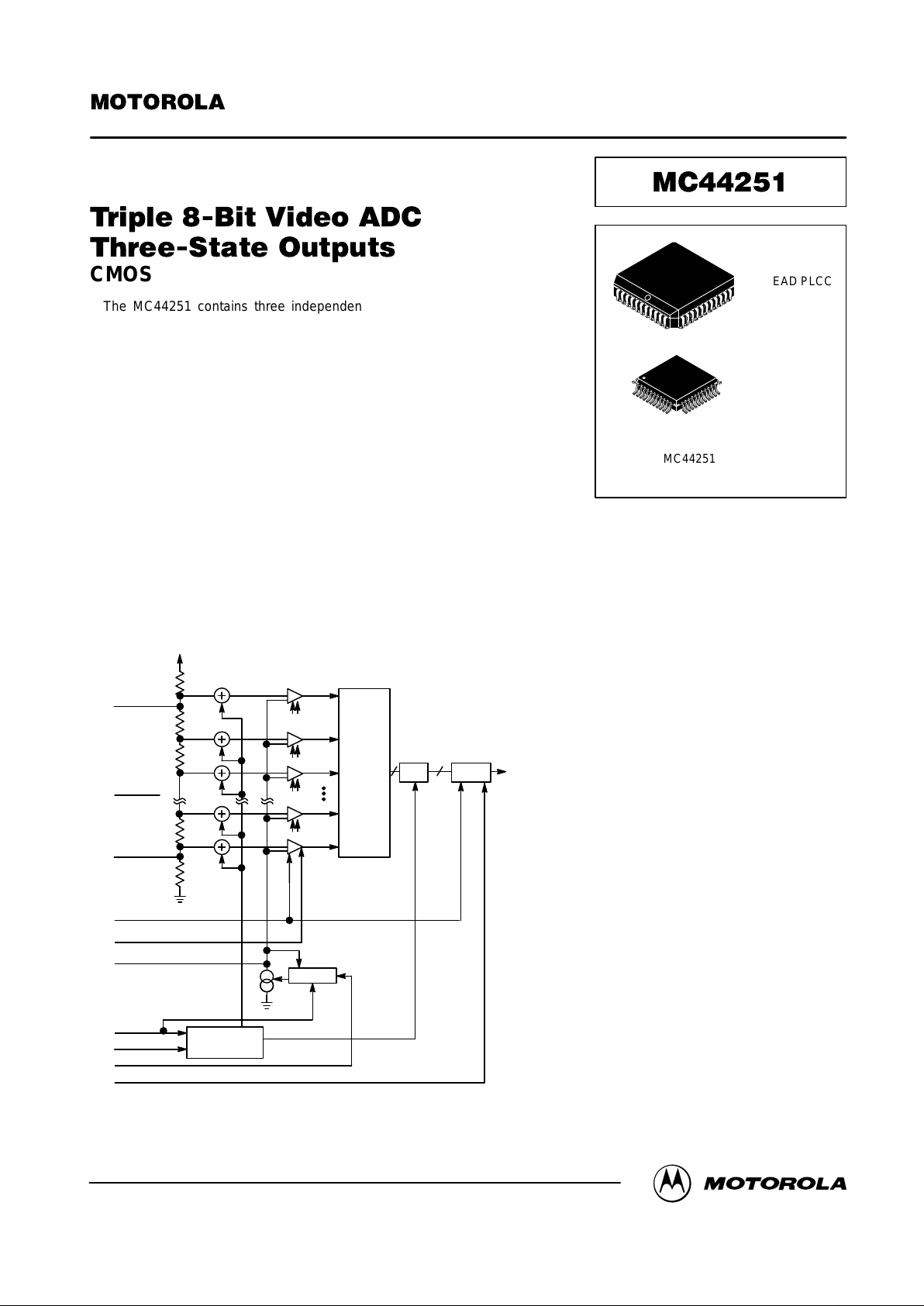
The MC44251 contains three independent parallel analog–to–digital flash
converters (ADC). Each ADC consists of 256 latching comparators and an
encoder. Video may be ac or dc coupled. With ac coupling, input clamping
provides for internal dc restoration. The MC44251 also contains a dithering
generator for video processing performance enhancements.
The MC44251 is especially suitable as a front–end converter in TV–picture
digital processing (picture–in–picture, frame storage, etc.). The high speed
conversion rate of the ADC is suitable for video bandwidth of well over 6 MHz.
• 18 MHz Maximum Sampling Rate
• Three–State Output Buffers
• Output Latching Minimizes Skew
• Input Clamps Suitable for RGB and YUV Applications
• Built–In Dither Generator with Subsequent Digital Correction
• Single 5–Volt Power Supply
• Operating Temperature Range: – 40 to + 85°C
• VTN and HZ Input Threshold Hysteresis Built–In
CLAMP
R
TOP
R
MID
R
BOT
ANALOG INPUT
HZ
MODE
VTN
I
bias
88
Σ
8
DATA
OUTPUTS
V
DD(R)
CS
DITHERING
GENERATOR
LATCH
SIMPLIFIED BLOCK DIAGRAM OF ONE OF THE ADCs
CLOCK
ENCODER
This document contains information on a new product. Specifications and information herein are subject to change without notice.
Order this document
by MC44251/D
SEMICONDUCTOR TECHNICAL DATA
FN SUFFIX
44–LEAD PLCC
CASE 777
ORDERING INFORMATION
MC44251FN PLCC
MC44251FU QFP
44
1
44
1
FU SUFFIX
44–LEAD QFP
CASE 824A
NOTE:
The FN package is not
recommended for new designs.
It is scheduled for phase out
in late 1996.
Motorola, Inc. 1996
REV 4
7/96
MC44251 MOTOROLA
2
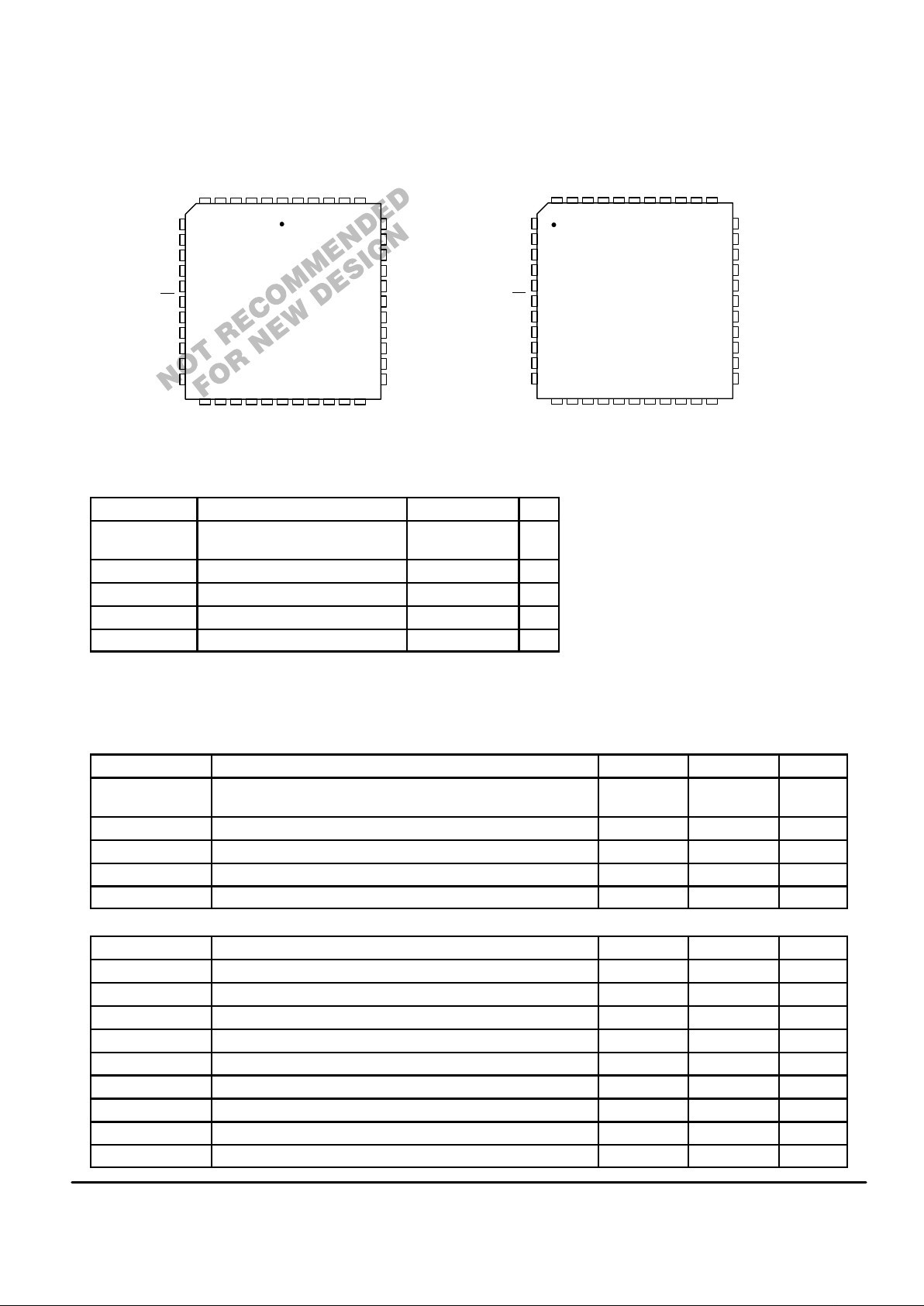
PIN ASSIGNMENTS
7
8
9
10
11
12
13
14
15
16
17
39
38
37
36
35
34
33
32
31
30
29
1819202122232425262728
65432
1
4443424140
B7
G0
G1
G2
G3
CS
G4
G5
G6
G7
R0
VB6B5B4VB3B2B1B0
MODE
V
V
R7
R5
CLOCK
R4
V
R3
R2
R1
I
bias
V
SS(R)
B
in
R
BOT
G
in
R
MID
R
in
R
TOP
V
DD(R)
VTN
HZ
DD(D)
SS(D)
DD(A)
R6
DD(D)
SS(D)
V
SS(A)
QFP
1
2
3
4
5
6
7
8
9
10
11
33
32
31
30
29
28
27
26
25
24
23
1213141516171819202122
4443424140393837363534
B7
G0
G1
G2
G3
CS
G4
G5
G6
G7
R0
VB6B5B4VB3B2B1B0
MODE
V
V
R7
R5
CLOCK
R4
V
R3
R2
R1
I
bias
V
SS(R)
B
in
R
BOT
G
in
R
MID
R
in
R
TOP
V
DD(R)
VTN
HZ
DD(D)
SS(D)
DD(A)
R6
DD(D)
SS(D)
V
SS(A)
PLCC
ABSOLUTE MAXIMUM RATINGS
Symbol Characteristic Value Unit
V
DD(A)
, V
DD(D)
,
V
DD(R)
DC Supply Voltage (referenced to
VSS)
– 0.5 to + 6.0 V
V
in
Input Voltage, All Pins – 0.5 to VDD + 0.5 V
I
in
DC Input Current per Pin ± 20 mA
I
out
DC Output Current per Pin ± 25 mA
T
stg
Storage Temperature Range – 65 to + 150 °C
NOTE: Maximum Ratings are those values beyond which damage to the device may occur.
Functional operation should be restricted to the Recommended Operating
Conditions.
ELECTRICAL CHARACTERISTICS (Voltages Referenced to V
SS
) (V
DD(R)
= V
DD(A)
= V
DD(D)
; R
bias
(Pin 33) = 5 kΩ to ground)
OPERATING RANGES
Symbol Characteristic Min Max Unit
V
DD(A)
, V
DD(D)
,
V
DD(R)
Power Supply Voltage 4.5 5.5 V
I
DD(A)
Analog Supply Current — 55 mA
I
DD(R)
Reference Supply Current —
28
mA
I
DD(D)
Digital Supply Current — 5 mA
T
A
Operating Ambient Temperature Range – 40 + 85 °C
A/D CONVERTER
Symbol Characteristic Min Max Unit
C
in
Input Capacitance — 60 pF
V
min
See Figure 11 0.3 x V
DD
0.36 x V
DD
V
V
max
See Figure 11 0.89 x V
DD
0.93 x V
DD
V
V
range
See Figure 11 0.57 x V
DD
0.59 x V
DD
V
Gain See Figure 11 (Note 1) 0.95 1.0 LSB
DNL Differential Nonlinearity (Note 1) — ± 1.0 LSB
INL Integral Nonlinearity (Note 1) — ± 2.0 LSB
E
gain
Gain Difference (Note 2) — ± 1.0 %
E
off
Offset Difference (Notes 1, 2) — ± 3.0 LSB
This device contains protection circuitry to
guard against damage due to high static voltages or electric fields. However, precautions
must be taken to avoid applications of any
voltage higher than maximum rated voltages to
this high–impedance circuit. For proper operation, Vin and V
out
should be constrained to the
range VSS ≤ (Vin or V
out
) ≤ VDD.
Unused inputs must always be tied to an
appropriate logic voltage level (e.g., either V
SS
or VDD). Unused outputs must be left open.
MC44251MOTOROLA
3
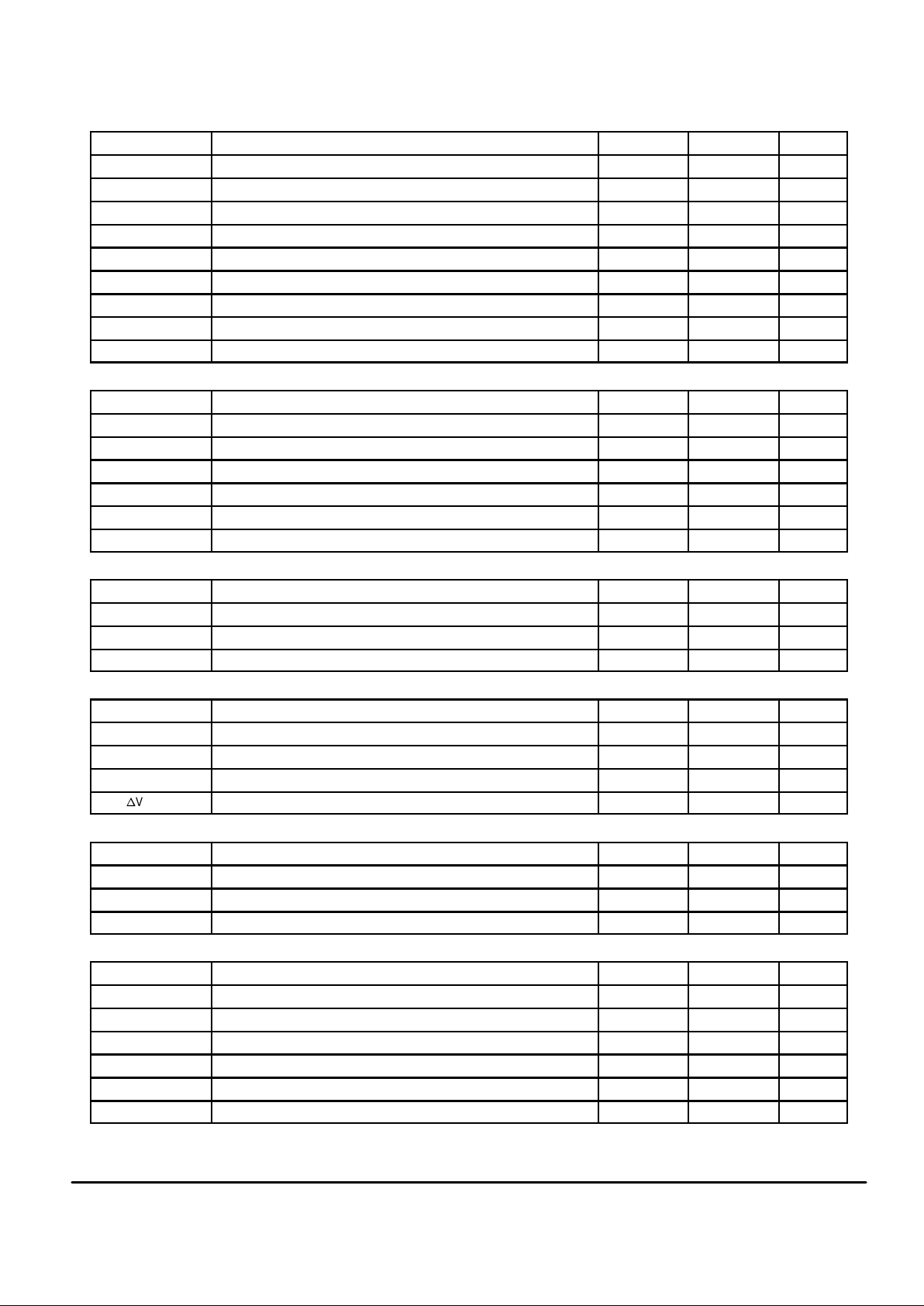
CLOCK INPUT
Symbol Characteristic Min Max Unit
V
IH
Clock Input High Level 4.2 — V
V
IL
Clock Input Low Level — 0.8 V
I
IL
Low Level Input Current — ± 2.0 µA
I
IH
High Level Input Current — ± 2.0 µA
RATE Conversion Rate — 18 ms/s
t
wL
Clock Low Duration, Figure 1 27.5 — ns
t
wH
Clock High Duration, Figure 1 27.5 — ns
t
r
Clock Rise Time (10% to 90%), Figure 1 — 15 ns
t
f
Clock Fall Time (10% to 90%), Figure 1 — 15 ns
HZ AND VTN INPUTS
Symbol Characteristic Min Max Unit
V
IH
HZ and VTN Input Turn–On Threshold Voltage 0.56 x V
DD
— V
V
IL
HZ and VTN Input Turn–Off Threshold Voltage — 0.29 x V
DD
V
V
HYS
Hysteresis Voltage 0.11 x V
DD
0.17 x V
DD
V
I
IL
Low Level Input Current — ± 2.0 µA
I
IH
High Level Input Current — ± 2.0 µA
t
H
HZ High Time, Figure 3 3 — ns
CHIP SELECT INPUT
Symbol Characteristic Min Max Unit
V
IH
Input High Level 3.5 — V
V
IL
Clamping Source Current — 1.5 V
I
IN
Input Leakage Current — ± 2.0 µA
CLAMPING NETWORK (Measured on R,G,B Inputs)
Symbol
Characteristic Min Max Unit
I
sink
Clamping Sink Current 2.0 5.0 µA
I
source
Clamping Source Current – 5.0 – 2.0 µA
D
ICL
Clamping Current Difference (Note 2) — 0.5 µA
n
V
damp
Clamping Levels (Max. Deviation Compared to Table 1) — ± 1.5 LSB
RESISTIVE REFERENCE NETWORK
Symbol Characteristic Min Max Unit
Z
TOP
R
TOP
Output Impedance 28 48 Ω
Z
BOT
R
BOT
Output Impedance 70 130 Ω
Z
MID
R
MID
Output Impedance 70 130 Ω
MODE INPUT
Symbol Characteristic Min Max Unit
V
IL
Logical “0” Level 0 0.8 V
V
IH
Logical “1” Level 4.2 V
DD(D)
V
V
IZ
Logical “Open” Level 2 2.8 V
I
IL
Input Current at “0” Level — ± 50 µA
I
IH
Input Current at “1” Level — ± 80 µA
I
IZ
Input Current at “Open” Level — ± 50 µA
MC44251 MOTOROLA
4
DATA OUTPUTS
Symbol Characteristic Min Max Unit
t
d
Delay from Sample Clock to Valid Output, Figure 2 2.5 2.5 Cycle
I
OL
Output Sinking Current at V
out
= 0.4 V 2.0 — mA
I
OH
Output Sourcing Current at V
out
= VDD – 0.1 V – 0.4 — mA
t
QLH
, t
QHL
Propagation Delay from the Clock Rising Edge to Valid Data Output
(CL = 15 pF), Figure 1
— 40 ns
I
OTR
Maximum Three–State Leakage Current — ± 50 µA
NOTES:
1. Unit “LSB” means ideal LSB (see definitions section).
2. “Difference” means difference between any two converters in the same package.
50%
CLK
V
DD(D)
V
SS(D)
t
f
10%
90%
t
r
t
wH
t
wL
DATA
OUTPUT
50%
t
QLH
, t
QHL
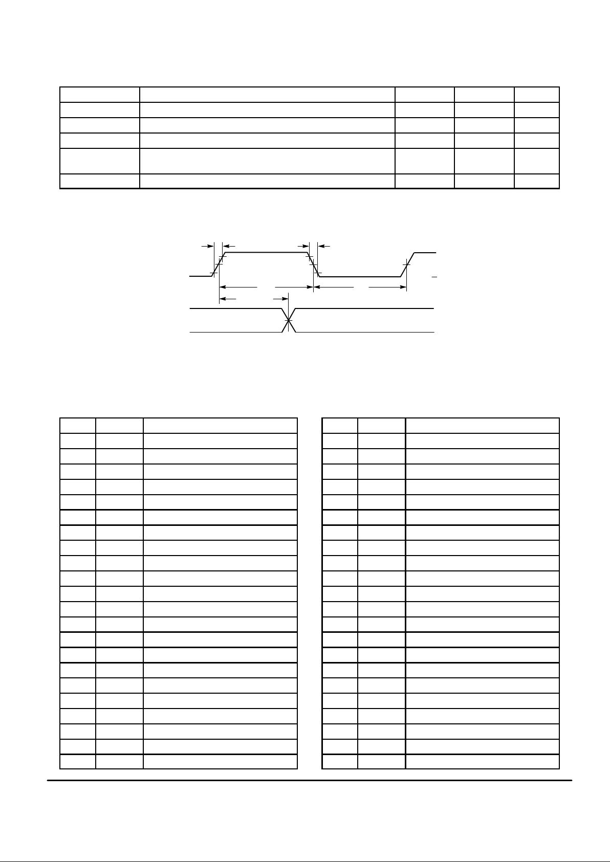
Figure 1. Clock and Output Timing
PIN DESCRIPTIONS
Pin No. Name Function
1 B7 Output Blue, Bit 7 (MSB)
2 G0 Output Green, Bit 0 (LSB)
3 G1 Output Green, Bit 1
4 G2 Output Green, Bit 2
5 G3 Output Green, Bit 3
6 CS Chip Select
7 G4 Output Green, Bit 4
8 G5 Output Green, Bit 5
9 G6 Output Green, Bit 6
10 G7 Output Green, Bit 7 (MSB)
11 R0 Output Red, Bit 0 (LSB)
12 V
DD(D)VDD
, Digital
13 R1 Output Red, Bit 1
14 R2 Output Red, Bit 2
15 R3 Output Red, Bit 3
16 V
SS(D)VSS
, Digital
17 CLK Clock Input
18 R4 Output Red, Bit 4
19 R5 Output Red, Bit 5
20 R6 Output Red, Bit 6
21 R7 Output Red, Bit 7 (MSB)
22 V
SS(A)VSS
, Analog
Pin No. Name Function
23 HZ Horizontal Sync
24 VTN Vertical Sync
25 V
DD(R)VDD,
reference
26 R
TOP
Reference Tapping, Top
27 R
in
Analog Input, Red
28 R
MID
Reference Tapping, Middle
29 G
in
Analog Input, Green
30 R
BOT
Reference Tapping, Bottom
31 B
in
Analog Input, Blue
32 V
SS(R)VSS
for Reference Voltage
33 I
BIAS
To External Bias Resistor
34 V
DD(A)VDD
, Analog
35 MODE Clamp Level Select Input
36 B0 Output Blue, Bit 0 (LSB)
37 B1 Output Blue, Bit 1
38 B2 Output Blue, Bit 2
39 B3 Output Blue, Bit 3
40 V
SS(D)VSS
, Digital
41 B4 Output Blue, Bit 4
42 B5 Output Blue, Bit 5
43 B6 Output Blue, Bit 6
44 V
DD(D)VDD
, Digital

MC44251MOTOROLA
5
RESISTIVE REFERENCE NETWORK
R
TOP
(Pin 26)
R
BOT
(Pin 30)
R
MID
(Pin 28)
Taps on the reference ladder are pinned out, providing
access to the bottom (R
BOT
), the top (R
TOP
), and the middle
scale points. These pins are intended for ac bypassing as
ladder noise may present a problem. The value of the decoupling capacitor should not exceed 47 nF. Large capacitance values can cause problems because of the amount of
energy stored. When a system containing the MC44251 is
rapidly powered down and up, the capacitor voltage may
exceed the supply voltage during the power up and cause a
latch–up condition. Failure to adequately decouple these
pins can adversely affect the conversion process.
SUPPLY PINS
V
DD(A)
(Pin 34)
V
DD(D)
(Pins 44, 12)
V
DD(R)
(Pin 25)
The three types of supply pins are analog, digital, and
reference. The dc voltage applied to all four pins must be
maintained such that
V
DD(A)
= V
DD(D)
= V
DD(R)
.
Each pin must be carefully decoupled to ground as close
to the package as possible, and particular care should be
taken with V
DD(R)
as any noise present on this pin will
appear in the output data as an equivalent input noise. This
noise will be present on the Rin, Gin, and Bin input pins in a
ratio of 1:1 to the input noise (worst case condition). Noise
reduction can be improved by incorporating choke coil inductors in series with the power supply rails.
ANALOG INPUTS
Rin (Pin 27)
Gin (Pin 29)
Bin (Pin 31)
The analog signals to be converted are input at these pins.
An on–chip clamp circuit for dc restoration is available when
using ac coupling. The clamp circuit operation is activated by
the presence of the signal at the HZ input. This signal is
derived from the composite sync information and must be
coincident with the horizontal sync of the composite video
waveform for proper operation. Yin, Uin, and Vin may be used
instead of the RGB signals. In this case the conversion will
be a YUV analog–to–digital conversion.
I
bias
(Pin 33)
The comparator bias current is set by connecting an exter-
nal resistor between I
bias
and ground. The conversion rate is
guaranteed for a resistor value of 5.1 kΩ ± 5% and will
decrease logarithmically with increased resistance. The
resistor must be placed adjacent to the I
bias
pin. No decoup-
ling capacitor is allowed on this pin.
DIGITAL OUTPUTS
R0 – R7 (Pins 11, 13 – 15, 18 – 21)
G0 – G7 (Pins 2 – 5, 7 – 10)
B0 – B7 (Pins 36 – 39, 41 – 43, 1)
These pins are the parallel output for the digital value for
the RGB signals. R0 through R7 are the digital equivalent of
the analog RED input, G0 through G7 are equivalent to the
GREEN input, and B0 through B7 are equivalent to the BLUE
input. If YUV analog signals have been input instead of the
RGB signals; the digital outputs will be Y0 through Y7, U0
through U7, and V0 through V7.
DIGITAL INPUTS
Clock (Pin 17)
The analog input voltages to be converted are sensed at
the falling edge of the clock signal and the corresponding
data is present on the digital outputs at the clock signal rising
edge, 2.5 cycles later (see Figure 2).
HZ (Pin 23)
This is the horizontal synchronization input, and is used to
increment the dither generator. The clamp network is also
controlled by HZ to ensure proper dc restoration for Rin, Gin,
and Bin before conversion. Schmitt trigger input is included to
improve noise immunity.
VTN (Pin 24)
The vertical synchronization input, VTN, resets the dither
generator after every second vertical sync pulse (after each
frame). Schmitt trigger input is included to improve noise
immunity.
MODE (Pin 35)
This pin is used to select the proper clamp levels (see
Table 1).
CHIP SELECT (Pin 6)
Chip select is an active low input used to enable the ADC
for data transfers. When the CS
is at a high level, the digital
output is forced to a high impedance state.
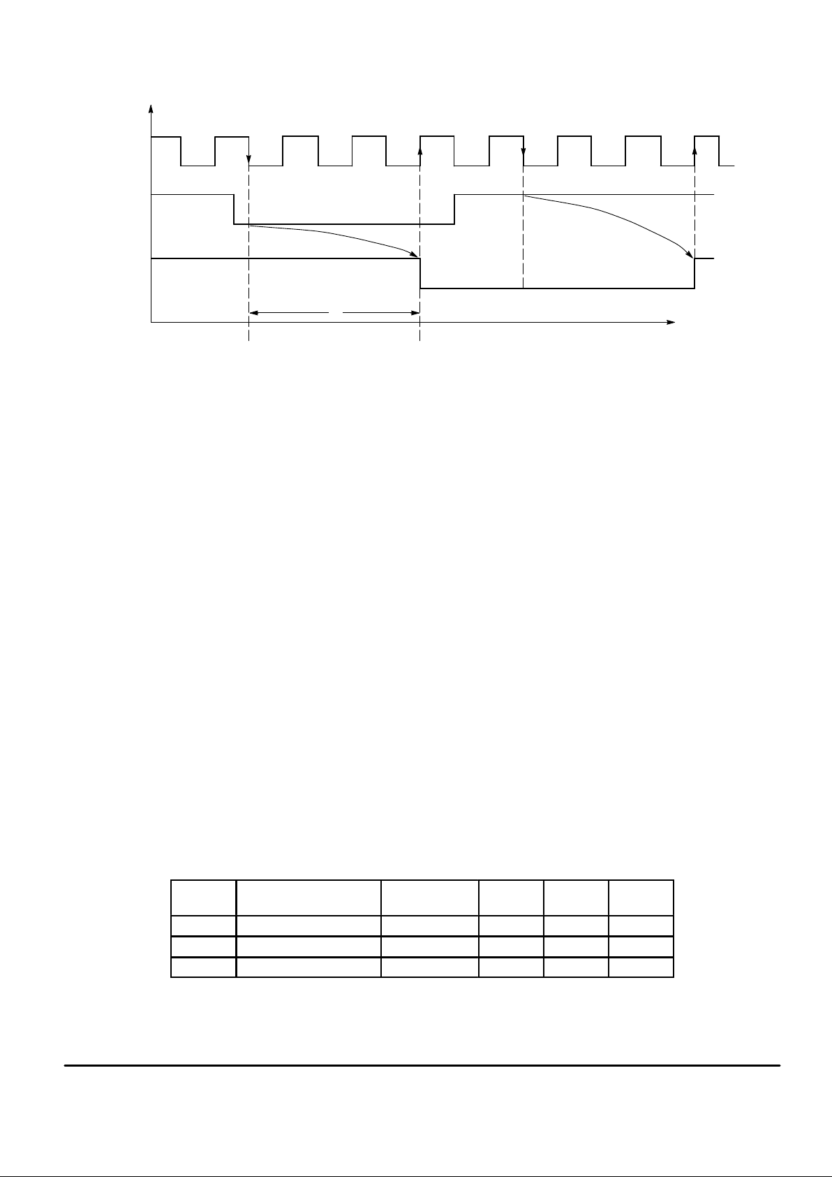
MC44251 MOTOROLA
6
t
d
CLK
IN
OUT
Figure 2. Conversion Timing Functional Characteristics
CIRCUIT OPERA TION
GENERAL
The MC44251 contains three independent parallel analog–to–digital converters (ADC). Each ADC consists of 256
latching comparators and an encoder. The MC44251 may be
used to convert RGB or YUV video information from an analog to a digital format, or as a triple ADC for non–video information. For video processing performance enhancement,
each ADC has a dither generator with subsequent digital
correction designed into it. The dithering generator reduces
display degradation from granulation of the luminance
information caused by quantization errors of the digitizing
process. Each ADC is driven from a common clock and
receives common sync information from the HZ and VTN
pins. In addition, the VTN pin controls the dithering function
and disables the dithering generator when VTN is pulled low.
The sampling of the analog input signals occurs at the falling
edge of the clock signal, whereas the digital outputs change
state at the rising clock edge. The bias current of the
comparators is set by an external resistor. Input clamps allow
for ac coupling of the input signals.
CLAMP NETWORK
The MC44251 can be operated either dc coupled or ac
coupled. When dc coupled, the MC44251 will track the average dc level of the input waveform. For ac coupling, an
on–chip dc restoration circuit samples and adjusts the average dc level of the input signal. The MC44251 has three
selectable clamping levels for ac coupling. The clamp levels
are selected by the MODE pin according to Table 1. In the
RGB mode, the clamping levels are set to 16/256, corresponding to 6.3% of full range. In the YUV mode, the UV
clamping levels are set to 128/256 (50%) and the Y input to
either 16/256 or 64/256 (25%).
When input HZ (horizontal) is high, as illustrated in Figure 3a, the voltage difference between the analog input voltage and the clamp reference voltage is integrated within
each clamp network. At the falling edge of HZ, a latching
comparator senses the sign of the integrator output voltage.
Depending on this result, either a sinking or a sourcing current is applied to the analog input pin as long as input HZ remains low.
For video applications, the timing of HZ is critical to the
proper operation of the ADC. The frequency of HZ should be
locked to the line frequency of the video input. The pulse
width and timing of HZ with respect to the video signal is
shown in Figure 4. The top curve represents the horizontal
synchronizing and blanking interval for a video signal. The
pulse width of HZ (t
H
) should be less than the width of the
back porch (tBP) and coincident with it. In all cases, HZ must
return low before the end of the back porch (tBP).
Table 1. Clamping Levels
MODE
(Pin 35)
Application Clamp Levels G
in
R
in
B
in
L RGB 16/256 16/256 16/256
H YUV Mode Without Sync Format 16/256 128/256 128/256
Open YUV Mode With Sync 64/256 128/256 128/256
 Loading...