Motorola MC44145D Datasheet

Order this document by MC44145/D
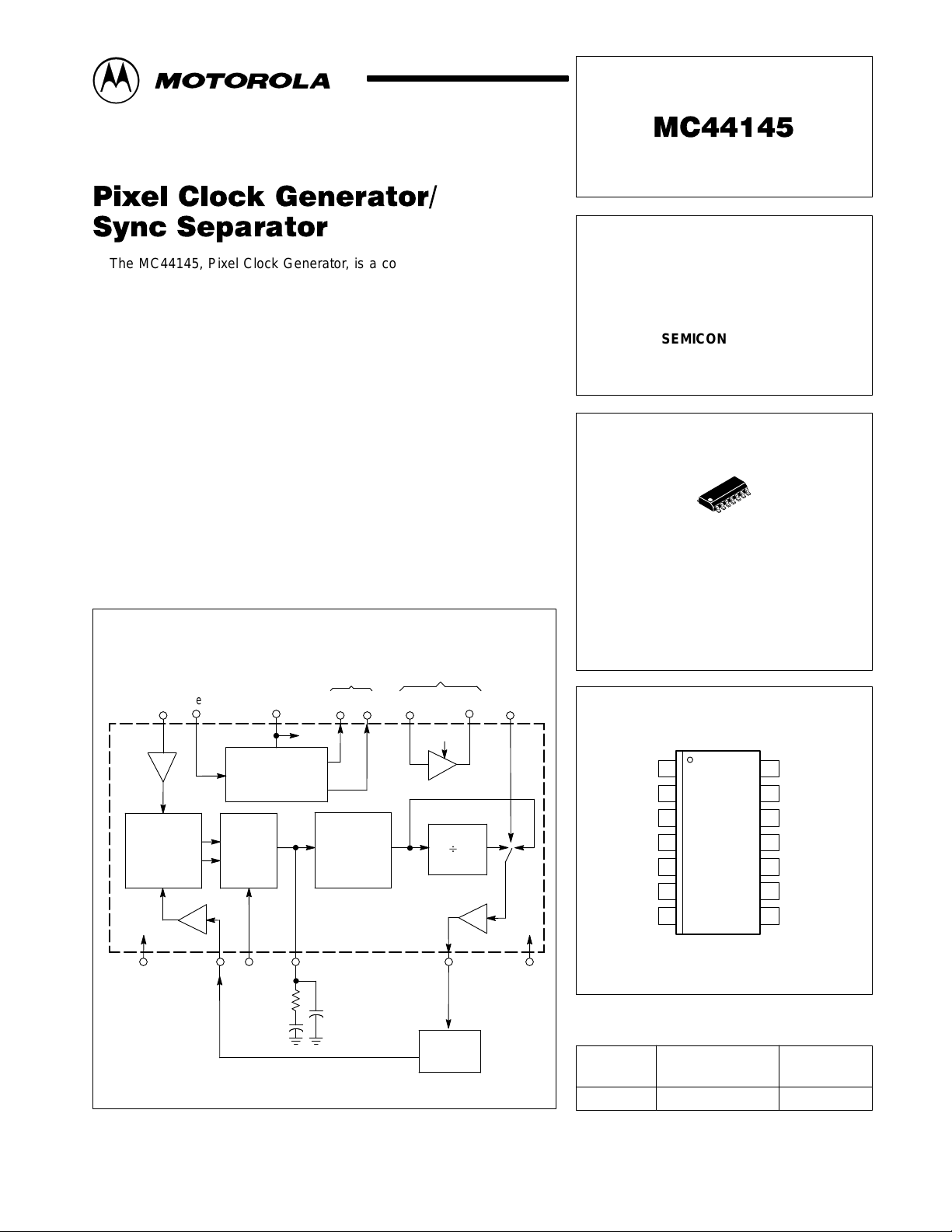
The MC44145, Pixel Clock Generator, is a component of the MC44000
family.
The MC44145 contains a sync separator with composite sync and vertical
outputs, and clock generation circuitry for the digitization of any video signal
along with the necessary circuitry for clock generation, such as a phase
comparator and a divide–by–2 to provide a 50% duty cycle.
The MC44145 is available in a SO–14 package and is fabricated in the
Motorola high density, high speed, low voltage, process called MOSAIC 1.5.
MOSAIC is a trademark of Motorola, Inc.
Representative Block Diagram
V
CC
Video InF
ref
12 11953 4 10 8
Sync Sep
Sync Out Sync Amp
A
InCB
A
Out
Div 2
EN
PIXEL CLOCK GENERATOR/
SYNC SEPARATOR
SEMICONDUCTOR
TECHNICAL DATA
14
1
D SUFFIX
PLASTIC PACKAGE
CASE 751A
(SO–14)
PIN CONNECTIONS
Sync
Separator
Phase and
Frequency
Comparator
613114 7 2
V
CC
Up
Charge
Pump
Dn
NBACK NPD
Gain
This device contains 214 active transistors.
V
C
VCO
MC44145
PLL Loop
Filter
R
C
C2
B
2
Clock Out Gnd
External
Divider
2F
F
O
O
MOTOROLA ANALOG IC DEVICE DATA
NPD Gain
Gnd
Sync B
Sync Amp In
Sync C
V
CC
Clock Out
1
2
3
4
5
6
7
(Top View)
PLL Loop Filter
14
NBACK
13
Video In
12
V
11
CC2
Sync Amp Out
10
F
9
ref
Div 2 EN
8
ORDERING INFORMATION
Operating
Device
MC44145D TA = 0° to +70°C SO–14
Motorola, Inc. 1996 Rev 0
Temperature Range
Package
1

MC44145
MAXIMUM RATINGS
Rating Symbol Value Unit
Supply Voltage V
Storage Temperature Range T
Operating Junction Temperature T
NOTE: ESD data available upon request.
V
CC
CC2
stg
J
RECOMMENDED OPERATING CONDITIONS
Characteristic Symbol Pin Min Typ Max Unit
Supply Voltage V
Video Input Amplitude (Note 2) V
NBACK Pulse Width NBACK 13 100 500 – ns
F
Pulse Width F
ref
Operating Ambient Temperature T
V
CC
CC2
in
ref
A
6
11
12 0.4 1.0 2.5 Vpp
9 100 500 – ns
– 0 – +70 °C
ELECTRICAL CHARACTERISTICS
Characteristic Symbol Note Pin Min Typ Max Unit
POWER SUPPLY
Supply Current (Note 1) I
Supply Current I
SYNC SEPARATOR (VCC = 5.0 V; TA = 25°C, unless otherwise specified.)
Sync B Output – 3 3 – 5.0 to 0 – V
Sync C Output (1.0 mA Source) – 4 5 – 0 to 3.3 – V
Slicing Level (SL) – – 12 – V
Video Input Sink Current – V
Video Input Source Current – V
NOTES: 1.Operating current for Pin 6 is dependent on the clock frequency (Pin 7). Values given are specified for Pin 14 = 4.0 V.
2.Positive Video.
3.High impedance output.
4.Low impedance output.
CC
CC2
Pin 12
Pin 12
6.0
6.0
–65 to +150 °C
+150 °C
4.75
4.75
– 6 – 15.5 – mA
– 11 – 300 – µA
< S
L
> S
L
V
5.0
5.0
12 – 18 – µA
12 – 1.2 – µA
5.5
5.5
Vdc
CC/2
– V
2
MOTOROLA ANALOG IC DEVICE DATA

MC44145
ELECTRICAL CHARACTERISTICS (continued)
Characteristic
SYNC SEPARATOR (VCC = 5.0 V; TA = 25°C, unless otherwise specified.)
VCO (VCC = 5.0 V; TA = 25°C, unless otherwise specified, divider disabled.)
F
min
F
max
Control Range 2 14 1.0 – 4.0 V
Transfer Function 1 7, 8, 14 – 14 – MHz/V
Input Resistance 9 14 0.5 – – MΩ
Charge Pump 6
Phase Jitter 8 7, 9 – – 3.0 ns
INPUT BUFFERS (F
AND NBACK) (TA = 25°C, unless otherwise specified.)
ref
Threshold (TTL Compatible) – 9, 13 – 2.5 – V
Input Current – 9, 13 – – 1.0 µA
OUTPUT BUFFER CLOCK (TA = 25°C, unless otherwise specified.)
Sync Amplifier Output High Level 1.0 mA
Sync Amplifier Output Low Level 1.0 mA Sink 10 – 0.2 0.4 V
Rise Time 11 10 – – 6.0 ns
Fall Time 11 10 – – 6.0 ns
Load Capacitance 10 10 – 15 – pF
NOTES: 1.Internal divider disabled.
2.0 V stops the oscillator.
3.Divider ÷2 active.
4.VC = 4.0 V.
5.VC = 1.0 V.
6.PFD gain low.
7.PFD gain high.
8.VCO alone.
9.VC = 4.0 V, charge pumps off.
10. 2 LSTTL loads.
11. With cap load 15 pF and between 10 and 90% of 0.4 and 2.4 V.
Note Pin Min Typ Max Unit
1, 5 7, 8, 14 – – 10 MHz
1, 4 7, 8, 14 39 42 – MHz
7
–
1, 14 –
40
80
–
–
10 2.4 3.0 – V
Source
µA
MOTOROLA ANALOG IC DEVICE DATA
3
 Loading...