Motorola MC44011FN Datasheet
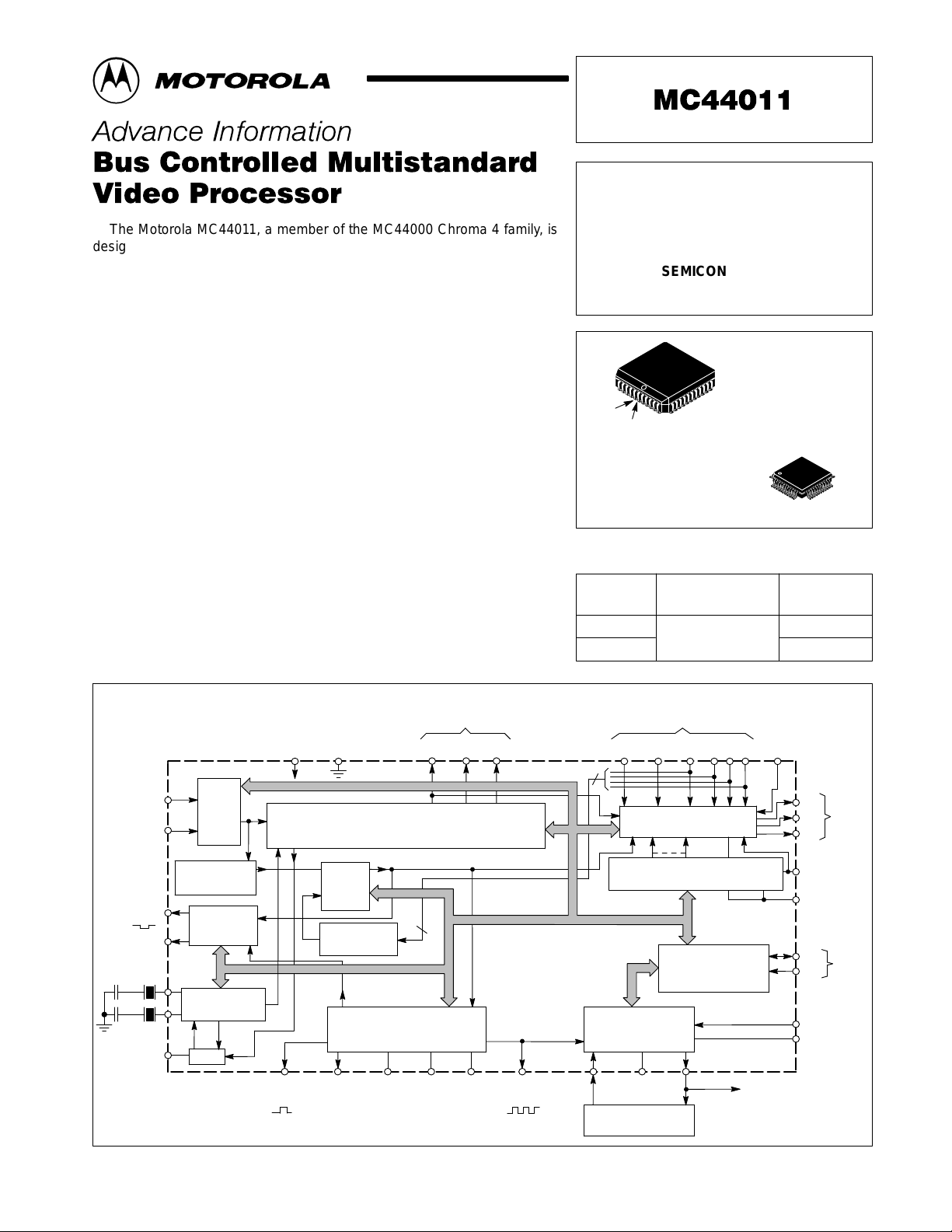
The Motorola MC44011, a member of the MC44000 Chroma 4 family, is
designed to provide RGB or YUV outputs from a variety of inputs. The inputs
can be composite video (two inputs), S–VHS, RGB, and color difference
(R–Y, B–Y). The composite video can be PAL and/or NTSC as the MC44011
is capable of decoding both systems. Additionally , R–Y and B–Y outputs and
inputs are provided for use with a delay line where needed. Sync separators
are provided at all video inputs.
In addition, the MC44011 provides a sampling clock output for use by a
subsequent triple A/D converter system which digitizes the RGB/YUV
outputs. The sampling clock (6.0 to 40 MHz) is phase–locked to the
horizontal frequency.
Additional outputs include composite sync, vertical sync, field
identification, luma, burst gate, and horizontal frequency.
Control of the MC4401 1, and reading of status flags, is via an I2C bus.
• Accepts NTSC and PAL Composite Video, S–VHS, RGB, and R–Y, B–Y
• Includes Luma and Chroma Filters, Luma Delay Lines, and Sound Traps
• Digitally Controlled via I
• R–Y, B–Y Inputs for Alternate Signal Source
• Line–Locked Sampling Clock for A/D Converters
• Burst Gate, Composite Sync, Vertical Sync and Field Identification Outputs
• RGB/YUV Outputs can Provide 3.0 Vpp for A/D Inputs
• Overlay Capability
• Single Power Supply: 5.0 V, ±5%, 550 mW (Typical)
• 44 Pin PLCC and QFP Packages
2
C Bus
BUS CONTROLLED
MULTISTANDARD
VIDEO PROCESSOR
44
1
FB SUFFIX
PLASTIC PACKAGE
CASE 824E
ORDERING INFORMATION
Device
MC44011FN
MC44011FB
Order this document by MC44011/D
SEMICONDUCTOR
TECHNICAL DATA
FN SUFFIX
PLASTIC PACKAGE
CASE 777
(PLCC)
44
(QFP)
Operating
Temperature Range
TA = 0° to +70°C
1
Package
PLCC–44
QFP
Comp
Video 1
Comp
Video 2
Vertical
Output
Field ID
17.7 MHz
14.3 MHz
Filter
Input
Select
Sync
Separator
Vertical
Decoder
Oscillator
PLL
CC1
Burst
Gate
Representative Block Diagram
Outputs
Gnd1V
Sound Trap/Luma Filter/Luma Delay/
Chroma Filter/P AL and NTSC
Decoder/Hue and Saturation Control
Select
Sync
Separator
16Fh/
C
Sync
PLL #1 Horizontal
Filter
Switch
4
PLL/VCO
H
Filter
B–YR–YY1
Quiet
Gnd
MC44011
Fh
Ref
4
15 k
Ret
R–Y
Data Bus
PLL #2
Pixel Clock
PLL/VCO
Frequency
Divider
Inputs
Y2
B–Y
Color Difference
Stage
Contrast, Brightness,
Saturation Control DACs
Interface/
Registers
PLL
Filter
G
R
I2C Data
Clock
B
Fast
Comm
R/V
G/Y
B/U
V
CC2
Gnd2
SDL
SCL
V
CC3
Gnd3
To A/D Converters
Outputs
µ
P
To
This document contains information on a new product. Specifications and information herein
are subject to change without notice.
MOTOROLA ANALOG IC DEVICE DATA
Motorola, Inc. 1996 Rev 1
1
MC44011
Inputs
Outputs
R/V
5.0
5.0
20
Color Matrix and
Blank
Burst
Clamp Clamp Clamp
Gate
CC2
V
(5.0 V)
23
ClampClampClamp
Signal Selection
B–YY R–Y B G R
Gnd2
24
25282726293031424133324334
Sep
T o Sync
G/Y
5.0
21
Controls
B/U
22
Contrast
Saturation
Red Gain
Blue Gain
Brightness
∆
∆
DACs
Color Difference Stage
Red DC
Blue DC
∆
∆
2Fo
Bus Control & Flag Status Read
Voltage
Monitor
SCL
5
C Data
2
Interface/
I
Fo
2
÷
VCO
12–40 MHz
Pump
Charge
U
D
P
µ
To
SDL
6
Registers
T o A/D Converters
Clock
PLL #2
Filter
Ret
15 k
Divider
Frequency
R–Y
B–Y
Hue DACs
C
Saturation/
Outputs
Fs Notch
X1, X2, X8
Delay
Adj. Luma
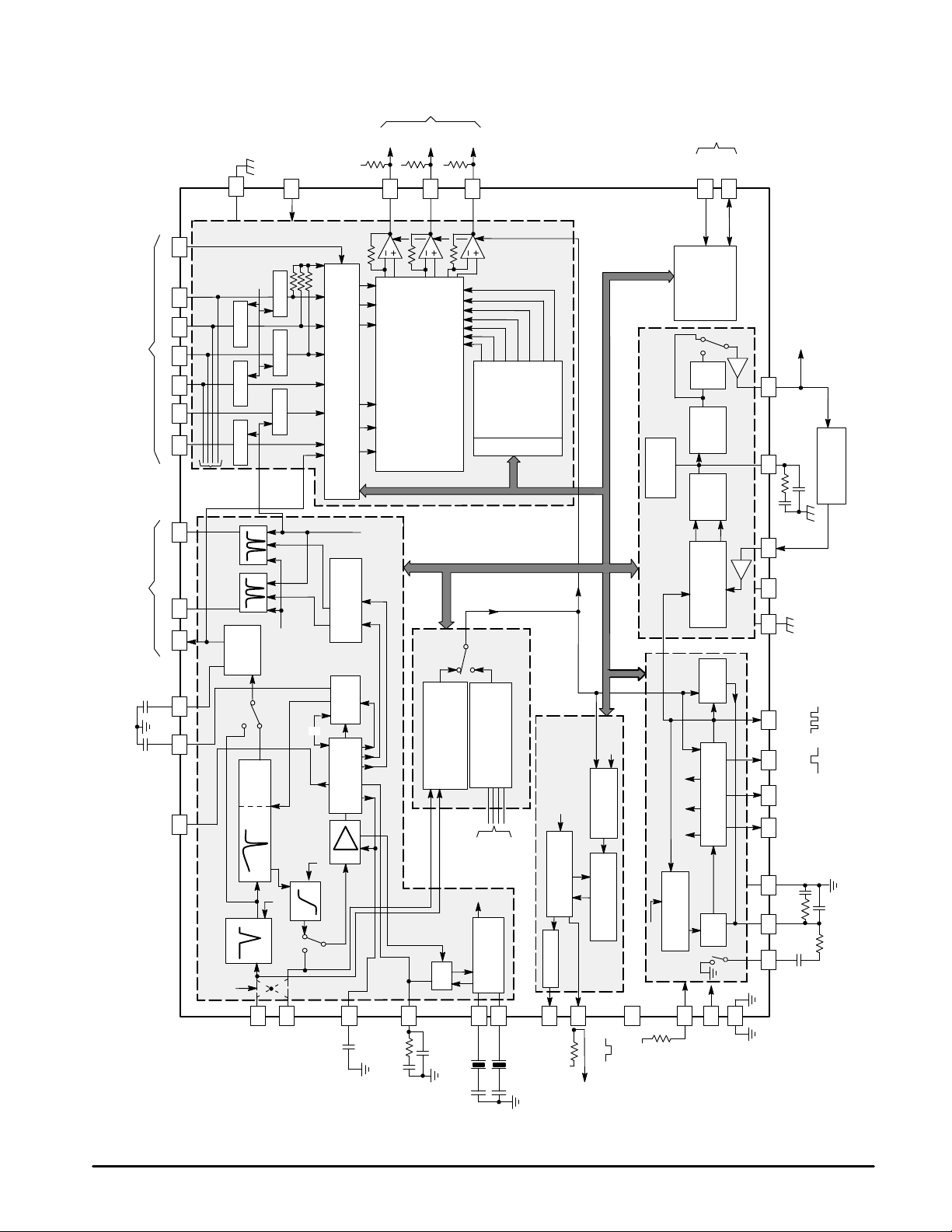
Figure 1. Representative Block Diagram
Y1
Clamp Y1 B–Y R–Y R–Y B–Y Y2 B G R FC
Ident
Filter
Select
System
Luma
4.4/4.8/5.2
5.5/6.0/6.5 MHz
Select
Delay
1
Comp Video 1
Luma Peaking
Chroma Trap &
C
Sound Trap
3
Comp Video 2
Ident
C
Decoder
PAL/NTSC
C
Chroma Filter
2
ACC Filter
R–Y
B–Y
Separator &
Adaptive Sync
ACC
PAL/NTSC/S–VHS Decoder
PLL
44
Chroma PLL Filter
Selector
Sync Separator
From
C
Oscillator
38
Xtal 1
17.7 MHz
Sync Separator
& Selector
Inputs
RGB & Y2
36
Xtal 2
14.3 MHz
Comp Sync
Vertical Decoder
2Fh
Vert. Sync
525, 625
& Decoder
Line Counter
Coincidence
Field ID
7
4
Field ID
Vertical Sync
5.0 V
16Fh
Separator
Counter
37
NC
5.0
PLL #2
PLL #1
C
ref
I
Comparator
Phase & Frequency
Det
Phase
64
÷
16Fh Blank 2Fh
Circuit
Calibration
VCO
9
40
CC1
V
(5.0 V)
Figure 1.
39
Gnd1
12 11 10 13 35 8 14 17 19 15 16 18
CC3
V
Gnd3
Fh
S/C Burst
16Fh/
Quiet
H Fil
H Filt
(5.0 V)
Ref
Gate
Sync
C
GND
Switch
2
MOTOROLA ANALOG IC DEVICE DATA
MC44011
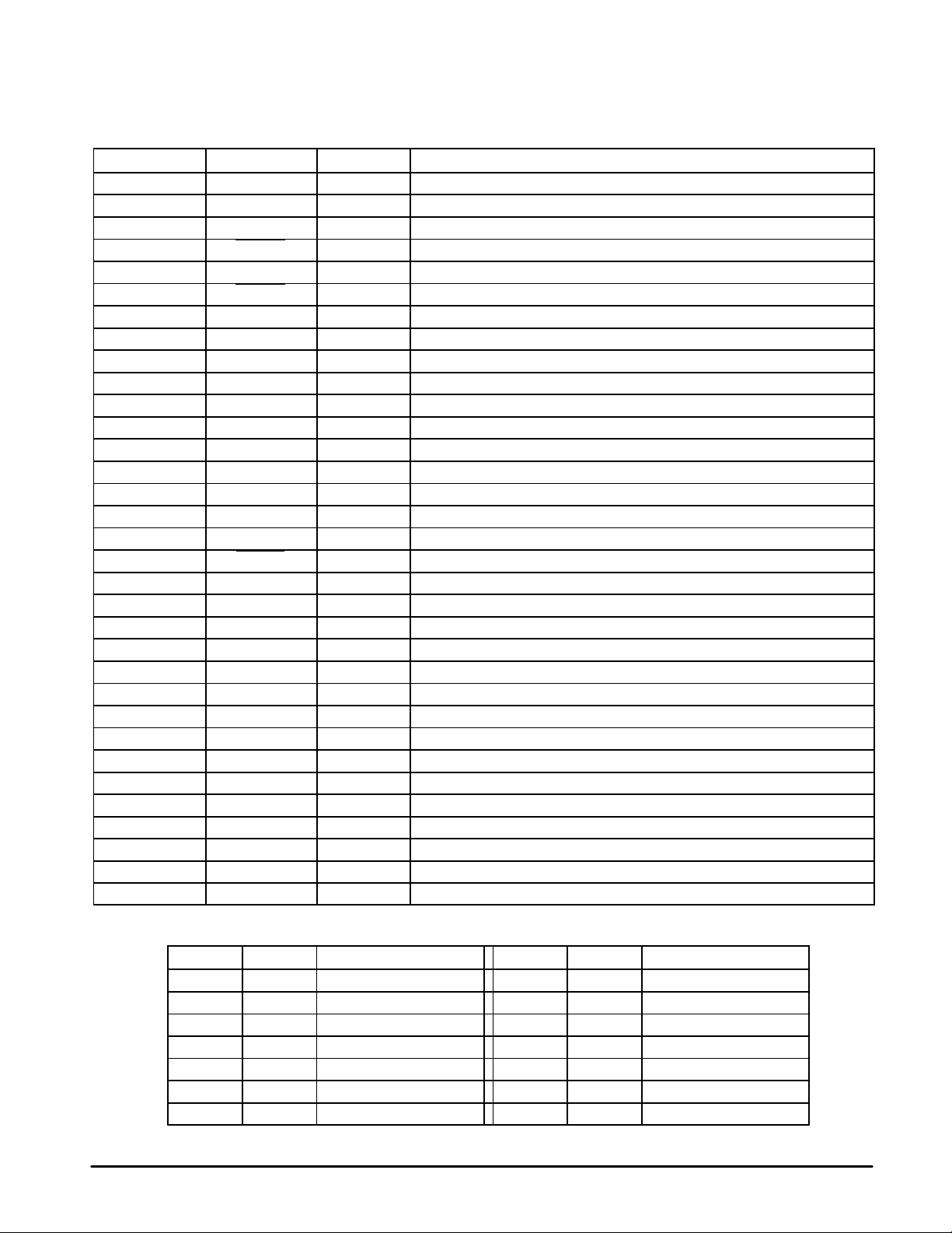
ELECTRICAL CHARACTERISTICS (The tested electrical characteristics are based on the conditions shown in Table 1 and 2.
Composite Video input signal = 1.0 Vpp, composed of: 0.7 Vpp Black–to–White; 0.3 Vpp Sync–to–Black; 0.3 Vpp Color Burst. V
= V
CC3
= 5.0 V, I
= 32 µA (Pin 9), unless otherwise noted.)
ref
Table 1. Control Bit Test Settings
Control Bit Name Value Function
$77–7 S–VHS–Y 0 Composite Video input selected.
$77–6 S–VHS–C 0 Composite Video input selected.
$77–5 FSI 0 50 Hz Field Rate selected.
$77–4 L2 GATE 0 PLL #2 Gating enabled.
$77–3 BLCP 0 Clamp Pulse Gating enabled.
$77–2 L1 GATE 0 Vertical Gating enabled.
$77–1, 0 CB1, CA1 1,1 Vertical section Auto–Countdown mode
$78–7 36/68 µs 0 Time from beginning of Line 4 to V ertical Sync is 36 µs.
$78–6 CalKill 0 Horizontal Calibration Loop enabled.
$79–7, 6 HI, VI 1,1 Normal
$7A–7 Xtal – 0 = 17.7 MHz crystal selected, 1 = 14.3 MHz crystal selected.
$7A–6 SSD 0 Normal
$7B–7, 6 T1, T2 1,1 Sound Trap Notch filter set to 5.5 MHz (with 17.7 MHz crystal).
$7C–7 SSC 0 Permits PAL and NTSC selection.
$7C–6, $7D–6 SSA, SSB – 0, 1 = PAL decoding, 1,0 = NTSC decoding
$7D–7, $7E–7, 6 P1, P3, P2 1, 1, 1 Sets Luma Peaking at 0 dB.
$7F–7, 6, $80–6 D3, D1, D2 0, 0, 0 Set Luma Delay to minimum
$80–7 RGB EN 0 Fast Commutate input can enable RGB inputs.
$81–7 Y2 EN 0 Y2 input (Pin 29) deselected
$81–6 Y1 EN 1 Y1 luma path from PAL/NTSC decoder selected.
$82–7 YUV EN 0 RGB output mode selected
$82–6 YX EN 0 Disable luma matrix from RGB inputs.
$83–7 L2 Gain 0 Set PLL #2 Phase/Frequency detector gain high.
$83–6 L1 Gain 1 Set PLL #1 Phase Detector gain high.
$84–7 H Switch 0 Set Horizontal Phase Detector filter switch open.
$84–6 525/625 – 0 = 625 lines (PAL), 1 = 525 lines (NTSC)
$85–7 F
$85–6 C
$86–7 Vin Sync 1 Composite Video inputs (Pin 1 or 3) Sync Source selected.
$86–6 H EN 0 Enabled Horizontal Timebase.
$87–7 Y2 Sync 0 Y2 sync source not selected.
$88–7 V2/V1 1 Select Video 1 input (Pin 1).
$88–6 RGB Sync 0 RGB inputs Sync Source not selected.
÷ 2 0 Select direct VCO output from PLL #2.
osc
Sync
0 16 Fh output selected at Pin 13.
CC1
= V
CC2
DAC Value Function DAC Value Function
$78 32 R–Y/B–Y Gain $82 32 Red Contrast Trim
$79 32 Sub Carrier Phase $83 32 Blue Brightness Trim
$7D 00 Blue Output DC Bias $84 32 Main Brightness
$7E 00 Red Output DC Bias $85 32 Red Brightness Trim
$7F 63 Pixel Clock VCO Gain $86 32 Saturation (Color Diff.)
$80 32 Blue Contrast Trim $87 16 Saturation (Decoder)
$81 32 Main Contrast $88 32 Hue
NOTE: Currents out of a pin are designated –, and those into a pin are designated +.
MOTOROLA ANALOG IC DEVICE DATA
Table 2. DAC Test Settings
3

MC44011
MAXIMUM RATINGS
Rating Symbol Value Unit
Power Supply Voltage V
Power Supply Difference
(Between any two VCC pins)
Input Voltage: Video 1, 2, SCL, SDL V
Input Voltage: 15 kHz Return –0.5, V
Input Voltage: R–Y, B–Y, Y2, RGB, FC –0.5, V
Junction T emperature (Storage and Operating) T
NOTES: 1. Devices should not be operated at these limits. The “Recommended Operating Conditions”
table provides for actual device operation.
2.ESD data available upon request.
CC1
V
CC2
V
CC3
– ±0.5 Vdc
in
J
RECOMMENDED OPERATING CONDITIONS
Characteristics Symbol Min Typ Max Unit
Power Supply Voltage V
Power Supply Difference (Between any two VCC pins) ∆V
Input Voltage: V ideo 1, 2 (Sync–White) V
Input Voltage: Chroma (S–VHS Mode) – – 1.2
Input Voltage: Y2 0.7 1.0 1.4
Input Voltage: RGB 0.5 0.7 1.0
Input Voltage: R–Y, B–Y (Pins 30, 31) 0 – 1.8
Input Voltage: 15 kHz Return 0 – V
Input Voltage: SCL, SDL 0 – V
Input Voltage: FC 0 – V
Input Voltage: Burst Signal 30 280 560 mVpp
Input Voltage: Sync Amplitude 60 300 V
Output Load Impedance to Ground: RGB (Pull–Up = 390 Ω) RL
Output Load Impedance to Ground: B–Y, R–Y RL
Output Load Impedance to Ground: Y1 RL
Pull–Up Resistance at Vertical Sync (Pin 4) R
Source Impedance: Video 1, 2 – 0 – 1.0 kΩ
Source Impedance: Pins 26 to 31 0 – 1.0
Pixel Clock Frequency (Pin 18, see PLL #2 Electrical Characteristic) f
15 kHz Return Pulse Width (Low Time) PW
I2C Clock Frequency f
Reference Current (Pin 9) I
Operating Ambient Temperature T
NOTE: All limits are not necessarily functional concurrently.
–0.5 to +6.0 Vdc
–0.5 to +6.0
–0.5 to +6.0
–0.5, V
–65 to +150 °C
+0.5 Vdc
CC1
+0.5
CC3
+0.5
CC2
CC1, 2, 3
CC
in
RGB
CD
Y1
VS
px
15k
I2C
ref
A
4.75 5.0 5.25 Vdc
–0.5 0 0.5 Vdc
0.7 1.0 1.4 Vpp
CC3
CC1
CC2
CC1
1.0 –
10 –
1.0 –
1.0 10 – kΩ
– 2.0 to 45 – MHz
0.2 – 45 µs
– – 100 kHz
– 32 – µA
0 – 70 °C
∞
∞
∞
Vdc
mVpp
kΩ
ELECTRICAL CHARACTERISTICS (T
Characteristics Min Typ Max Unit
POWER SUPPLIES
Power Supply Current (VCC = 5.0 V) Pin 40 75 95 115 mA
4
= 25°C, V
A
Pin 23 6.0 9.0 12
Pin 19 3.5 6.0 8.0
Total 85 110 135
CC1
= V
CC2
= V
= 5.0 V, unless otherwise noted.)
CC3
MOTOROLA ANALOG IC DEVICE DATA

MC44011
ELECTRICAL CHARACTERISTICS (continued) (T
Characteristics UnitMaxTypMin
PAL/NTSC/S–VHS DECODER
Video 1, 2 Inputs
Crosstalk Rejection, f = 1.0 MHz
(Measured at Y1 output, Luma Peaking = 0 dB, $77–7 = 1)
DC Level: @ Selected Input – 2.8 – Vdc
DC Level: @ Unselected Input – 0.7 –
Clamp Current –30 –20 –10 µA
Sound Trap Rejection (See Figures 14 to 23)
With 17.7 MHz Crystal: @ 6.5 MHz (T1, T2 = 00) 15 30 – dB
With 17.7 MHz Crystal: @ 6.0 MHz (T1, T2 = 10) 15 30 –
With 17.7 MHz Crystal: @ 5.5 MHz (T1, T2 = 11) 10 43 –
With 17.7 MHz Crystal: @ 5.74 MHz (T1, T2 = 01) 15 26 –
With 14.3 MHz Crystal: @ 4.44 MHz (T1, T2 = 11) – 35 –
R–Y, B–Y Outputs (Pins 41, 42)
Output Amplitude (with 100% Saturated Color Bars)
Saturation (DAC 87) = 00 – <1.0 – mVpp
Saturation (DAC 87) = 16 – 1.6 – Vpp
Saturation (DAC 87) = 63 1.8 3.0 –
DC Level During Blanking – 2.4 – Vdc
Hue Control – Minimum Phase (DAC 88 = 00) – –30 – Deg
Hue Control – Maximum Phase (DAC 88 = 63) – 30 –
Nominal Saturation (with respect to Y1 Output, Note 1) – 100 – %
R–Y/B–Y Ratio: Balance (DAC 78) = 63 1.35 1.69 2.06 V/V
B–Y/R–Y Ratio: Balance (DAC 78) = 32 0.98 1.27 1.58
B–Y/R–Y Ratio: Balance (DAC 78) = 00 0.60 0.77 0.96
Output Amplitude V ariation as Burst is varied from 80 mVpp to 600 mVpp – 3.0 – dB
Color Kill Attenuation ($7C–7, 6 and $7D–6 = 011) – 40 – dB
Crosstalk with respect to Y1 Output (@ 1.0 MHz) –27 –20 –
Chroma Subcarrier Residual
(Measured at Y1 Output, with 17.7 MHz Crystal)
f = Subcarrier – 25 60 mVpp
2nd Harmonic Residual – 4.0 12
4th Harmonic Residual – 12 30
(Measured at R–Y, B–Y Outputs, with 17.7 or 14.3 MHz Crystal)
f = Subcarrier – 5.0 20
2nd Harmonic Residual – 5.0 20
4th Harmonic Residual – 15 50
Y1 Luma Output (Pin 33)
Clamp Level 0.4 1.1 1.8 Vdc
Output Impedance – 300 – Ω
Composite Video Mode ($77–6, 7 = 00)
Output Level versus Input Level
Delay = 000, Peaking = 111, f = 100 kHz 1.0 1.1 1.2 V/V
Delay = Min–to–Max, Peaking = Min–to–Max – 1.1 –
–3.0 dB Bandwidth (17.7 MHz Crystal, PAL Decoding selected,
Sound trap at 6.5 MHz, Peaking off)
Peaking Range ($7D–7, $7E–6/7 = 000 to 111, @ 3.0 MHz, with 17.7 MHz Crystal,
Sound trap at 6.5 MHz)
Overshoot with Minimum Peaking – 0 – %
Differential Non–linearity (Measured with Staircase) – 2.0 – %
Delay (Pin 1 or 3 to 33)
With 14.3 MHz Crystal: Minimum – 690 – ns
Maximum – 1040 –
With 17.7 MHz Crystal: Minimum – 594 –
Maximum – 876 –
NOTE: 1. This spec indicates a correct output amplitude at Pins 41 and 42, with respect to Y1 output. For standard color bar inputs, the output amplitude is
NOTE: 1. between 1.5 and 1.7 Vpp, with the settings in T ables 1 and 2.
= 25°C, V
A
CC1
= V
CC2
= V
= 5.0 V, unless otherwise noted.)
CC3
20 40 – dB
– 2.8 – MHz
5.0 8.0 10 dB
MOTOROLA ANALOG IC DEVICE DATA
5

MC44011
ELECTRICAL CHARACTERISTICS
PAL/NTSC/S–VHS DECODER
S–VHS Mode ($77–6, 7 = 11)
Output Level versus Input Level (Delay = Min–to–Max) 1.0 1.1 1.2 V/V
–3.0 dB Bandwidth (17.7 MHz crystal, PAL Decoding selected,
Sound trap at 6.5 MHz)
Y/C Crosstalk Rejection 20 40 – dB
Delay (Luma input to Pin 33)
14.3 MHz Crystal: Minimum – 395 – ns
14.3 MHz Crystal: Maximum – 745 –
17.7 MHz Crystal: Minimum – 350 –
17.7 MHz Crystal: Maximum – 632 –
Crystal Oscillator
PLL Pull–in range with respect to Subcarrier Frequency
(Burst Level ≥ 30 mVpp): with 17.7 MHz Crystal – ±350 – Hz
(Burst Level ≥ 30 mVpp): with 14.3 MHz Crystal – ±300 –
4fsc Filter (Pin 44) DC Voltage
@ 14.3 MHz – 2.4 – Vdc
@ 17.7 MHz – 3.5 –
No Burst present – 1.3 –
DC Voltages Vdc
System Select (Pin 34)
NTSC Mode (SSA = 1, SSB = 0, SSC = 0, SSD = 0) 1.5 1.75 2.0
PAL Mode (SSA = 0, SSB = 1, SSC = 0, SSD = 0) 0 0.075 0.4
Color Kill Mode (SSA = 1, SSB = 1, SSC = 0, SSD = 0) – 0.075 –
External Mode (SSA = X, SSB = X, SSC = 1, SSD = 0) 3.7 4.0 4.3
Ident Filter (Pin 43)
NTSC Mode – 1.6 –
PAL Mode 1.2 1.5 1.8
No Burst present – 0.2 –
ACC Filter (Pin 2)
No Burst present – 0.25 –
Threshold for ACC Flag on 0.8 1.2 1.6
Burst = 50 mVpp – 1.4 –
Burst = 280 mVpp – 1.7 –
System Select Output Impedance – 40 100 kΩ
COLOR DIFFERENCE SECTION
RGB/YUV Outputs
Output Swing, Black–to–White (DAC $81 = 63) 2.0 3.0 – Vpp
THD (RGB Inputs to RGB Outputs @ 1.0 MHz, 0.7 Vpp) – 0.5 2.0 %
–3.0 dB Bandwidth – 6.0 – MHz
Clamp Level
RGB Outputs ($7D, 7E = 00) – 1.4 – Vdc
UV Outputs ($7D, 7E = 32) – 2.3 –
Red, Blue Clamp Level Change (DACs $7D, 7E varied from 00 to 63) 0.85 1.8 2.4
Crosstalk Rejection
Among RGB Outputs @ 1.0 MHz 20 40 – dB
Y1 to Y2 20 40 –
From RGB Outputs to Y1 or Y2 20 40 –
Input Black Clamp Voltage at Y2, B–Y, R–Y, and RGB 2.4 3.0 3.6 Vdc
Fast Commutate Input (Pin 25)
Switching Threshold Voltage – 0.5 – Vdc
Input Current @ Vin = 0 V – –7.5 – µA
Input Current @ Vin = 5.0 V – 0 –
Timing: Input Low–to–High (RGB Enable) – 50 – ns
Timing: Input High–to–Low (RGB Disable) – 90 –
(continued) (TA = 25°C, V
Characteristics UnitMaxTypMin
CC1
= V
CC2
= V
= 5.0 V, unless otherwise noted.)
CC3
– 4.5 – MHz
6
MOTOROLA ANALOG IC DEVICE DATA

MC44011
ELECTRICAL CHARACTERISTICS (continued) (T
Characteristics UnitMaxTypMin
COLOR DIFFERENCE SECTION
Contrast (Gain) V/V
Y1 to RGB (DAC $81 = 32, DAC $86 = 00) 1.9 2.4 3.0
Y2 to RGB (DAC $81 = 32, DAC $86 = 00) 1.8 2.3 2.8
Green In (Pin 27) to Green Out (Pin 21) with YX Enabled 1.8 2.3 2.4
($82–6 = 1, DAC $81 and DAC $86 = 32)
Red–to–Green and Blue–to–Green Gain Ratio 0.8 1.0 1.2
RGB Input to RGB Output with YX Not Enabled 2.0 2.6 3.2
($82–6 = 0, DAC $81 and DAC $86 = 32)
Ratio (DAC $81 = 00 versus 32) – 0.2 0.4
Ratio (DAC $81 = 63 versus 32) 1.5 2.0 2.5
Red and Blue Trim Control (DACs $80, 82 varied from 00 to 63) ±5.0 ±30 ±60 %
Saturation (Average of R, G, B saturation levels with respect to Luma)
Inputs at Pins 29 to 31 (DAC $86 = 32) 50 90 130 %
Ratio (DAC $86 = 00 versus 32) – – 5
Ratio (DAC $86 = 63 versus 32) 150 170 190
Inputs at Pins 26 to 28 (DAC $86 = 32, $82–6 = 1) 70 125 180
Brightness
Black Level Range (Brightness = 00 to 63 with respect to Brightness setting of 32) ±0.3 ±0.5 ±0.7 Vdc
Red and Blue Trim Control (DACs $83, 85 varied from 00 to 63) ±0.05 ±0.3 ±0.6
Color Coefficients
G–Y Matrix Coefficient versus B–Y –0.21 –0.19 –0.17
G–Y Matrix Coefficient versus R–Y –0.56 –0.51 –0.46
YX Matrix (Inputs at Pins 26 to 28, $82–6 = 1):
Y versus R 0.28 0.30 0.32
Y versus G 0.57 0.59 0.61
Y versus B 0.09 0.11 0.13
HORIZONTAL TIME BASE SECTION (PLL #1)
Free–Running Period (Calibration mode in effect, Bit $86–6 = 1)
17.7 MHz Crystal selected ($84–6 = 0) 62.5 64.0 65.5 µs
14.3 MHz Crystal selected ($84–6 = 1) 62.5 63.5 65.5
VCO minimum period (Pin 11 Voltage at 1.2 V) 56 59.5 62 µs
VCO maximum period (Pin 11 Voltage at 2.8 V) 66 69.5 72
VCO Control Gain factor 5.0 8.5 12 µs/V
Phase Detector Current
High Gain ($83–6 = 1)
Low Gain–to–High Gain Current Ratio 0.32 0.38 0.44 µA/µA
Noise Gate Width ($77–2 = 0, Low Gain, see Figure 26) – 16 – µs
Horizontal Filter Switch (Pin 12)
Saturation Voltage (I12 = 20
Dynamic Impendance ($84–7 = 1) – <5.0 – kΩ
Parallel Resistance ($84–7 = 0) 0.6 1.0 – MΩ
Pins 8, 13, 14 Output Level
High (lO = –40 µA)
Low (lO = 800 µA) – 0.1 0.8
Burst Gate (Pin 8) Timing (See Figures 25, 27) µs
Rising edge from Sync leading edge (Pins 1, 3) 4.4 5.6 6.8
Rising edge from Sync center (Pins 26 to 29) – 2.5 –
Pulse Width 3.0 3.5 4.0
16Fh Output (Pin 13) Timing (Bit $85–6 = 0) (See Figures 25, 27)
Rising edge from Fh rising edge – 1.3 – µs
Duty Cycle – 50 – %
Composite Sync Output (Pin 13) Timing (Bit $85–6 = 1) µs
Input Sync center to Output Sync center (Pins 1, 3) – 0.95 –
Input Sync center to Output Sync center (Pins 26 to 29) – 0.4 –
µA)
= 25°C, V
A
CC1
= V
CC2
= V
= 5.0 V, unless otherwise noted.)
CC3
15 50 85 µA
– 10 100 mV
2.4 4.5 – Vdc
MOTOROLA ANALOG IC DEVICE DATA
7

MC44011
ELECTRICAL CHARACTERISTICS
HORIZONTAL TIME BASE SECTION (PLL #1)
Fh Reference (Pin 14) Timing (See Figures 25, 27)
Rising edge from Sync center (Pins 1, 3) – 1.3 – µs
Rising edge from Sync center (Pins 26 to 29) – 650 – ns
Duty cycle – 50 – %
Sandcastle Output (Pin 35, see Figures 25, 27) Vdc
Output Voltage – Level 1 3.7 4.0 4.3
Output Voltage – Level 2 2.8 3.0 3.2
Output Voltage – Level 3 – 1.55 –
Output Voltage – Level 4 – 0.07 –
Rising edge from Sync center (Pins 1, 3) – –2.6 – µs
Rising edge from Sync center (Pins 26 to 29) – –3.3 –
High Time – 6.0 –
Level 2 Time – 5.0 –
Reference Voltage @ Pin 9 (I
PHASE–LOCKED PIXEL CLOCK SECTION (PLL #2)
VCO Frequency @ Pin 18 MHz
Minimum (Pin 16 = 1.6 V , $85–7 = 1) – 2.0 4.0
Maximum (Pin 16 = 4.0 V , $85–7= 0) 30 45 60
VCO Up (Flag 19) Threshold Voltage @ Pin 16 1.5 1.7 1.9 Vdc
VCO Down (Flag 20) Threshold Voltage @ Pin 16 3.1 3.3 3.5
VCO Control Voltage Range @ Pin 16 1.2 – 3.8 Vdc
VCO Control Gain factor ($7FDAC = 00, $85–7 = 0) 4.0 8.0 12 MHz/V
Charge Pump Current (Pin 16) 25 50 75 µA
High Gain ($83–7 = 0)
Current Ratio 0.3 0.4 0.5 µA/µA
Low Gain–to–High Gain
Pixel Clock Output (Pin 18) (Load = 3 FAST TTL loads + 10 pF)
Output Voltage – High – 3.9 – Vdc
Output Voltage – Low – 0.15 –
Rise Time @ 50 MHz – 7.0 – ns
Rise Time @ 9.0 MHz – 17 –
Fall Time @ 50 MHz – 5.0 –
Fall Time @ 9.0 MHz – 8.0 –
15 kHz Return (Pin 15)
Input Threshold Voltage – 1.5 – Vdc
Falling edge from Fh rising edge – 60 – ns
Minimum Input Low Time 200 – –
VERTICAL DECODER
Vertical Frequency Range 43.3 – 122 Hz
Vertical Sync Output
Saturation Voltage (lO = 800 µA) – 0.1 0.8 V
Leakage Current @ 5.0 V (Output high) – – 40 µA
Timing from Sync polarity reversal to Pin 4 falling edge (See Figures 33, 34) µs
($78–7 = 0) 32 36 40
($78–7 = 1) 62 68 74
Vertical Sync Pulse Width (Pin 4, NTSC or PAL) 490 500 510 µs
Field Ident (Pin 7) Output Voltage – High (lO = –40 µA) 2.4 4.5 – Vdc
Field Ident (Pin 7) Output Voltage – Low (lO = 800 µA) – 0.1 0.8
Field Ident (Pin 7) Timing – Fig. 33, 34 –
HORIZONTAL SYNC SEPARATOR
Sync Slicing Levels (Pins 1, 3) – 120 – mV
From Black Levelāā(Pins 26 to 29)
ref
(continued) (TA = 25°C, V
Characteristics UnitMaxTypMin
= 32 µA) 1.0 1.2 1.4 Vdc
CC1
= V
CC2
= V
= 5.0 V, unless otherwise noted.)
CC3
– 150 –
8
MOTOROLA ANALOG IC DEVICE DATA
FB FN
Representative Circuitry
Description
QFP PLCC
Pin
39, 41 1, 3
Video
Input
MC44011
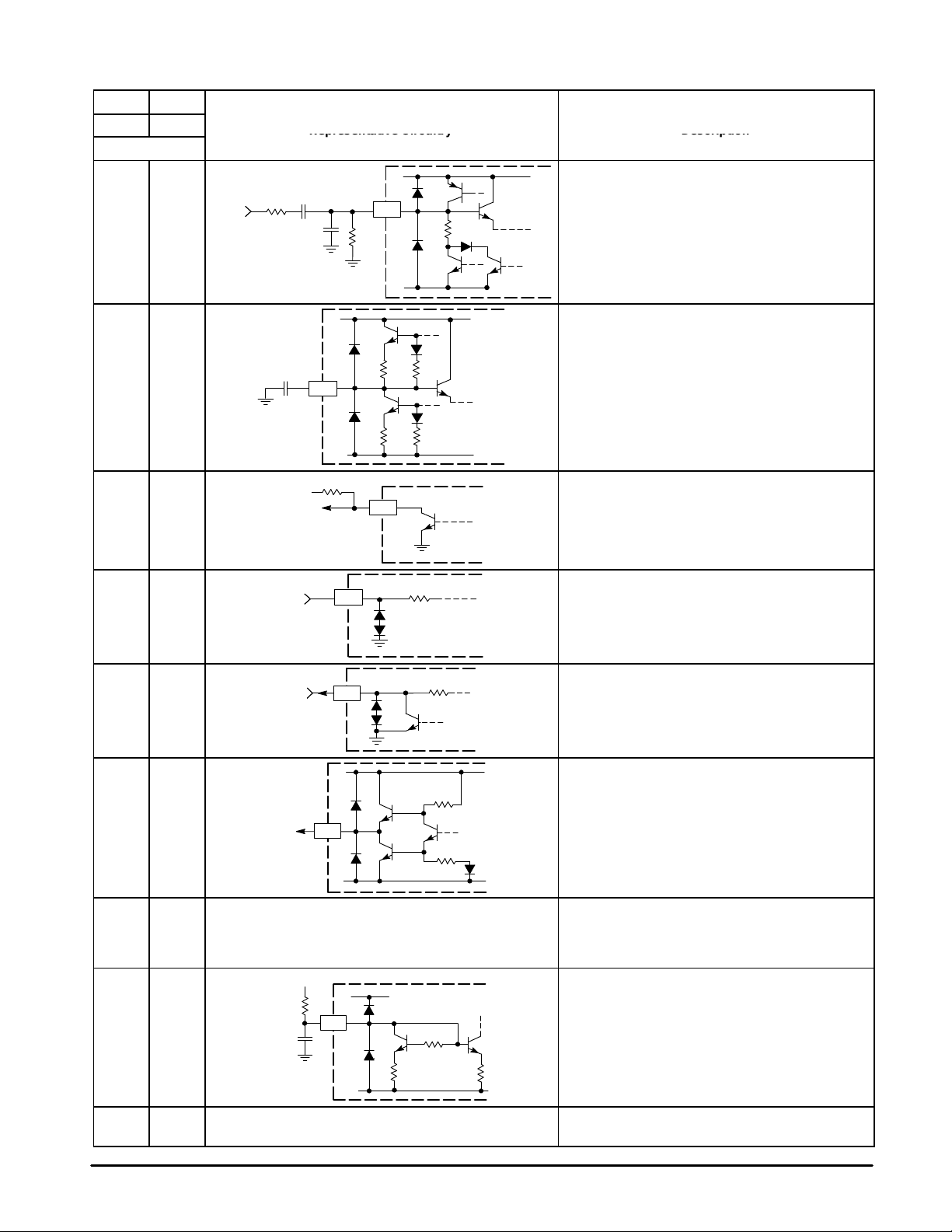
PIN FUNCTION DESCRIPTION
Representative Circuitry Description
(Pin numbers refer to PLCC package)
0.47
470
47 pF
10 M
20 k
(Pin numbers refer to PLCC package)
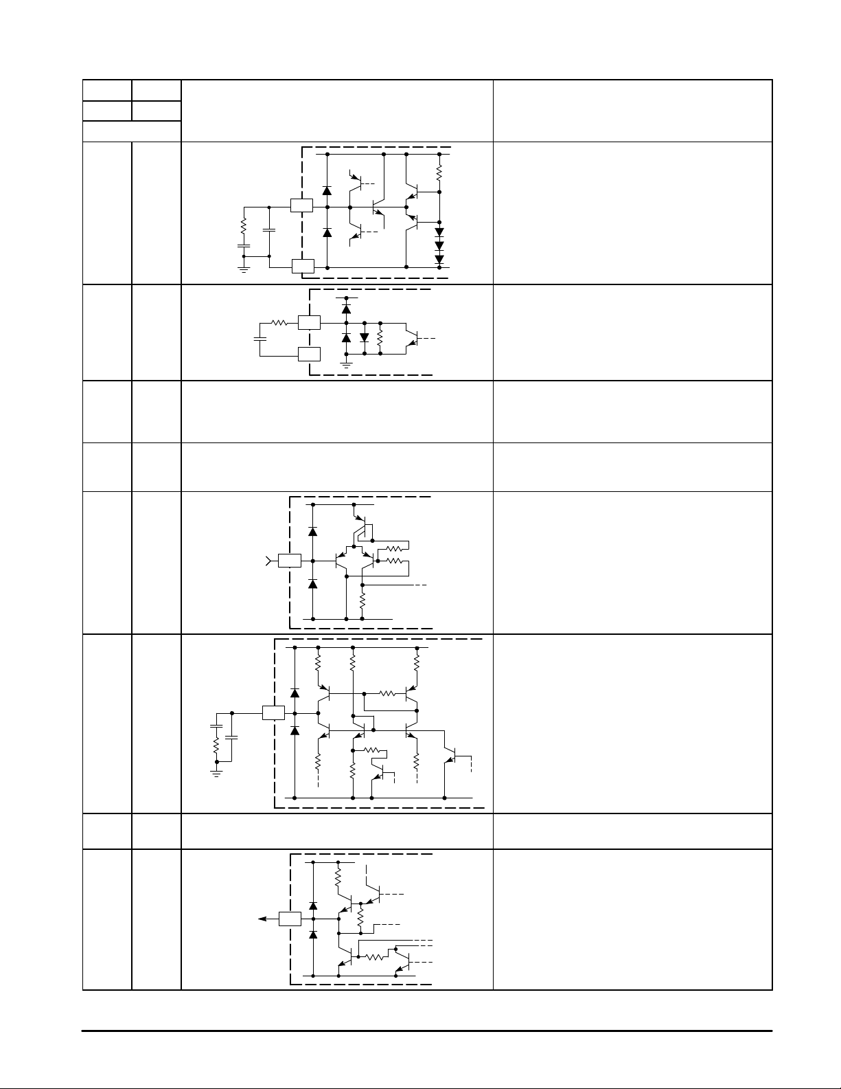
Video Input 1 & 2 – Video 1 (Pin 1) and Video 2
(Pin 3) are composite video inputs. Either can be
NTSC or PAL. Input impedance is high, termination
must be external. Also used for the luma and chroma
components of an S–VHS signal. Selection of these
inputs is done by software. External components
protect against ESD and noise.
40 2
42 4
43 5
44 6
0.1
5.0
Vertical Sync
From MCU
To/From MCU
2
10 k
ACC Filter – A 0.1 µF capacitor at this pin filters the
feedback loop of the chroma automatic gain control
amplifier. Input chroma burst amplitude can be
between 30 and 600 mVpp.
Vertical Sync Output – An open collector output
4
5
6
100 k
180 k
requiring an external pull–up. Output is an active low
pulse, 500 µs wide, occurring each field. Timing of this
pulse depends on Bit $78–7.
SCL – Clock for the I2C bus interface. See Appendix C
for specifications. Maximum frequency is 100 kHz.
SDL – Bidirectional data line for the I2C bus interface.
As an output, it is an open collector. (Write Address
$8A, Read Address $8B)
1 7
7
(Same as Pin 7)
5.0
9
2 8
3 9
4 10
Field ID
110 k
2.2 µF / /
0.01
(See power distribution diagram at the end of this section.)
MOTOROLA ANALOG IC DEVICE DATA
8.0 k
100 k
20 k
12 k
Field ID – TTL level output indicating Field 1 or Field 2.
Polarity depends on state of Bit $78–7 (Vertical Sync
Delay). See T able 1 1 and Figure 33 and 34.
Burst Gate – TTL level output used for external
clamps, as well as internally. Pulse is active high,
≈ 3.5 µs wide, with the rising edge ≈ 3.0 µs after
center of selected incoming sync pulse.
Reference Current Input – Current supplied to this
pin, typically 32 µA from 5.0 V through a 110 kΩ
resistor, is the reference current for the calibration
circuit. Noise filtering should be done at the pin.
Voltage at this pin is typically 1.2 V.
Quiet Ground – Ground for the horizontal PLL filter
(PLL #1) at Pin 1 1.
9
FB FN
QFP
PLCC
Pin
5 11
PIN FUNCTION DESCRIPTION (continued)
Representative Circuitry
Representative Circuitry
(Pin numbers refer to PLCC package)
(Pin numbers refer to PLCC package)
11
100 k
0.1
68 pF
10
MC44011
Description
(Pin numbers refer to PLCC package)
(Pin numbers refer to PLCC package)
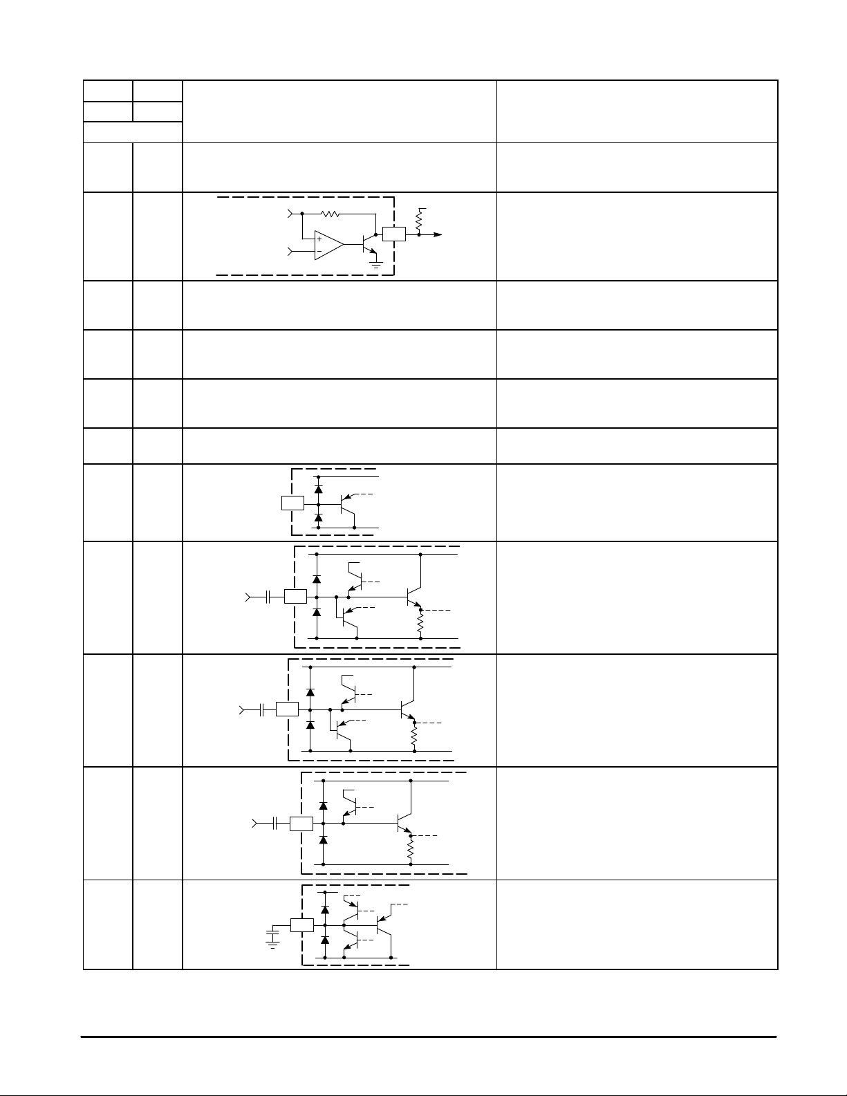
H Filter – Components at this pin filter the output of
the phase detector of PLL #1. This PLL becomes
phase–locked to the selected incoming horizontal
sync. External component values are valid for NTSC
and PAL systems.
Description
6 12
7 13
8 14
9 15
10 16
0.047
10 k
470 pF
15 kHz
Return
4700 pF
12 k
12
(Same as Pin 7)
(Same as Pin 7)
15
16
11
Down
1.0 k
6.0 k
6.0 k
1.0 M
10 k
20 k
UpGain
Vert
Gate
H Filter Switch – An internal switch–to–ground which
permits altering the filtering action of the components
at Pin 11.
16 Fh/C
pin provides either a square wave equal to Fh x 16
(≈ 250 kHz), or composite sync, depending on the
setting of Bit $85–6.
Fh Reference – A TTL square wave output which is
phase–locked to the selected incoming horizontal sync.
The rising edge occurs ≈ 1.3 µs after sync center.
15 kHz Return – This TTL input receives the output of
an external frequency divider which is part of PLL #2
(Pixel Clock PLL). This signal will be phase and
frequency–locked to the Fh signal at Pin 14. If PLL #2
is not used, this pin should be connected to a 5.0 V
supply.
PLL #2 Filter – Components at this pin filter the output
of the phase detector of PLL 2. This PLL becomes
phase–locked to the Fh signal at Pin 14.
Recommended values for filter components are
shown. External components should be connected to
ground at Pin 17. If PLL #2 is not used, this pin should
be grounded.
– A TTL level output from PLL #1. This
Sync
11 17
12 18
10
(See power distribution diagram at the end of this section.)
200
Pixel
Clock
Output
18
Gnd3 – Ground for the high frequency PLL #2. Signals
at Pins 15 to 19 should be referenced to this ground.
Pixel Clock Output – Sampling clock output (TTL) for
external A/D converters, and for the external frequency
divider. Frequency range at this pin is 6.0 to 40 MHz.
MOTOROLA ANALOG IC DEVICE DATA
FB FN
QFP
PLCC
Pin
13 19
14 20
MC44011
PIN FUNCTION DESCRIPTION (continued)
Representative Circuitry
Representative Circuitry
(Pin numbers refer to PLCC package)
(Pin numbers refer to PLCC package)
(See power distribution diagram at the end of this section.)
20
5.0 V
390
Output
Color
& Gain
Brightness
36 k
Description
(Pin numbers refer to PLCC package)
(Pin numbers refer to PLCC package)
V
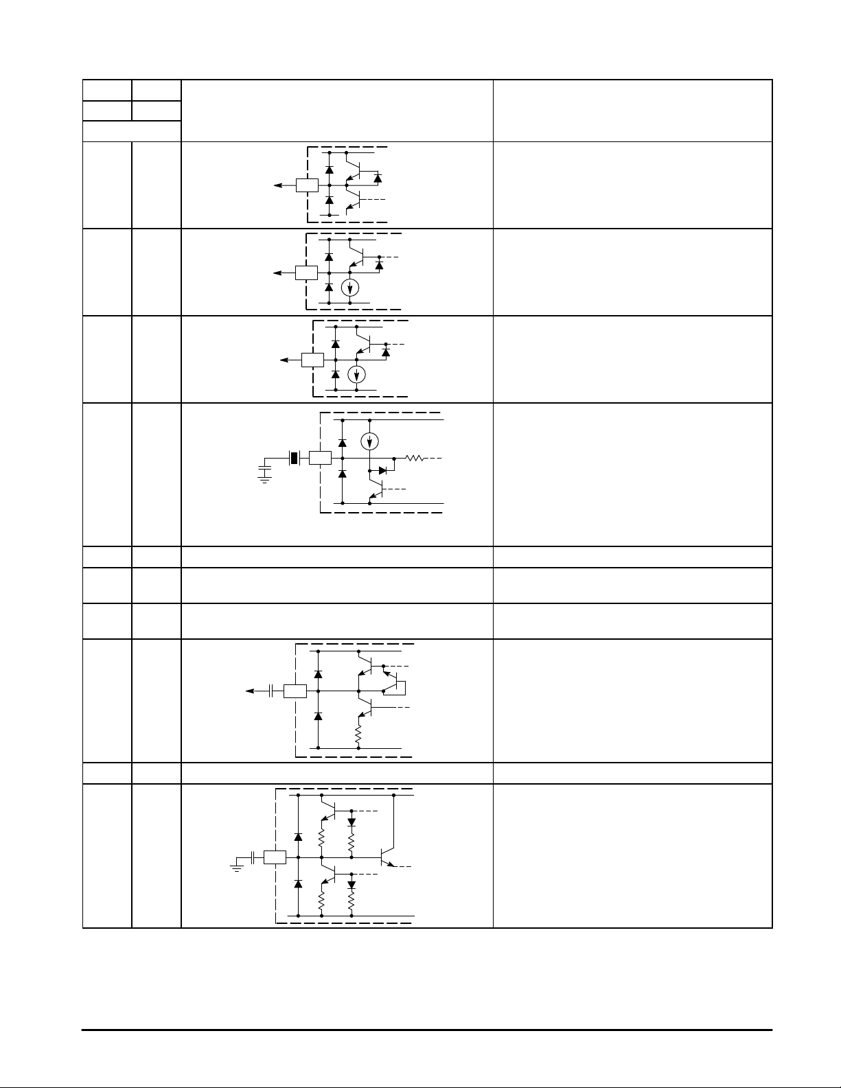
– A 5.0 V supply (±5%), for the high frequency
CC3
PLL #2. Decoupling must be provided from this pin to
Pin 17. Ripple on this pin will affect pixel clock jitter.
R/V Output – Red (in RGB mode), or R–Y (in YUV
mode), output from the color difference stage. A
pull–up (390 Ω) to 5.0 V is required. Blank level is
≈ 1.4 Vdc. Maximum amplitude is ≈ 3.0 Vpp,
black–to–white.
Description
15 21
16 22
17 23
18 24
19 25
20, 21,2226, 27,
28
23 29
(Same as Pin 20)
(Same as Pin 20)
(See power distribution diagram at the end of this section.)
(See power distribution diagram at the end of this section.)
25
V
ref
R, G, B
Inputs
100 k
V
ref
Y2
Input
29
100 k
G/Y Output – Green (in RGB mode), or Y (in YUV
mode), output from the color difference stage (same
as Pin 20).
B/U Output – Blue (in RGB mode), or B–Y (in YUV
mode), output from the color difference stage (same
as Pin 20).
V
– A 5.0 V supply (±5%), for the color difference
CC2
stage. Decoupling must be provided from this pin to
Pin 24.
Gnd2 – Ground for the color difference stage. Signals
at Pins 20 to 31 should be referenced to this pin.
FC – Fast Commutate switch. Taking this pin high
(TTL level) connects the RGB inputs (Pins 26 to 28)
to the RGB outputs (Pins 20 to 22), permitting an
overlay function. The switch can be disabled in
software (Bit $80–7).
Blue (26), Green (27), Red (28) Inputs – Inputs to
the color difference stage. Designed to accept
standard analog video levels, these input pins have a
clamp and sync separator. They are selected with
Pin 25 or in software (Bit $80–7).
Y2 Input – Luma #2/Composite sync input. This
luma input to the color difference stage is used in
conjunction with auxiliary color difference inputs,
and/or as a sync input. Clamp and sync separator
are provided.
24, 25 30, 31
R–Y, B–Y
Inputs
26 32
0.47
32
MOTOROLA ANALOG IC DEVICE DATA
B–Y (30), R–Y (31) Inputs – Inputs to the color
V
ref
100 k
difference stage. Designed for standard color
difference levels, these inputs can be capacitor
coupled from the color difference outputs, from a delay
line, or an auxiliary signal source. Input clamp is
provided.
Y1 Clamp – A 0.47 µF capacitor at this pin provides
clamping for the Luma #1 output.
11
FB FN
QFP
PLCC
Pin
27 33
MC44011
PIN FUNCTION DESCRIPTION (continued)
Representative Circuitry
Representative Circuitry
(Pin numbers refer to PLCC package)
(Pin numbers refer to PLCC package)
Y1
Output
33
Description
(Pin numbers refer to PLCC package)
(Pin numbers refer to PLCC package)
Y1 Output – Luma #1 output. This output from the
PAL/NTSC/S–VHS decoder is the luma component of
the decoded composite video at Pin 1 or 3. It is
internally directed to the color difference stage.
Description
28 34
System
Select
29 35
Sandcastle
Pulse
30, 32 36, 38
R = 400 Ω at Pin 38
Ω
R = 300
31 37 No Connect – This pin is to be left open.
33 39
34 40
35 41
(See power distribution diagram at the end of this section.)
(See power distribution diagram at the end of this section.)
at Pin 36
B–Y
34
35
14.3 MHz
17.7 MHz
41
20 µA
R
System Select – A multi–level dc output which
indicates the color decoding system to which the
PAL/NTSC detector is set by the software. This output
is used by the MC44140 chroma delay line.
Sandcastle Pulse – A multi–level timing pulse output
used by the MC44140 chroma delay line. This pulse
encompasses the horizontal sync and burst time.
Xtal 2 (36), Xtal 1 (38) – Designed for connection of 4x
subcarrier color crystals. Selection is done in software.
The selected frequency is used by the PAL/NTSC
detector; system identifier; all notches and traps; delay
lines; and the horizontal calibration circuit.
The crystal frequency should be:
14.3 MHz at Pin 36 for NTSC,
17.7 MHz at Pin 38 for PAL.
(See Table 17 for crystal specifications)
Ground 1 – Ground for all sections except PLL #2
and the color difference stage.
V
– A 5.0 V (±5%), supply to all sections except
CC1
PLL #2 and the color difference stage.
B–Y Output – Output from the PAL/NTSC decoder, it
is typically capacitor–coupled to a delay line or to the
B–Y input. This pin is clamped, and filtered at the
color subcarrier frequency , 2x, and 8x that frequency.
36 42 (Same as Pin 41) R–Y Output – Output from the PAL/NTSC decoder.
37 43
0.1
43
12
Ident Filter – A 0.1 µF capacitor filters the system
identification circuit in the NTSC/PAL decoder.
MOTOROLA ANALOG IC DEVICE DATA
FB FN
QFP
PLCC
Pin
38 44
MC44011
PIN FUNCTION DESCRIPTION (continued)
Representative Circuitry
Representative Circuitry
(Pin numbers refer to PLCC package)
(Pin numbers refer to PLCC package)
0.1
47 k
2200 pF
44
Description
(Pin numbers refer to PLCC package)
(Pin numbers refer to PLCC package)
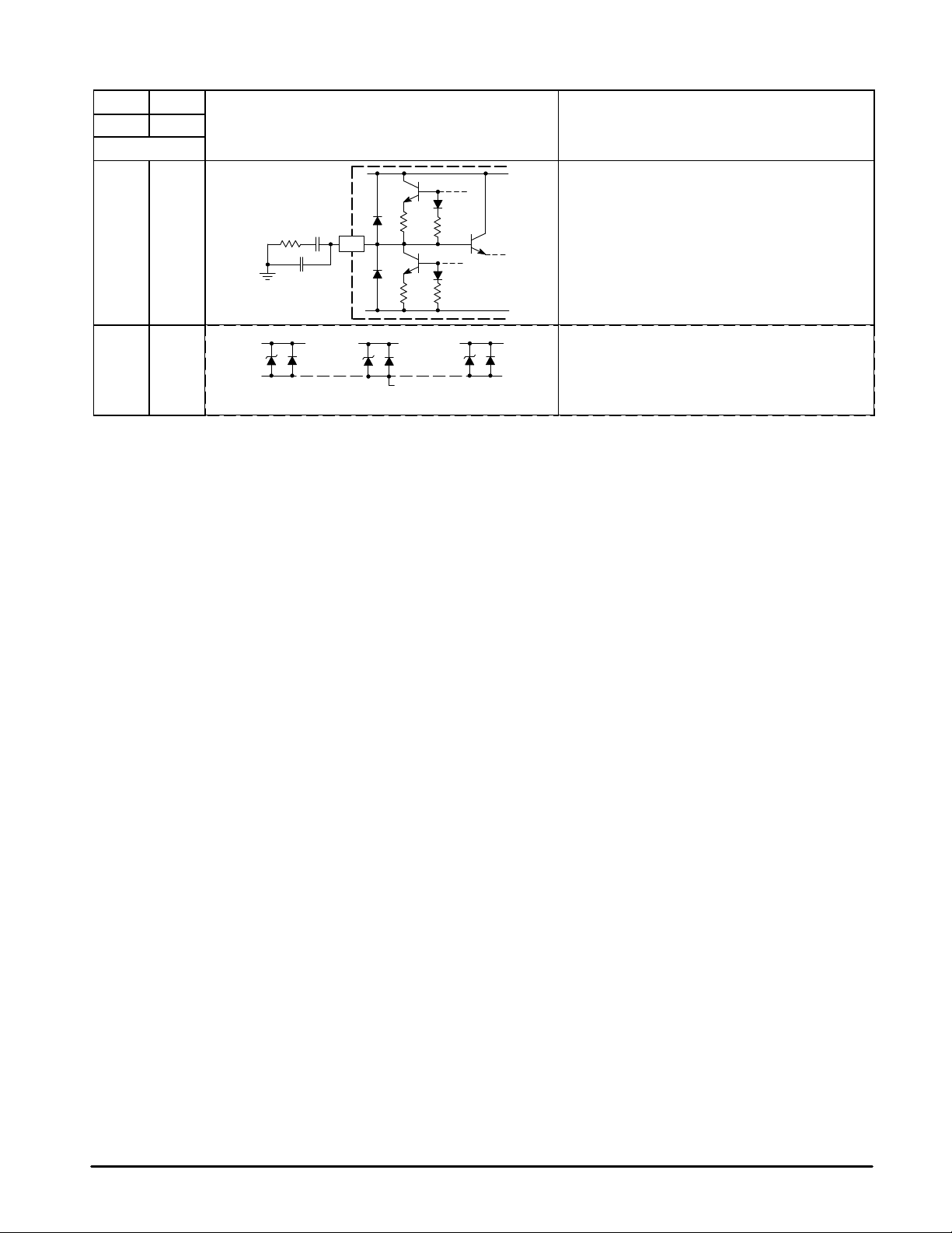
Crystal PLL Filter – Components at this pin filter the
PLL for the crystal chroma oscillator circuit.
Description
4, 11,
13, 17,
18, 33,
34
10, 17,
19, 23,
24, 39,
40
V
CC1
7.0 V
(Dashed lines indicate substrate connection.)
7.0 V
V
CC2
7.0 V
V
CC3
Power Distribution – The three VCC pins must be
externally connected to 5.0 V (±5%) supply. The four
grounds must be externally tied together, preferably to
a ground plane.
MOTOROLA ANALOG IC DEVICE DATA
13
10
MC44011
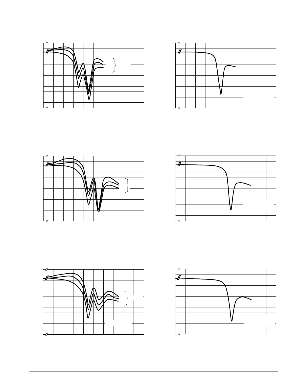
Luma Frequency Response (14.3 MHz) Crystal, (4.5 MHz) Sound Trap
Figure 2. Composite Video Mode Figure 3. S–VHS Mode
10
0
–10
–20
–30
–40
dB GAIN AT Y1 RELATIVE TO VIDEO 1
–50
0.1
10
0
–10
–20
–30
–40
dB GAIN AT Y1 RELATIVE TO VIDEO 1
–50
0.1
0
000
Peaking
010
111
Sound Trap = 1,1
1.0 3.0 5.0 7.0 10
f, FREQUENCY (MHz)
–10
–20
–30
–40
dB GAIN AT Y1 RELATIVE TO VIDEO 1
–50
0.1 1.0 3.0 5.0 7.0 10
f, FREQUENCY (MHz)
Sound Trap = 1,1
All Peaking Settings
Luma Frequency Response (17.7 MHz) Crystal, (5.5 MHz) Sound Trap
Figure 4. Composite Video Mode Figure 5. S–VHS Mode
10
0
000
Peaking
010
111
Sound Trap = 1,1
1.0 3.0 5.0 7.0 10 0.1 1.0 3.0 5.0 7.0 10
f, FREQUENCY (MHz) f, FREQUENCY (MHz)
–10
–20
–30
–40
dB GAIN AT Y1 RELATIVE TO VIDEO 1
–50
Sound Trap = 1,1
All Peaking Settings
10
0
–10
–20
–30
–40
dB GAIN AT Y1 RELATIVE TO VIDEO 1
–50
0.1
14
Luma Frequency Response (17.7 MHz) Crystal, (5.5/5.75 MHz) Sound Trap
Figure 6. Composite Video Mode
000
Peaking
010
111
Sound Trap = 1,1
1.0 3.0 5.0 7.0 10
f, FREQUENCY (MHz)
10
0
–10
–20
–30
Sound Trap = 0,1
–40
dB GAIN AT Y1 RELATIVE TO VIDEO 1
–50
0.1 1.0 3.0 5.0 7.0 10
f, FREQUENCY (MHz)
All Peaking Settings
MOTOROLA ANALOG IC DEVICE DATA
Figure 7. S–VHS Mode
MC44011
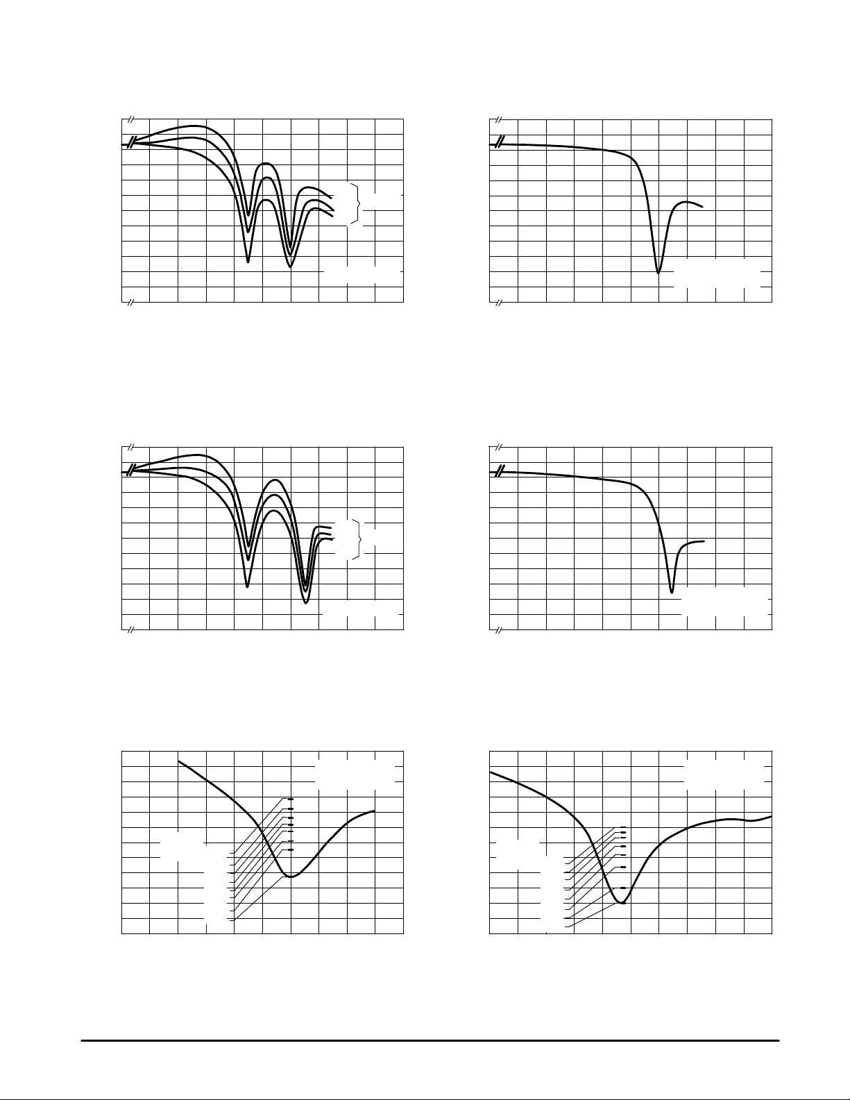
Luma Frequency Response (17.7 MHz) Crystal, (6.0 MHz) Sound Trap
Figure 8. Composite Video Mode
10
0
–10
000
Peaking
–20
010
111
–30
–40
dB GAIN AT Y1 RELATIVE TO VIDEO 1
–50
0.1 1.0 3.0 5.0 7.0 10 0.1 1.0 3.0 5.0 7.0 10
Sound Trap = 1,0
10
0
–10
–20
–30
–40
dB GAIN AT Y1 RELATIVE TO VIDEO 1
–50
Figure 9. S–VHS Mode
Sound Trap = 1,0
All Peaking Settings
f, FREQUENCY (MHz)f, FREQUENCY (MHz)
Luma Frequency Response (17.7 MHz) Crystal, (6.5 MHz) Sound Trap
Figure 10. Composite Video Mode Figure 11. S–VHS Mode
10
–10
–20
–30
0
000
Peaking
010
111
10
0
–10
–20
–30
–40
dB GAIN AT Y1 RELATIVE TO VIDEO 1
–50
0.1
–10
–15
–20
–25
–30
–35
dB GAIN AT Y1 RELATIVE TO VIDEO 1
–40
3.0
Sound Trap = 0,0
All Peaking Settings
Sound Trap = 0,0
–40
dB GAIN AT Y1 RELATIVE TO VIDEO 1
–50
1.0 3.0 5.0 7.0 10 1.0 3.0 5.0 7.0 10
0.1
f, FREQUENCY (MHz) f, FREQUENCY (MHz)
Figure 12. (3.58 MHz) Chroma Notch Figure 13. (4.43 MHz) Chroma Notch
–10
Gain at
Peaking =
000
001
100
101
010
011
110
111
Sound Trap = 1,1
14.3 MHz Crystal
–15
–20
–25
Gain at
Peaking =
–30
–35
dB GAIN AT Y1 RELATIVE TO VIDEO 1
3.5 4.0 4.5 5.0
–40
4.0
000
001
100
101
010
011
110
111
f, FREQUENCY (MHz)f, FREQUENCY (MHz)
Sound Trap = 1,1
17.7 MHz Crystal
MOTOROLA ANALOG IC DEVICE DATA
15
–15
MC44011
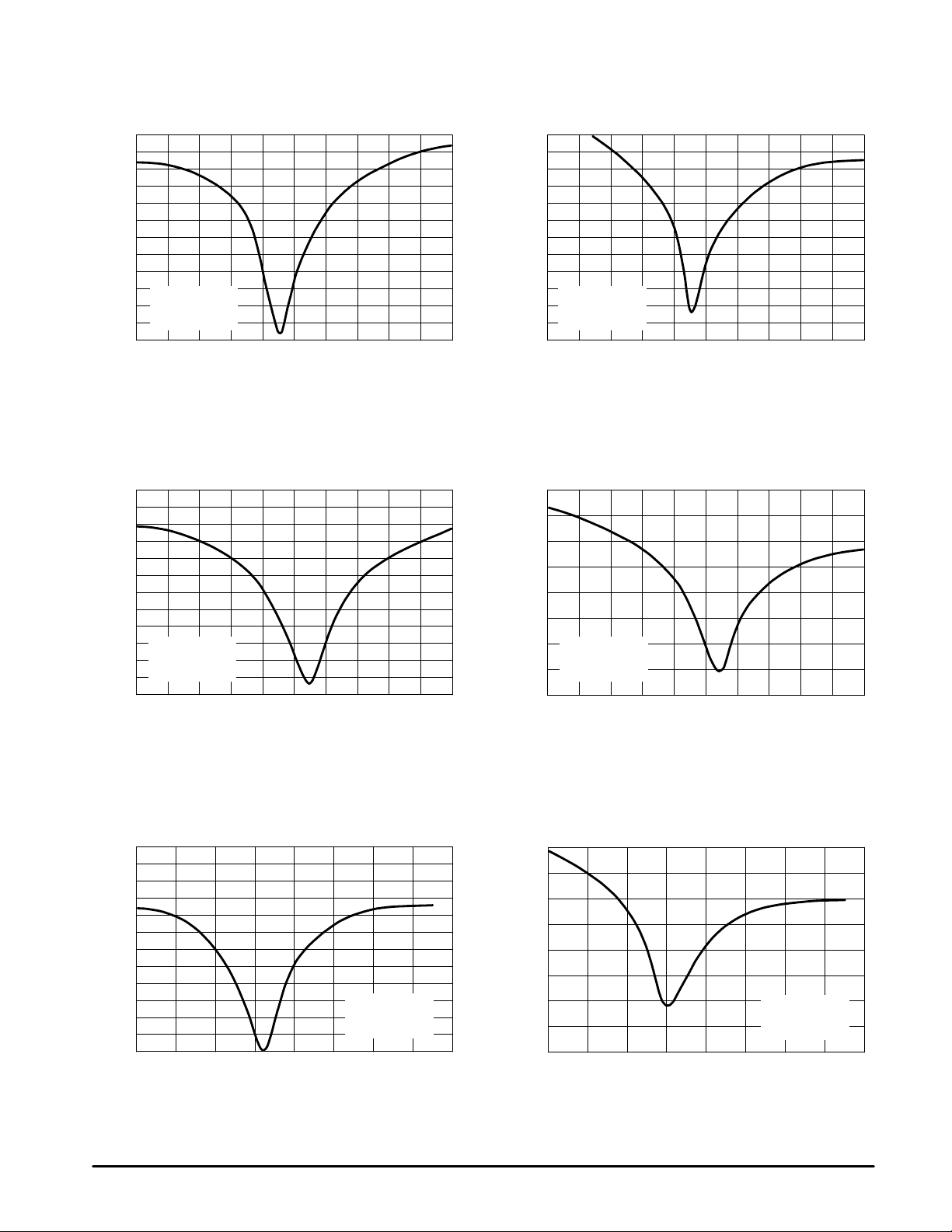
(4.5 MHz) Sound Trap
Figure 14. Composite Video Mode Figure 15. S–VHS Mode
–10
–20
–25
–30
–35
–40
dB GAIN AT Y1 RELATIVE TO VIDEO 1
–45
4.0
–15
–20
–25
–30
–35
–40
dB GAIN AT Y1 RELATIVE TO VIDEO 1
–45
5.0
–15
–20
–25
–30
Sound Trap = 1,1
Peaking = 111
14.3 MHz Crystal
dB GAIN AT Y1 RELATIVE TO VIDEO 1
4.5 5.0 4.0 4.5 5.0
Sound Trap = 1,1
–35
Peaking = 111
14.3 MHz Crystal
–40
f, FREQUENCY (MHz)f, FREQUENCY (MHz)
(5.5 MHz) Sound Trap
Figure 16. Composite Video Mode Figure 17. S–VHS Mode
–5.0
–10
–15
–20
–25
–30
–35
Sound Trap = 1,1
Peaking = 111
17.7 MHz Crystal
dB GAIN AT Y1 RELATIVE TO VIDEO 1
5.5 6.0 5.5 6.0
f, FREQUENCY (MHz) f, FREQUENCY (MHz)
Sound Trap = 1,1
Peaking = 111
–40
17.7 MHz Crystal
–45
5.0
–10
–15
–20
–25
–30
–35
dB GAIN AT Y1 RELATIVE TO VIDEO 1
–40
5.0
16
(5.5 + 5.75 MHz) Sound Trap
Figure 18. Composite Video Mode
Sound Trap = 0,1
Peaking = 111
17.7 MHz Crystal
5.4 6.6 5.4 6.65.8 6.25.8 6.2
–5.0
–10
–15
–20
–25
–30
–35
–40
dB GAIN AT Y1 RELATIVE TO VIDEO 1
–45
5.0
Figure 19. S–VHS Mode
Sound Trap = 0,1
Peaking = 111
17.7 MHz Crystal
f, FREQUENCY (MHz)f, FREQUENCY (MHz)
MOTOROLA ANALOG IC DEVICE DATA
 Loading...