Motorola MC44007P, MC44002P Datasheet
Device
Operating
Temperature Range
Package
SEMICONDUCTOR
TECHNICAL DATA
CHROMA 4
VIDEO PROCESSOR
ORDERING INFORMATION
MC44002P
TA = 0° to +70°C
Plastic DIP
P SUFFIX
PLASTIC PACKAGE
CASE 711
40
1
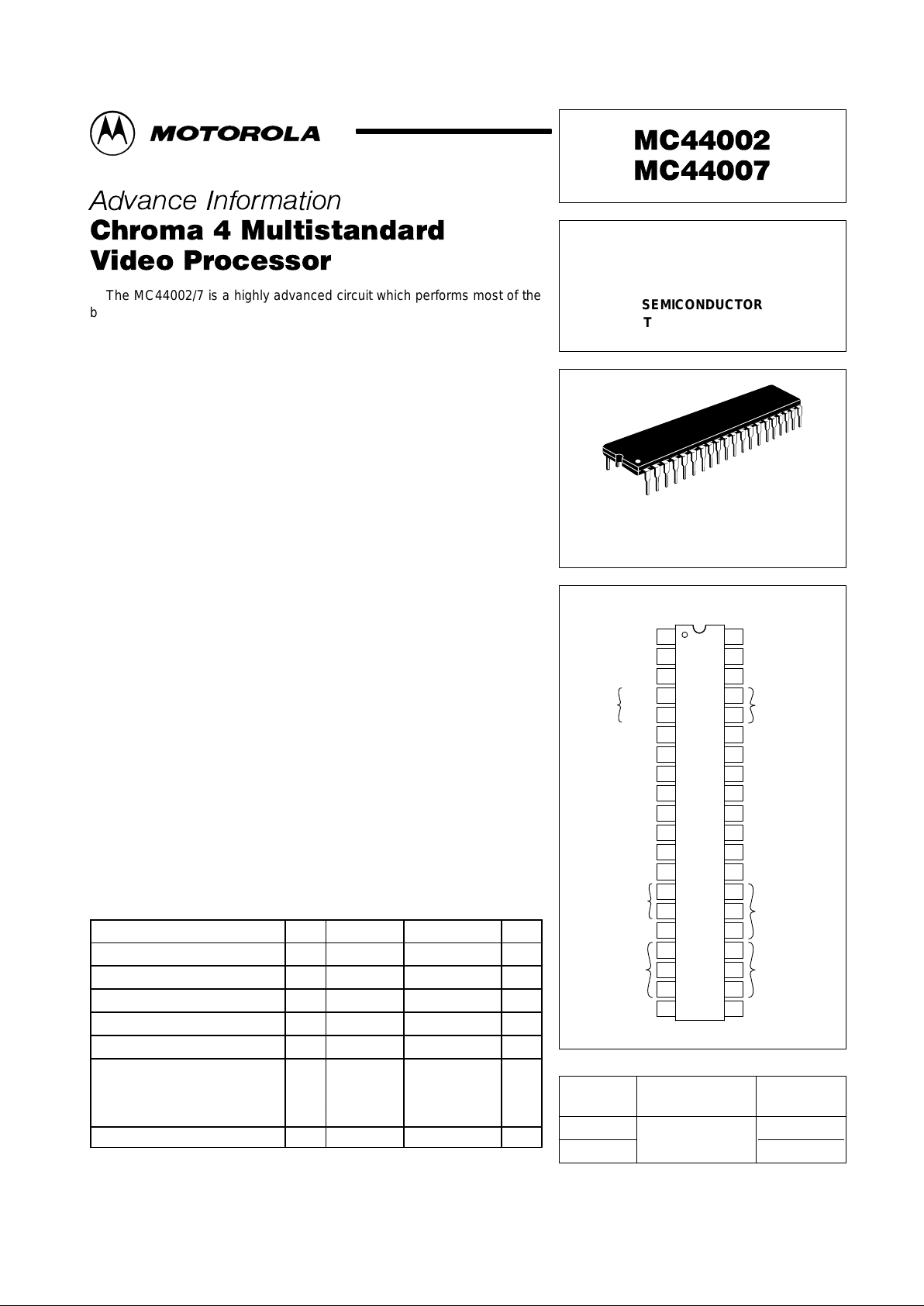
PIN CONNECTIONS
Order this document by MC44002/D
38
40
39
37
36
35
34
33
32
31
30
29
28
27
26
25
24
23
22
21
9
10
11
12
13
14
15
16
17
18
19
20
1
2
3
4
5
6
7
8
(Top View)
ACC
Video 2
I
ref
Clock
Data
V-Ramp
V-Drive
E-W Drive
Osc Loop Filter
Ident
R-Y
B-Y
V
CC
Gnd
(17.7 MHz)
I
Anode
Analog Contrast
SECAM Cal Loop
H-Drive
H-Flyback Input
2
1
(14.3 MHz)
Sandcastle
System Select
Y1 Output
Y1 Clamp
R-Y
B-Y
Signal Gnd
R
G
B
Feedback
Y2
R
G
B
Fast Commutate
Outputs
H-Loop Filter
Inputs
Inputs
Crystals
Outputs
Video 1 In
I2C
MC44007P Plastic DIP
1
MOTOROLA ANALOG IC DEVICE DATA
The MC44002/7 is a highly advanced circuit which performs most of the
basic functions required for a color TV . All of its advanced features are under
processor control via an I2C bus, enabling potentiometer controls to be
removed completely. In this way the component count may be reduced
dramatically , allowing significant cost savings together with the possibility of
implementing sophisticated automatic test routines. Using the MC44002/7,
TV manufacturers will be able to build a standard chassis for anywhere in the
world. Additional features include 4 selectable matrix modes (primarily for
NTSC), fast beam current limiting and 16:9 display.
• Operation from a Single 5.0 V Supply; Typical Current Consumption
Only 120 mA
• Full P AL/SECAM/NTSC Capability (4 Matrix Modes)
• Dual Composite Video or S-VHS Inputs
• All Chroma/Luma Channel Filtering, and Luma Delay Line Are
Integrated Using Sampled Data Filters Requiring No External
Components
• Filters Automatically Commutate with Change of Standard
• Chroma Delay Line is Realized with a 16 Pin Companion Device, the
MC44140
• RGB Drives Incorporate Contrast and Brightness Controls and Auto
Gray Scale
• Switched RGB Inputs with Separate Saturation Control
• Auxiliary Y, R-Y, B-Y Inputs
• Line Timebase Featuring H-Phase Control, T ime Constant and
Switchable Phase Detector Gain
• Vertical Timebase Incorporating Vertical Geometry Corrections
• 16:9 Display Mode Capability
• E-W Parabola Drive Incorporating Horizontal Geometry Corrections
• Beam Current Monitor with Breathing Compensation
• Analog Contrast Control, Allowing Fast Beam Current Limitation
• MC44007 Decoders P AL/NTSC Only
MAXIMUM RATINGS
(TA = 25°C, unless otherwise noted.)
Rating
Pin Symbol Value Unit
Supply Voltage 35 V
CC
6.0 Vdc
Operating Ambient Temperature – T
A
0 to + 70 °C
Storage Temperature – T
stg
– 65 to +150 °C
Junction Temperature – T
J
+150 °C
Drive Output Sink Current 12 I
12
2.0 mA
Applied Voltage Range: Vdc
Feedback 20 V
20
0 to +8.0
Anode Current 9 V
9
– 2.0 to V
CC
All Other Pins – V
i
0 to V
CC
ESD V
NOTE: ESD data available upon request.
This document contains information on a new product. Specifications and information herein
are subject to change without notice.
Motorola, Inc. 1996 Rev 1
MC44002 MC44007
2
MOTOROLA ANALOG IC DEVICE DATA
MAXIMUM RATINGS
(TA = 25°C, unless otherwise noted.)
Rating UnitValueSymbolPin
Human Body Model – – ±2000
Machine Model – – ±200
NOTE: ESD data available upon request.
Chroma
T ake–Of f
Filter
Matrix
Switching
&
RGB Sat
Control
Luma
Select
17.7 MHz
Video 1
(S-VHS)
Video 2
Y2
R-Y
B-Y
Fast Comm.
Filter
Filter
System
Select
Sat &
Hue
System
R-Y B-Y Y1
Memory/Control Registers
Y1
Clamp
Parab
Gen
Beam
Current
Monitor
Control
Loops
Rx/Tx
Red
Green
Blue
Red
Green
Blue
RGB
Outputs
Analog
Contrast
FdbckDataClk
Anode
Current
E-W
Drive
Freq
Divider
Flyback
Sense
14.3 MHz
Loop
2
H Flyback
Pulse
H Drive
5.0 V
V Drive
5.0 V
I
ref
V
Sync
PAL/
NTSC/
SECAM
Decoder
Ident
Clk
Vert
Sync
Sep
Osc
PLL 1
Ramp
Gen
Luma Delay
Peaking & Trap
ACC
SandCastle
Sync
Sep
Input
Select
240
31
13038 37 36 29
14
15
39
32
33
25
27
26
28
21
24
22
17
18
19
16
10
205498637131235
34
23
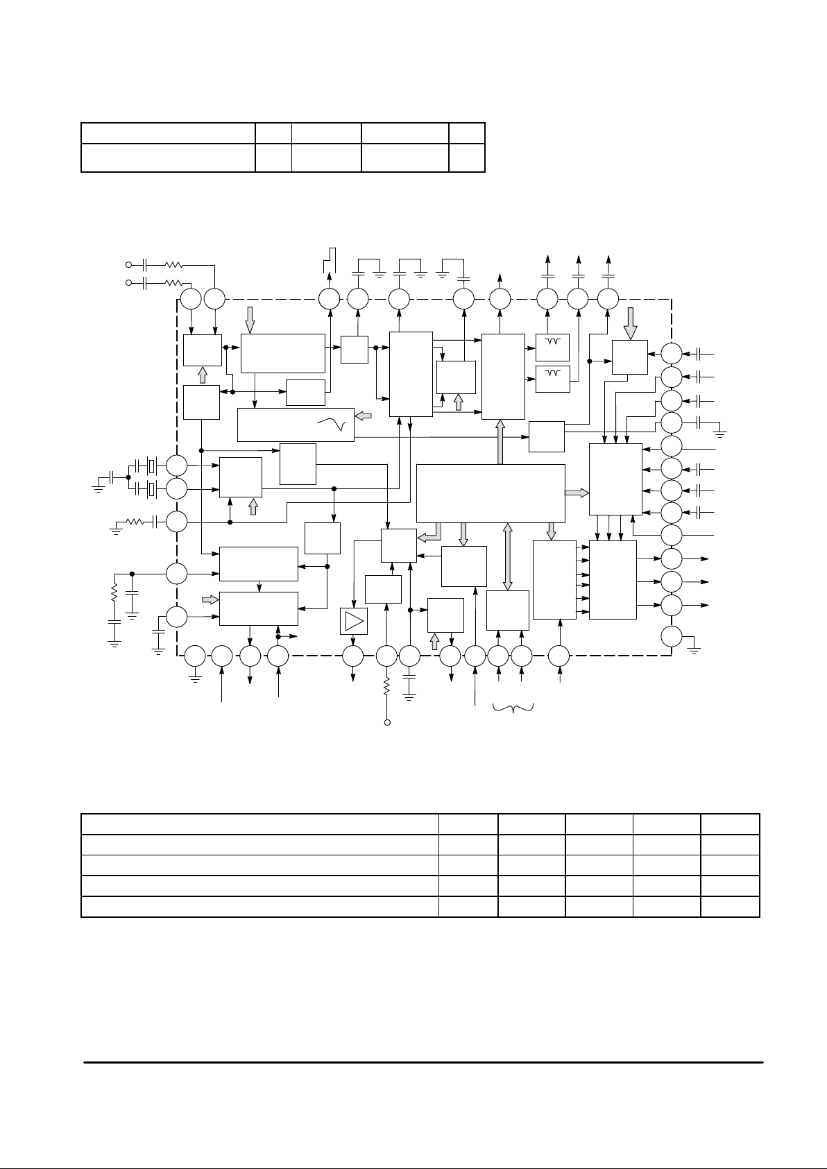
Simplified Block Diagram
11
I2C
Bus
This device contains 6,245 active transistors.
ELECTRICAL CHARACTERISTICS (V
CC
= 5.0 Vdc, I3 = 70 µA, TA = 25°C, unless otherwise noted.)
Characteristic
Pin Min Typ Max Unit
Supply Voltage 35 4.75 5.0 5.25 V
Operating Current 35 90 120 180 mA
Reference Current, Input Voltage 3 1.0 1.3 1.6 V
Thermal Resistance, Junction–to–Ambient – – 56 – °C/W
NOTES: Composite Video Input Signal Level = 1.0 Vpp Horizontal Timebase started (subaddress 00)
Black-to-White = 0.Vpp7 , Syn-to-Black = 0.3 Vpp Vertical Breathing control set to 00; V9 = 0 V
PAL/NTSC = 75% color bars; Burst = 300 mVpp All other analog controls set to midrange 32
SECAM = 75% color bars Video Peaking “P1, P2, P3” bits high

MC44002 MC44007
3
MOTOROLA ANALOG IC DEVICE DATA
TEST CONDITIONS (unless otherwise noted.)
VCC = 5.0 V
I
ref
= 70 µA
TA = 25°C
Video Composite Input = 1.0 Vpp
– Black–to–White = 0.7 Vpp
– Black–to–Sync = 0.3 Vpp
Horizontal Timebase Started (Reg. 00)
Vertical Breathing Control Set to 00
Pin 9 = 0 V
Pin 10 = 5.0 V
PAL/NTSC = 75% Color Bars
–Burst = 300 mVpp
SECAM = 75% Color Bars (MC44002 only)
All Analog Controls Set to Midpoint (32)
Luma Peaking at Min. (P1 – P3 = 111)
Control Bits Setup
Name Value Function Status
V1/V2 1 Video Input 1 Selected
H EN 0 Horizontal Drive Enabled
BRI EN 1 “Bright” Sample “On”
HGAIN1 0 Horizontal Phase Detector Gain Reduced by 3 Enabled
YX EN 0 Luma Matrix Disabled
Y1 EN 1 Luma from Filters “On”
D EN 0 RGB Inputs Enabled
XS 0 Pin 33 Crystal Enabled
TEST 1 Outputs Sampled Once/Field
FSI 0 50 Hz Field Rate
T3 1 Low Pass Filter Enabled
VD1 1 4:3 Display Mode
2xFh 0 Horizontal Drive at 1xFh
NORM 0 Horizontal Reference Divider for 17.7 MHz
HGAIN2 1 Horizontal Phase Detector Gain Reduced by 2 Enabled
INTSEL 1 Long Vertical Time Constant
Y2 EN 0 External Luma Input “Off”
SSD 0 SECAM Mode Select Enabled
CALKIL 1 Horizontal Calibration Loop Enabled
BAI 1 Vertical Blanking for 625 Lines
S–VHS 1 Composite Video Input

MC44002 MC44007
4
MOTOROLA ANALOG IC DEVICE DATA
ELECTRICAL CHARACTERISTICS
Parameter Symbol Pin Min Typ Max Unit
BUS REQUIREMENTS
Maximum Output Low Voltage V
OL(max)
5 – 0.7 – V
I
sink
= 1.0 mA, Device in “Read” Mode
Maximum Sink Current I
sink(max)
5 – 1.0 – mA
VOL = 0.7 V , Device in “Read” Mode
Minimum Input High Voltage V
IH(min)
5 – 3.0 – V
Maximum Input Low Voltage V
IL(max)
5 – 1.5 – V
Maximum Rise Time t
r(max)
4, 5 – 1.0 – µs
Between VIH and VIL Levels
SCL Clock Frequency f
SCL
4 – – 100 kHz
HORIZONTAL TIMEBASE
Free–Running Frequency (Calibration Mode) – 31 kHz
17.734475 MHz Crystal. “NORM” Bit = 0;
“H EN” Bit = 1 (Horizontal Drive Disabled)
15.39 15.625 15.85
14.31818 MHz Crystal. “NORM” Bit = 1;
“H EN” Bit = 1 (Horizontal Drive Disabled)
15.42 15.75 15.98
H–Loop 1 (Pin 15 Current Forced to ± 20 µA) – 12 kHz
Minimum Frequency 13.85 14.25 14.65
Maximum Frequency 16.05 16.55 17.05
Frequency Range – 2.3 –
VCO Control Gain – 12, 15 1.9 2.4 2.9 kHz/V
Phase Detector Gain – 15 18 27 39 µA/µs
“HGAIN1” Bit = 1; “HGAIN2” Bit = 0
Phase Detector Gain Reduction Factor – 15 –
“HGAIN1“ Bit Switched from 1 to 0 2.5 3.0 3.5
“HGAIN2“ Bit Switched from 0 to 1 1.75 2.0 2.25
Line Drive Output Saturation Voltage – 12 – 0.25 0.5 V
I12 = 1.0 mA
Horizontal Drive Pulse Low – 12 – 27 – µs
Defined by Internal Counter, Deflection Transistor
“Off”, Period is 64 µs
Horizontal Flyback Input Resistance – 13 – 50 – kΩ
V13 = 2.0 V
Horizontal Flyback Clamping Voltages – 13 V
I13 = 500 µA – 5.7 –
I13 = –50 µA – –0.5 –
Horizontal Flyback Threshold Current – 13 30 – – µA
Should be Externally Limited to 500 µA Peak by an
External Resistor
Horizontal Phase Control Range – 12 8.0 – 12 µs
Flyback Duration: 12 µs
External Delay Compensation – 12, 13 6.0 – 18 µs
From Horizontal Drive to Center of Flyback Pulse.
Flyback Duration: 12 µs
VERTICAL TIMEBASE (All Values are Related to Pin 3 Reference Current)
Vertical Drive Amplitude (4:3 Display) – 7 V
(00) 1.15 1.33 1.5
(32) 1.55 1.75 1.95
(63) 1.95 2.18 2.4
C6 = 82 nF, Assuming Zero Tolerance
Capacitance, “VDI” Set to “1”
Vertical Drive Amplitude Control Range (4:3 Display) – 7 0.75 0.85 1.0 V
C6 = 82 nF, Assuming Zero Tolerance Capacitance,
“VDI” Set to “1”, Vertical Amplitude Varied from
(00) to (63)

MC44002 MC44007
5
MOTOROLA ANALOG IC DEVICE DATA
ELECTRICAL CHARACTERISTICS (continued)
Parameter UnitMaxTypMinPinSymbol
VERTICAL TIMEBASE (All Values are Related to Pin 3 Reference Current)
Ramp Amplitude Ratio Between 4:3 and 16:9 Display
Modes
– 7 0.7 0.8 0.9 –
Vertical Amplitude = (32)
Maximum Ramp Amplitude Change With 525/625
Mode Change
– 7 – 2.0 – %
Vertical Ramp Low Voltage (4:3 Display) – 7 – 0.65 – V
Pin 6 Voltage Set to 0 V, “VDI” Set to “1”, Vertical
Position = (00)
Vertical Ramp Low Voltage (16:9 Display) – 7 – 0.85 – V
Pin 6 Voltage Set to 0 V, “VDI” Set to “0”, Vertical
Position = (00), Measured After 16:9 Holding
Period
Vertical Ramp High Voltage – 7 – 4.15 – V
Pin 6 Open, “VDI” Set to “0” or “1”, Vertical
Position = (63)
Vertical Ramp Position Control Range – 7 ±0.5 ±0.75 ±1.0 V
Versus Vertical Ramp Voltage at Vertical Position
(32), Measured at Vm, “VDI” Set to “0” or “1”,
Vertical Position Varied from (00) to (63)
Vertical Ramp Clamping Duration (tc) – 7 – 512 – µs
Defined by Internal Counter
Maximum Output Source Current – 7 1.0 – – mA
Maximum Output Sink Current – 7 200 – – µA
Vertical Linearity – 7 –
(00) – 0.8 –
(63) – 1.1 –
Change in Ramp current as Pin 9 Current Varied from
0 to 6.4 µA
– 6 µA
Vertical Breathing Correction = (63) 0.15 0.75 1.3
Vertical Breathing Correction = (00) – 0 –
Gain V7/V6 – 6, 7 0.9 0.95 1.0 V/V
E–W CORRECTION (V6(b) = 0.2 V , V6(m) = 1.1 V, V6(e) = 2.0 V)
Horizontal Amplitude – 8 µA
(00) 0 0.2 20
(63) 150 300 –
Corner Correction = (00), Tilt = (32), Parabola
Amplitude = (00), Measured at Tm.
Parabola Amplitude – 8 µA
(00) 0 0.2 10
(63) 100 250 –
Corner Correction = (00), Horizontal Amplitude =
(32), Tilt = (32), Measured at Tb, Tm and T
e.
Corner Correction – 8 µA
(00) 0 0.2 10
(63) – –150 –30
Horizontal Amplitude = (63), Parabola Amplitude =
(00), Tilt = (32), Measured at Tb, Tm and Te.
Parabola Tilt – 8 –
(00) – 1.9 –
(63) – –1.9 –
Corner Correction = (00), Horizontal Amplitude =
(32), Parabola Amplitude = (32), Measured at Tb,
Tm and Te.
E–W Drive Output Voltage – 8 1.0 – V
CC
V

MC44002 MC44007
6
MOTOROLA ANALOG IC DEVICE DATA
ELECTRICAL CHARACTERISTICS (continued)
Parameter UnitMaxTypMinPinSymbol
E–W CORRECTION (V6(b) = 0.2 V, V6(m) = 1.1 V, V6(e) = 2.0 V)
E–W DACs Differential Non–Linearity Error – 8 LSB
At Minor Transitions: Steps 0–1: 1–2; 3–4; 7–8;
15–16.
–1.0 – 1.0
At Major Transition: Step 31–32 –2.0 – 1.0
SYNC SEPARATOR
Sync Amplitude to Operate the Device – 2, 40 100 – – mV
From Black to Sync, Black Picture, Standard Timing
Specifications on Sync Signal
22, 23,
24, 25
– 160 –
Vertical Sync Separator Delay T ime: t
d
– 2, 40 µs
“INTSEL” = 0 – 36 –
“INTSEL” = 1 – 68 –
From Vertical Sync Pulse to Vertical Ramp Reset
Vertical Sync Window – 2, 40,
22, 23,
24, 25
448 – 740 Half
Lines
COMPOSITE VIDEO PROCESSING (All measurements in NORMAL mode, unless otherwise noted.)
Composite Video Input Amplitude – 2, 40 0.7 1.0 1.4 Vpp
Load Impedance 75 Ω, Less than 5% Distortion
Video 1/Video 2 Input Crosstalk – 29 – – –40 dB
@ f = (2.0 MHz), Measured on Y1 Output
Variable Input LPF Cut–Of f Frequency – 29 MHz
17.7 MHz Crystal Selected – 6.0 –
14.3 MHz Crystal Selected – 4.85 –
Chroma Subcarrier Rejection – 29 dB
PAL 4.43 MHz (17.7 MHz Crystal Selected) 25 30 –
NTSC 3.58 MHz (14.3 MHz Crystal Selected) 25 30 –
SECAM (FoR and FoB) (17.7 MHz Crystal Selected) 18 20 –
Y1 Output Resistance – 29 – – 300 Ω
Y1 Bandwidth (–3.0 dB) – 29 MHz
PAL
Minimum Peaking, “T3” Set to 1 (Input LPF “On”)
2.5 3.0 –
SECAM
Minimum Peaking, “T3” Set to 0 (Input LPF “Off”)
2.5 3.0 –
Luma Peaking Range – 29 6.0 8.5 – dB
Measured at 3.0 MHz, 17.7 MHz Crystal Selected
Luma Gain (@ 100 kHz) – 2, 40, 29 0.9 1.1 1.3 V/V
Overshoot – 29 – 5.0 – %
Peaking at Step 3 (100)
Source Impedance – 2, 40 0 – 1.5 kΩ
Luma Delay Range – 29 ns
PAL/SECAM (17.7 MHz Crystal Selected) – 280 –
NTSC 3.58 (14.3 MHz Crystal Selected) – 350 –
Video In to Luma Out Delay Difference Between PAL
and SECAM (MC44002 only)
– 29, 40 – 260 – ns
Luma Delay Minimum: (D1 D2 D3) = (0 0 0), Green
to Magenta Transition, “T3” Set to 1 in PAL, to 0 in
SECAM
PAL/NTSC DECODER
Chroma Output Variation – 36, 37 – – 3.0 dB
For a Burst Input Varied from 60 mV to 600 mV
Color Kill Attenuation – 36, 37 40 – – dB
Referred to Standard Color Video Input,
Monochrome Mode Selected

MC44002 MC44007
7
MOTOROLA ANALOG IC DEVICE DATA
ELECTRICAL CHARACTERISTICS (continued)
Parameter UnitMaxTypMinPinSymbol
PAL/NTSC DECODER
Color Difference Output Distortion – 36, 37 – – 5.0 %
@ 1.5 V Output Signal
Residual Chroma Subcarrier Rejection – 36, 37 dB
PAL 40 – –
NTSC 40 – –
Referred to Video Input
Oscillator Pull–In Range – 32, 33 Hz
PAL ±350 – –
NTSC ±400 – –
Referred to Nominal Subcarrier Frequency, with
Ideal Xtal
R–Y, B–Y Channel Separation – 36, 37 30 – – dB
B–Y/R–Y Amplitude Ratio – 36, 37 – 1.3 – V/V
At Standard Color Bars Signal
B–Y/R–Y Amplitude Ratio Spread – 36, 37 –2.0 – 2.0 dB
At Standard Color Bars Signal
Minimum Burst Level for “ACC Active” Flag “On” – 2, 40 – 10 20 mVpp
Standard Set to PAL or NTSC, Increasing Burst
Level Steps
Minimum Burst Level for “PAL Identified” Flag “On” – 2, 40 – 5.0 20 mVpp
Standard Set to PAL or NTSC, Increasing Burst
Level Steps
Maximum Burst Level for “ACC Active” Flag “Off” – 2, 40 – 5.0 – mVpp
Standard Set to PAL or NTSC, Decreasing Burst
Level Steps
Maximum Burst Level for “PAL Identified” Flag “Of f” – 2, 40 – 1.0 – mVpp
Standard Set to PAL or NTSC, Decreasing Burst
Level Steps
(B–Y) Color Difference Output Levels – 36 0.7 1.1 1.5 V
Relative to 75% Color Bars
Hue DAC Control Range – 36, 37 ±20 – – Deg
Hue Control Register Varying from (00) to (63)
Chroma to Luma Delay – 29, 36 ns
PAL – 80 –
NTSC – 100 –
Measured on (B–Y) Output, Luma Delay Set to
Minimum: (D1 D2 D3) = (0 0 0), Green to Magenta
Transition, “T3” Set to 1
DELAY LINE CONTROL SIGNALS
System Select – 30
PAL – 75 400 mV
NTSC 1.4 1.65 1.9 V
SECAM (MC44002 only) 2.75 3.0 3.25 V
EXTERNAL 3.7 4.0 4.3 V
Sandcastle – 31
Level 1 3.7 4.0 4.3 V
Level 2 2.75 2.95 3.15 V
Level 3 1..3 1.55 1.8 V
Level 4 – 75 – mV
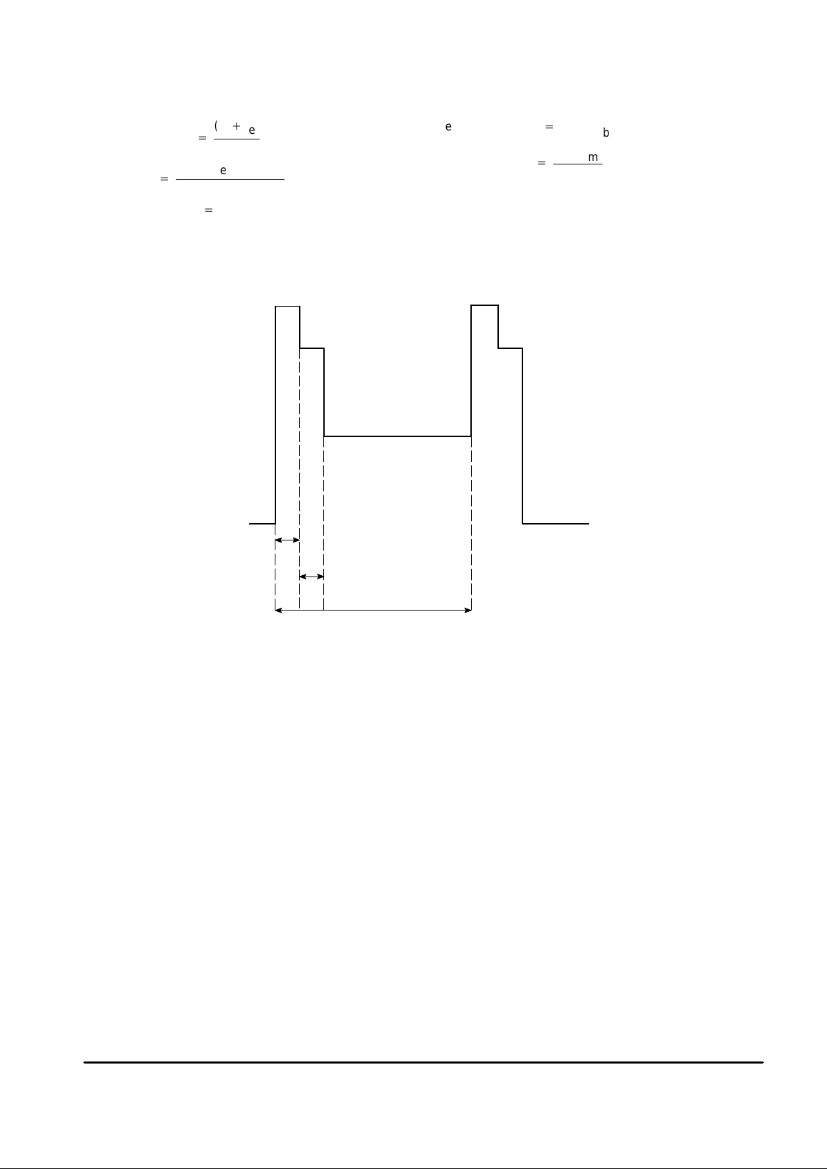
See Figure 4
Sandcastle – 31 µs
t1 5.0 6.0 7.0
t2 4.0 5.0 6.0
See Figure 4, Values Defined by Internal Counter

MC44002 MC44007
8
MOTOROLA ANALOG IC DEVICE DATA
ELECTRICAL CHARACTERISTICS (continued)
Parameter UnitMaxTypMinPinSymbol
S–VHS VIDEO PROCESSING (S–VHS Set to 0, “T3” Set to 0)
Y1 Bandwidth – 29 3.2 3.5 – MHz
Luma Peaking Set to Minimum
Minimum Burst Level for “ACC Active” Flag “On” – 2, 40 – 10 20 mVpp
Standard Set to PAL or NTSC, Increasing Burst
Level Steps
Minimum Burst Level for “PAL Identified” Flag “On” – 2, 40 – 5.0 20 mVpp
Standard Set to PAL or NTSC, Increasing Burst
Level Steps
Maximum Burst Level for “ACC Active” Flag “Off” – 2, 40 – 5.0 – mVpp
Standard Set to PAL or NTSC, Decreasing Burst
Level Steps
Maximum Burst Level for “PAL Identified” Flag “Of f” – 2, 40 – 1.0 – mVpp
Standard Set to PAL or NTSC, Decreasing Burst
Level Steps
Video In to Luma Out Delay Difference Between
S–VHS and Normal Mode
– 2, 40, 29 – 310 – ns
Luma Delay Minimum in Normal Mode, Set to Step
6 in S–VHS Mode, Green to Magenta Transition,
“T3” Set to 1 in Normal Mode, to 0 in S–VHS Mode
Chroma to Luma Delay Difference Between S–VHS
and Normal Mode
– 29, 36,
2, 40
– 60 – ns
Measured on (B–Y) Output, Luma Delay Minimum
in Normal Mode, Set to Step 6 in S–VHS Mode,
Green to Magenta Transition, “T3” Set to 1 in
Normal Mode, to 0 in S–VHS Mode
SECAM DECODER (MC44002 ONL Y)
Minimum Subcarrier Level for “SECAM Identified”
Flag
– 2, 40 – 10 20 mVpp
Measured at foR
Color Kill Attenuation – 36, 37 40 50 – dB
Monochrome Mode Selected Referred to Color
Difference Output Signal with SECAM Selected
and Identified
Color Difference Zero Level Error – 36, 37 – ±1.0 ±3.0 %
Relative to 75% Color Bars, Difference Between
Signal Measured at t1 and Active Black Level
(Black Bar)
Color Difference Output Distortion – 36, 37 – – 5.0 %
Subcarrier Level at foR = 20–400 mV @ 1.5 V
Output Signal
Transient Response – ns
(B–Y) 36 – 650 800
(R–Y) 37 – 750 900
Generator Rise Time – 600 ns (B–Y), Green to
Magenta Transition, Measured Between 10% and
90% Levels
B–Y/R–Y Amplitude – 36, 37
Ratio – 1.3 – V/V
Ratio Spread –2.0 – 2.0 dB
Relative to 75% Color Bars
Residual Carrier and Harmonics (4.0 to 13.5 MHz) – 36, 37 – – 1.0 %
At Standard Color Bars Signal
(B–Y) Color Difference Output Levels – 36 – 1.1 – V
Relative to 75% Color Bars
PAL/SECAM Color Dif ference Ratio – 36 0.8 1.0 1.2 –
Nominal Input Signals

MC44002 MC44007
9
MOTOROLA ANALOG IC DEVICE DATA
ELECTRICAL CHARACTERISTICS (continued)
Parameter UnitMaxTypMinPinSymbol
SECAM DECODER (MC44002 ONL Y)
Chroma to Luma Delay – 29, 36 – 420 – ns
Luma Delay Set to Minimum: (D1 D2 D3) = (0 0 0),
Green to Magenta Transition, “T3” Set to 0
Patterning – 36 – – 5.0 %
Full Screen 75% Color Frequency, 500 kHz Low
Pass Filter, Relative to Black to Color Output Signal
Line to Line Luma Levels Difference – 29 – – 1.5 %
Full Screen 75% Y ellow Color Frequency, Relative
to Black to Yellow Output Signal
Chroma to Luma Delay Difference Between P AL and
SECAM
– 29, 36 – 340 – ns
Measured on (B–Y) Output, Luma Delay Set to
Minimum: (D1 D2 D3) = (0 0 0), Green to Magenta
Transition, “T3” Set to 0 in SECAM, to 1 in PAL
COLOR DIFFERENCE STAGES
RGB Input Amplitude – 22, 23, 500 700 1000 mVpp
Black to Peak (Less than 5% Distortion at RGB
Outputs)
24
Fast Commutate – 21 V
Low Level – – 0.5
High Level 1.0 – –
Y2 Input Amplitude – 25 0.7 1.0 1.4 Vpp
(Less than 5% Distortion at RGB Outputs)
Color Difference Input Amplitude – 26, 27 – – 1.8 Vpp
(Less than 5% Distortion at RGB Outputs)
Y2/Y1 Crosstalk – 25, 29 – –40 –30 dB
Measured at RGB Outputs, Measured at f = (2.0 MHz)
RGB to Y Crosstalk – 22, 23, – –40 –30 dB
Measured at RGB Outputs, Measured at f = (2.0 MHz) 24, 25,
29
RGB Transconductance Bandwidth (@ –1.0 dB) – 24, 17,
23, 18,
22, 19
6.5 – – MHz
Gain Reduction in ACL Mode – 10, 17, – 12.5 – dB
Pin 10 Voltage Varying from 0 to 5.0 v 18, 19
Gain Reduction Sensitivity in ACL Mode – 10, 17, – 20 – dB/V
Pin 10 Voltage Varying from 2.0 to 2.5 V 18, 19
Demodulation Angles and Amplitudes – – Deg
Mode A Rm – 0.562 –
Ra – 90 –
Gm – 0.344 –
Ga – 237 –
Mode B Rm – 0.9 –
Ra – 100 –
Gm – 0.3 –
Ga – 236 –
Mode C Rm – 0.9 –
Ra – 106 –
Gm – 0.3 –
Ga – 240 –
Mode D Rm – 0.91 –
Ra – 106 –
Gm – 0.31 –
Ga – 246 –
Definitions: Rm/Gm = Module, Ra/Ga = Argument
MC44002 MC44007
10
MOTOROLA ANALOG IC DEVICE DATA
ELECTRICAL CHARACTERISTICS (continued)
Parameter UnitMaxTypMinPinSymbol
RGB OUTPUT STAGES
Low Dark Sample Output Current – 17, 18, mA
Red 19 – – 3.15
Green – – 3.15
Blue – – 3.15
Dark Sample Cathode Current 5.0 to 15 µA, DC
DAC Set to Full Scale, See Figure 1
High Dark Sample Output Current – 17, 18, mA
Red 19 3.95 – –
Green 3.95 – –
Blue 3.95 – –
Dark Sample Cathode Current 5.0 to 15 µA, DC
DAC Set to Zero, See Figure 1
Blanking Output Current – 17, 18,
19
6.0 – – mA
Maximum Y to RGB Output Transconductance – 17, 18, 6.0 7.0 8.0 mA/V
Gain DAC Set to Full Scale 19
Brightness – – V
(00) – 30 –
(63) – –20 –
Wrt Dark Sample Cathode Voltage,
High Voltage Output Stage T ransimpedance
39 kΩ, Dark Sample Cathode Current 15 µA, Dark
Sample Cathode Voltage 140 V
RGB Dark Sample Current Intensity Range – 20 15 20 – dB
RGB Intensity DACs Varying from (00) to (63)
Bright to Dark Sample Current Ratio – 20 8.0 9.5 11 µA/µA
Leakage Loop – 20 µA
Sink Current 20 – –
Source Current 5.0 – –
Average Beam Current Detection Level – 9 V
Excess Flag 0.9 1.0 1.1
Overload Flag –1.3 –1.2 –1.1
Peak Beam Current Detection Level – 20 6.5 6.8 7.1 V
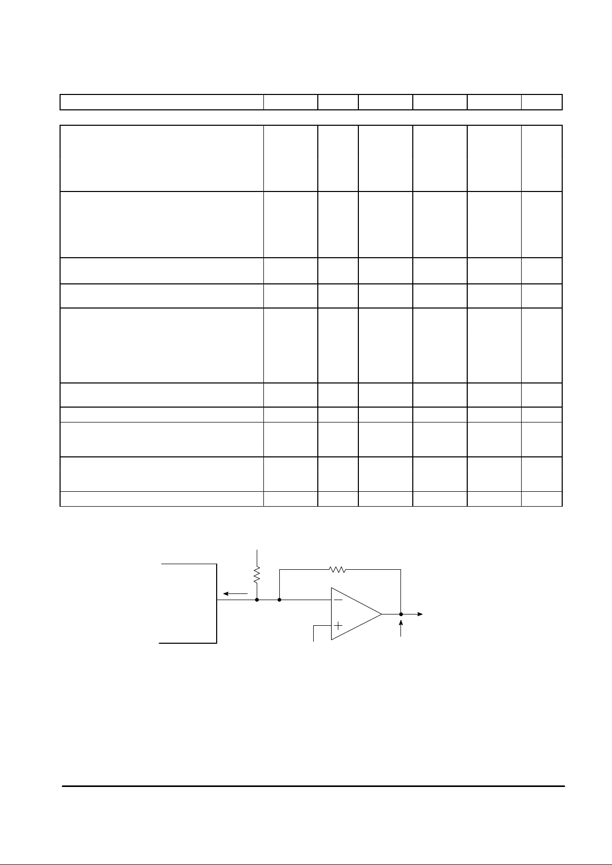
Figure 1. Example of Output Circuitry
Vp, V
ref
, R
FDBK
and Rp values will determine the exact operating point.
For example, let us take:
Vp = 5.0 V R
FDBK
= 39 kΩ
V
ref
= 3.6 V
Rp = 6.8 kΩ
The formula giving the Dark Cathode Voltage with above circuit is: Vdk = V
ref
+ R
FDBK
*(V
ref
– Vp + lodk*Rp) / R
p
With above application, component values and lodk specifications, all 3 cathodes on all devices will always have a range of at least 120 V to 150 V.
By changing the values of Vp, V
ref
and Rp, the cathode voltage range may be shifted up or down as required.
lodk
V
ref
V
dk
Picture Tube
Cathode
R
FDBK
R
P
V
P
Pins 17, 18, 19
MC44002/7P
MC44002 MC44007
11
MOTOROLA ANALOG IC DEVICE DATA
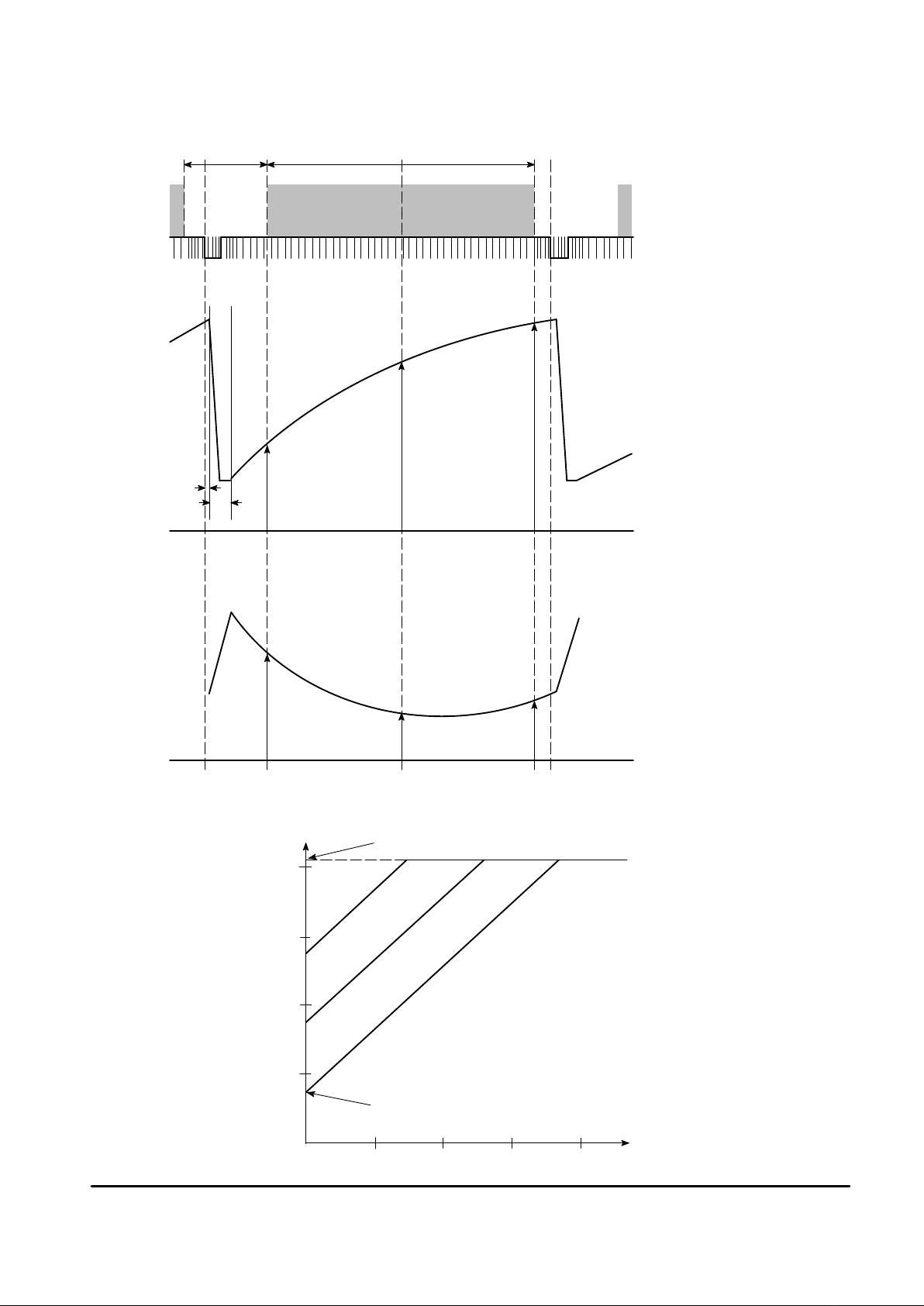
Figure 2. Vertical Waveforms
Figure 3. Vertical Ramp Positions (V7 versus V6)
1.6 ms 18.4 ms
T
b
T
m
T
e
V
b
V
m
V
e
I
b
I
m
I
e
t
d
t
c
Video Signal
Vertical Ramp W aveform
Parabola Waveform
V Ramp High Voltage
V Ramp Low Voltage
(XX) = Values of (80) Register
(63)
Pin 6 Voltage (V)
Pin 7 Voltage (V)
4
1
(32) (00)
3
2
1
234
MC44002 MC44007
12
MOTOROLA ANALOG IC DEVICE DATA
Definitions
Parabola Amplitude
+
(ib)
ie)
2
–i
m
Parabola Tilt
+
(ie–ib)
Parabola Amplitude
Horizontal Amplitude+i
m
Vertical Amplitude+Ve–V
b
Vertical Linearity
+
(Ve–Vm)
Vm–V
b
Corner correction is calculated in the same way as Parabola Amplitude.
Figure 4. Sandcastle Output (Pin 31)
64 µs
1
2
4
3
t1
t2
GENERAL DESCRIPTION OF THE CHROMA 4 SYSTEM
Figure 5 shows a simplified block diagram representation
of the basic system using the MC44002/7 and its companion
device the MC44140 chroma delay line. The MC44002/7 has
been designed to carry out all the processing of video
signals, display controls and timebase functions. There are
two video inputs which can be used for normal composite
video or separate Y and C inputs. In either case, the inputs
are interchangeable and selection is made via the I2C bus.
The video is decoded within the MC44002/7 and involves
separation, filtering, delay of the luminance part of the signal
and demodulation of the chroma into color difference signals.
The luminance (called Y1) together with the demodulated
R-Y and B-Y are all then brought out from the IC. The color
difference signals then enter the MC44140 which performs
color correction in PAL and the delay line function in SECAM.
Corrected color difference signals then re-enter the
MC44002/7.
 Loading...