

Motorola MC34C87D, MC34C87P Datasheet
MC34C87MOTOROLA
1
Product Preview
CMOS
The MC34C87 is a quad differential line driver designed for digital data
transmission over balanced lines. The MC34C87 meets all the requirements of
standard EIA–422–A while retaining the low–power characteristics of CMOS.
The MC34C87 accepts TTL or CMOS input levels and translates these to
EIA–422–A output level. This part uses special output circuitry that enables the
individual drivers to power down without loading down the bus. The MC34C87
also includes special circuitry which will set the outputs to a high impedance
mode during power up or down, preventing spurious glitches. Each enable pin
controls two drivers.
The MC34C87 is pin compatible with the MC3487.
All pins are protected against damage due to electrostatic discharges.
• Maximum Power Supply Current: 3 mA
• 2000 V ESD Protection on the Inputs and the Outputs
• TTL/CMOS Input Compatible
• Typical Propagation Delay: 6 ns
• Typical Output Skew: 1 ns
• Meets VO = 6.0 V (and VO = – 0.25 V), VCC = 0 V, IO < 100 µA
Requirement
• Operation from Single 5 V Supply
• High Impedance Mode for Outputs Connected to System Buses
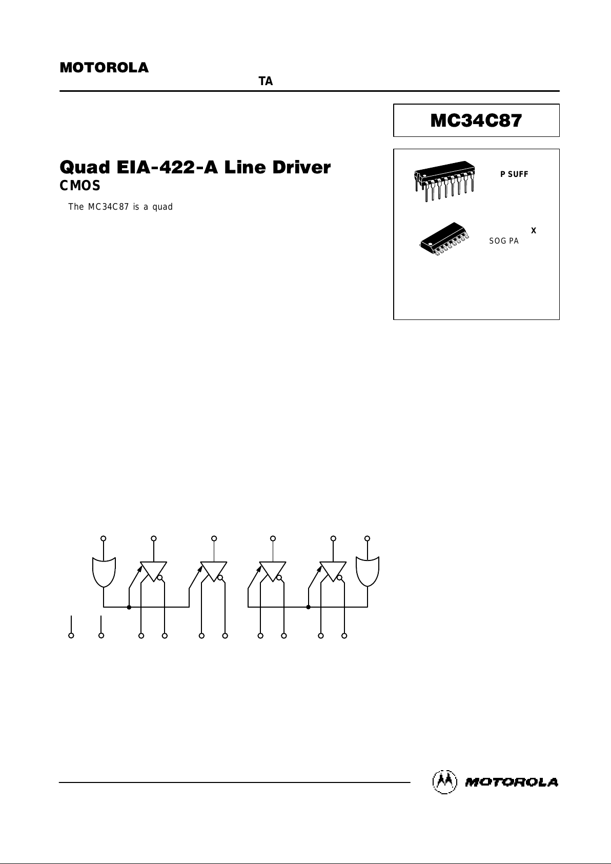
BLOCK DIAGRAM
C/D
CONTROL
INPUT D INPUT C INPUT B INPUT A
OUTPUTD2OUTPUTD1OUTPUTC2OUTPUTC1OUTPUTB2OUTPUTB1OUTPUTA2OUTPUT
A1
V
CC
GND
12
15 9 7 1
8 16 14 13 10 11 6 5 2 3
4
This document contains information on a product under development. Motorola reserves the right to change or discontinue this product without notice.
Order this document
by MC34C87/D
SEMICONDUCTOR TECHNICAL DATA
P SUFFIX
PLASTIC DIP
CASE 648
D SUFFIX
SOG PACKAGE
CASE 751B
ORDERING INFORMATION
MC34C87P Plastic DIP
MC34C87D SOG Package
16
1
16
1
Motorola, Inc. 1995
REV 3
1993
MC34C87 MOTOROLA
2
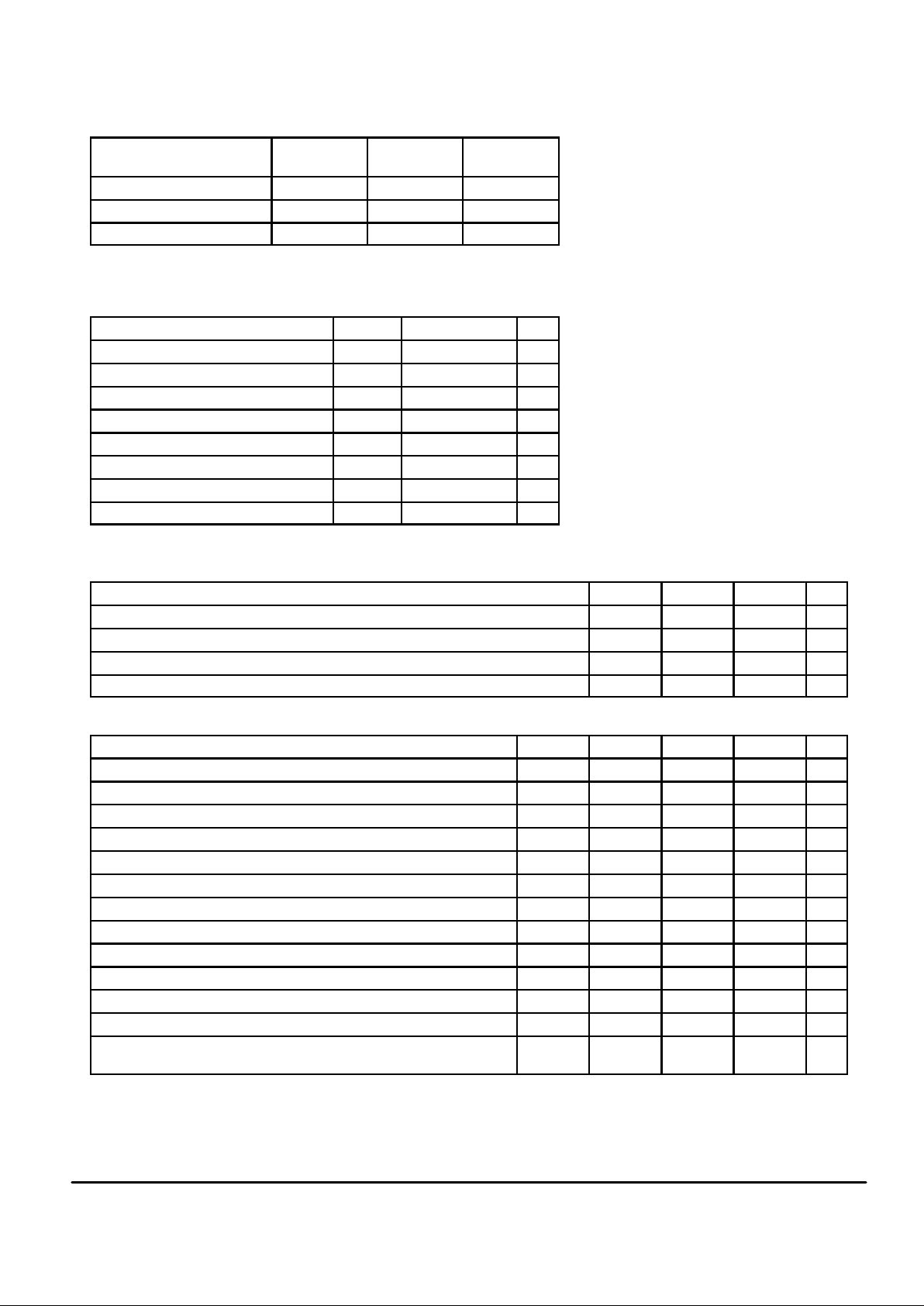
TRUTH TABLE
Control Input Input
Non–Inverting
Output
Inverting
Output
L X Z Z
H H H L
H L L H
X = Don’t Care H = High Logic State
Z = High Impedance L = Low Logic State
MAXIMUM RATINGS
Rating Symbol Value Unit
Power Supply Voltage V
CC
7 V
DC Input Voltage V
in
– 1.5 to VCC + 1.5 V
DC Output Voltage* V
out
– 0.5 to VCC + 0.5 V
DC Output Current, per Pin I
out
150 mA
DC VCC or GND Current, per Pin I
DD
150 mA
Storage Temperature T
stg
– 65 to + 150 °C
Power Dissipation P
D
500 mW
ESD (Human Body Model) 2000 V
*Power–on conditions.
OPERATING CONDITIONS
Rating Symbol Min Max Unit
Power Supply Voltage V
CC
4.5 5.5 V
DC Input Voltage V
in
0 V
CC
V
Operating Temperature Range T
A
– 40 + 85 °C
Input Rise and Fall Time tr, t
f
— 500 ns
DC CHARACTERISTICS (V
CC
= 4.5 to 5.5 V, TA = – 40 to + 85°C, unless otherwise stated)
Parameter
Symbol Min Typ Max Unit
Input Voltage (Low Logic State) V
IL
— — 0.8 V
Input Voltage (High Logic State) V
IH
2.0 — — V
Output Voltage (Low Logic State) I
sink
= 20 mA V
OL
— 0.3 0.5 V
Output Voltage (High Logic State) I
source
= – 20 mA V
OH
2.5 2.8 — V
Output Differential Voltage RL = 100 Ω (Note 1) V
OD
2.0 — — V
Output Differential Voltage Difference RL = 100 Ω (Note 1) D(VOD) — — ± 0.4 V
Output Offset Voltage RL = 100 Ω (Note 1) V
OS
— — 3.0 V
Output Offset Voltage Difference RL = 100 Ω (Note 1) D(VOS) — — ± 0.4 V
Input Current Vin = VCC, GND, VIH or V
IL
I
in
— — ± 1.0 µA
Quiescent Supply Current I
out
= 0 µA I
CC
— — 3.0 mA
Output Short Circuit Current (Note 2) I
OS
– 30 – 100 – 150 mA
Output Leakage Current (High–Z State) V
out
= VCC or GND I
O(Z)
— — ± 1.0 µA
Output Leakage Current (Power Off) V
out
= 6 V
V
out
= – 0.25 V
I
oxh
I
oxl
—
—
—
—
100
– 100
µA
NOTES:
1. See EIA specifications EIA–422–A for exact test conditions.
2. Only one output may be shorted at a time.
This device contains circuitry to protect the
inputs against damage due to high static voltages or electric fields; however, it is advised that
normal precautions be taken to avoid applications of any voltage higher than the maximum
rated voltages to this high impedance circuit.
For proper operation it is recommended that
Vin and V
out
be constrained to the range VSS ≤
(Vin or V
out
) ≤ VDD. Reliability of operation is
enhanced if unused inputs are tied to and
appropriate logic voltage level (e.g., either V
SS
or VDD).
 Loading...