

Motorola MC3488AD, MC3488ADR2, MC3488AP1 Datasheet
The MC3488A dual is single–ended line driver has been designed to
satisfy the requirements of EIA standards EIA–423 and EIA–232D, as well
as CCITT X.26, X.28 and Federal Standard FIDS1030. It is suitable for use
where signal wave shaping is desired and the output load resistance is
greater than 450 ohms. Output slew rates are adjustable from 1.0 µs to
100 µs by a single external resistor. Output level and slew rate are
insensitive to power supply variations. Input undershoot diodes limit
transients below ground and output current limiting is provided in both output
states.
The MC3488A has a standard 1.5 V input logic threshold for TTL or
NMOS compatibility .
• PNP Buffered Inputs to Minimize Input Loading
• Short Circuit Protection
• Adjustable Slew Rate Limiting
• MC3488A Equivalent to 9636A
• Output Levels and Slew Rates are Insensitive to Power
Supply Voltages
• No External Blocking Diode Required for V
• Second Source µA9636A
EE
Supply
Order this document by MC3488A/D
DUAL
EIA–423/EIA–232D
DRIVER
SEMICONDUCTOR
TECHNICAL DATA
P1 SUFFIX
PLASTIC PACKAGE
CASE 626
D SUFFIX
PLASTIC PACKAGE
CASE 751
(SO–8)
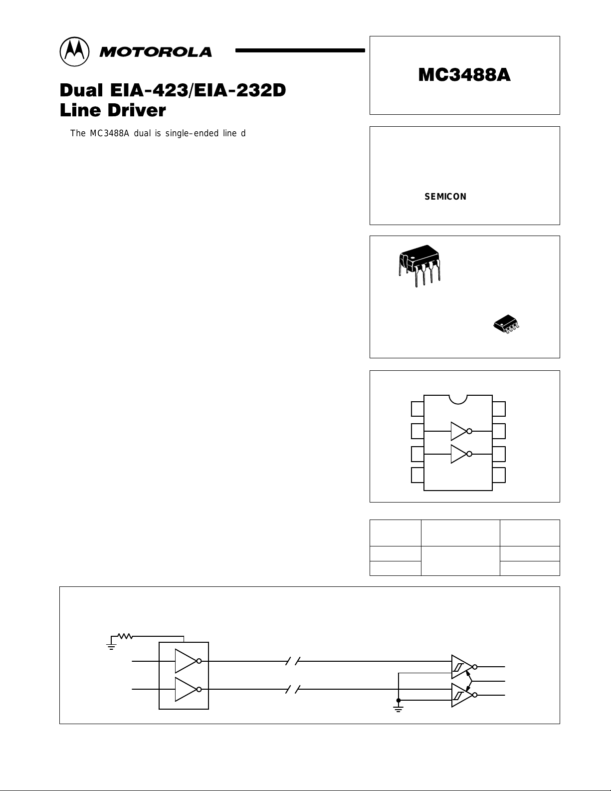
Wave Shape
Control
Simplified Application
MC3488A Driver
RS–423 Interface
Wave
Shape
Input A
Input B
Gnd
ORDERING INFORMATION
Device
MC3488AP1
MC3488AD
PIN CONNECTIONS
1
2
3
4
Operating
Temperature Range
TA = 0 to +70°C
MC3486
Three–State Receiver
V
8
CC
7
Output A
6
Output B
5
V
EE
Plastic DIP
Package
SO–8
TTL Logic
MOTOROLA ANALOG IC DEVICE DATA
Motorola, Inc. 1996 Rev 2
1
MC3488A
MAXIMUM RATINGS (Note 1)
Rating Symbol Value Unit
Power Supply Voltages V
Output Current
Source
Sink
Operating Ambient Temperature T
Junction Temperature Range T
Storage Temperature Range T
V
I
O+
I
O–
CC
EE
A
J
stg
RECOMMENDED OPERATING CONDITIONS
Characteristic Symbol Min Typ Max Unit
Power Supply Voltages V
Operating Temperature Range T
Wave Shaping Resistor R
TARGET ELECTRICAL CHARACTERISTICS (Unless otherwise noted, specifications apply over recommended operating conditions)
Characteristic
Input Voltage – Low Logic State V
Input Voltage – High Logic State V
Input Current – Low Logic State
(VIL = 0.4 V)
Input Current – High Logic State
(VIH = 2.4 V)
(VIH = 5.5 V)
Input Clamp Diode Voltage
(IIK = – 15 mA)
Output Voltage – Low Logic State
(RL = ∞) EIA–423
(RL= 3.0 kΩ) EIA–232D
(RL= 450 Ω) EIA–423
Output Voltage – High Logic State
(RL = ∞) EIA–423
(RL.= 3.0 kΩ) EIA–232D
(RL = 450 Ω) EIA–423
Output Resistance
(RL q 450 Ω)
Output Short–Circuit Current (Note 2)
(Vin = V
(Vin = V
Output Leakage Current (Note 3)
(VCC = VEE = 0 V, – 6.0 V p Vop
Power Supply Currents
(RW = 100 kΩ, RL = ∞, VIL p Vinp
NOTES: 1. Devices should not be operated at these values. The IElectrical CharacteristicsI provide conditions for actual device operation.
= 0 V)
out
, V
IH(Min)
2.One output shorted at a time.
3.No VEE diode required.
out
= 0 V)
6.0 V)
VIH)
+ 15
– 15
+ 150
– 150
0 to + 70 °C
150 °C
– 65 to + 150 °C
CC
V
EE
A
WS
10.8
– 13.2
0 25 70 °C
10 – 1000 kΩ
Symbol Min Typ Max Unit
IL
IH
I
IL
I
IH1
I
IH2
V
IK
V
OL
V
OH
R
O
I
OSH
I
OSL
I
ox
I
CC
I
EE
V
mA
12
–12
– – 0.8 V
2.0 – – V
– 80 – – µA
–
–
– 1.5 – – V
– 6.0
– 6.0
– 6.0
5.0
5.0
4.0
– 25 50 Ω
– 150
+15
– 100 – 100 µA
–
–18
–
–
–
–
–
–
–
–
–
–
–
–
13.2
– 10.8
10
100
– 5.0
– 5.0
– 4.0
6.0
6.0
6.0
– 15
+ 150
+ 18
–
V
µA
V
V
mA
mA
2
MOTOROLA ANALOG IC DEVICE DATA
 Loading...