

Motorola MC3487D, MC3487P Datasheet
Device
Operating
Temperature Range
Package
SEMICONDUCTOR
TECHNICAL DATA
QUAD EIA–422 LINE DRIVER
WITH THREE–STATE
OUTPUTS
ORDERING INFORMATION
MC3487P
MC3487D
TA = 0 to +70°C
Plastic DIP
SO–16
PIN CONNECTIONS
Order this document by MC3487/D
P SUFFIX
PLASTIC PACKAGE
CASE 648
D SUFFIX
PLASTIC PACKAGE
CASE 751B
(SO–16)
10
11
13
14
Outputs B
Outputs A
2
3
5
6
Outputs C
Outputs D
V
CC
Input D
C/D Control
Input C98
7
1
4
Gnd
Input B
A/B Control
12
15
16
Input A
1
MOTOROLA ANALOG IC DEVICE DATA
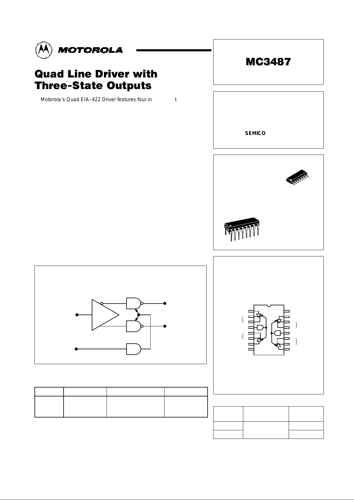
Motorolais Quad EIA–422 Driver features four independent driver chains
which comply with EIA Standards for the Electrical Characteristics of
Balanced Voltage Digital Interface Circuits. The outputs are three–state
structures which are forced to a high impedance state when the appropriate
output control pin reaches a logic zero condition. All input pins are PNP
buffered to minimize input loading for either logic one or logic zero inputs. In
addition, internal circuitry assures a high impedance output state during the
transition between power up and power down. A summary of MC3487
features include:
• Four Independent Driver Chains
• Three–State Outputs
• PNP High Impedance Inputs (PIA Compatible)
• Fast Propagation Times (Typical 15 ns)
• TTL Compatible
• Single 5.0 V Supply Voltage
• Output Rise and Fall Times Less Than 20 ns
• DS 3487 Provides Second Source
Driver Block Diagram
Input
Non–Inverting
Inverting
Output
Control
Outputs
TRUTH TABLE
Input Control Input Non–Inverting Output Inverting Output
H H H L
L H L H
X L Z Z
L = Low Logic State
H = High Logic State
X = Irrelevant
Z = Third–State (High Impedance)
Motorola, Inc. 1995
MC3487
2
MOTOROLA ANALOG IC DEVICE DATA
MAXIMUM RATINGS
Rating Symbol Value Unit
Power Supply Voltage V
CC
8.0 Vdc
Input Voltage V
I
5.5 Vdc
Operating Ambient Temperature Range T
A
0 to +70 °C
Operating Junction Temperature Range T
J
150 °C
Storage Temperature Range T
stg
–65 to +150 °C
ELECTRICAL CHARACTERISTICS (Unless otherwise noted, specifications apply 4.75 V
p
VCC p 5.25 V and 0°C p TA p70°C.
Typical values measured at VCC = 5.0 V, and TA = 25°C.)
Characteristic
Symbol Min Typ Max Unit
Input Voltage – Low Logic State V
IL
– – 0.8 Vdc
Input Voltage – High Logic State V
IH
2.0 – – Vdc
Input Current – Low Logic State
(VIL = 0.5 V)
I
IL
– – –400 µA
Input Current – High Logic State
(VIH = 2.7 V)
(VIH = 5.5 V)
I
IH
–
–
–
–
+ 50
+ 100
µA
Input Clamp Voltage
(IIK = –18 mA)
V
IK
– – – 1.5 V
Output Voltage – Low Logic State
(IOL = 48 mA)
V
OL
– – 0.5 V
Output Voltage – High Logic State
(IOH = –20 mA)
V
OH
2.5 – – V
Output Short–Circuit Current
(VIH = 2.0 V, Note 1)
I
OS
– 40 – – 140 mA
Output Leakage Current – Hi–Z State
(VIL = 0.5 V, V
IL(Z)
= 0.8 V)
(VIH = 2.7 V, V
IL(Z)
= 0.8 V)
I
OL(Z)
–
–
–
–
± 100
± 100
µA
Output Leakage Current – Power OFF
(VOH = 6.0 V, VCC = 0 V)
(VOL = –0.25 V, VCC = 0 V)
I
OL(off)
–
–
–
–
+ 100
– 100
µA
Output Offset Voltage Difference (Note 2) VOS – V
OS
– – ± 0.4 V
Output Differential Voltage (Note 2) V
OD
2.0 – – V
Output Differential Voltage Difference (Note 2) ∆VOD – – ± 0.4 V
Power Supply Current
(Control Pins = Gnd, Note 3)
(Control Pins = 2.0 V)
I
CCX
I
CC
–
–
–
–
105
85
mA
NOTES: 1. Only one output may be shorted at a time.
2.See EIA Specification EIA–422 for exact test conditions.
3.Circuit in three–state condition.
SWITCHING CHARACTERISTICS (V
CC
= 5.0 V, TA = 25°C, unless otherwise noted.)
Characteristic
Symbol Min Typ Max Unit
Propagation Delay Times
High to Low Output
Low to High Output
t
PHL
t
PLH
–
–
–
–
20
20
ns
Output Transition Times – Differential
High to Low Output
Low to High Output
t
THL
t
TLH
–
–
–
–
20
20
ns
Propagation Delay – Control to Output
(RL = 200 Ω, CL = 50 pF)
(RL = 200 Ω, CL = 50 pF)
(RL = ∞, CL = 50 pF)
(RL = 200 Ω, CL = 50 pF)
t
PHZ(E)
t
PLZ(E)
t
PZH(E)
t
PZL(E)
–
–
–
–
–
–
–
–
25
25
30
30
ns
 Loading...