Motorola MC3479P Datasheet

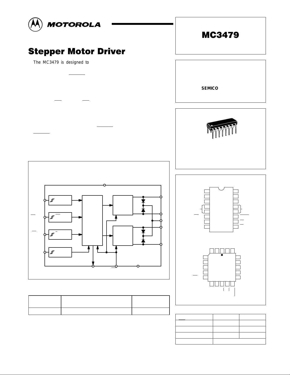
The MC3479 is designed to drive a two–phase stepper motor in the
bipolar mode. The circuit consists of four input sections, a logic
decoding/sequencing section, two driver–stages for the motor coils, and an
output to indicate the Phase A
• Single Supply Operation: 7.2 to 16.5 V
• 350 mA/Coil Drive Capability
• Clamp Diodes Provided for Back–EMF Suppression
• Selectable CW/CCW and Full/Half Step Operation
• Selectable High/Low Output Impedance (Half Step Mode)
• TTL/CMOS Compatible Inputs
• Input Hysteresis: 400 mV Minimum
• Phase Logic Can Be Initialized to Phase A
• Phase A Output Drive State Indication (Open–Collector)
• Available in Standard DIP and Surface Mount
drive state.
Order this document by MC3479/D
STEPPER MOTOR
DRIVER
SEMICONDUCTOR
TECHNICAL DATA
P SUFFIX
PLASTIC PACKAGE
CASE 648C
Figure 1. Representative Block Diagram
V
M
Clock
CW/CCW
/H Step
F
OIC
Logic
/SetPhase A
Driver
Driver
GndBias
CW
Full
Step
Clk
/CCW
/Half
OIC
ORDERING INFORMATION
Operating
Device
MC3479P TA = 0° to +70°C Plastic
Temperature Range
Package
PIN CONNECTIONS
V
V
L3
M
D
20
11 12 13
Full/Half Step
Phase A
CW/CCW
16
15
14
13
12
11
10
9
V
L3
L4
Phase A
CW/CCW
Ful
Step
17
16
15
148
M
Gnd
l/Half
L4
Gnd
Gnd
Gnd
Gnd
1
V
D
2
L1
L2
V
D
L3
L4
L2
3
L1
4
Gnd
5
6
Bias
/Set
Clk
7
8
OIC
(Top View)
L2
L1
21519
3
418
Gnd
Gnd
6
Gnd
7
Gnd
Bias/Set
10
9
Clk
OIC
INPUT TRUTH TABLE
Input Low Input High
CW
/CCW
/Half Step
Full
OIC
CW CCW
Full Step Half Step
Hi Z Low Z
Positive Edge TriggeredClk
MOTOROLA ANALOG IC DEVICE DATA
Motorola, Inc. 1996 Rev 1
1

MC3479
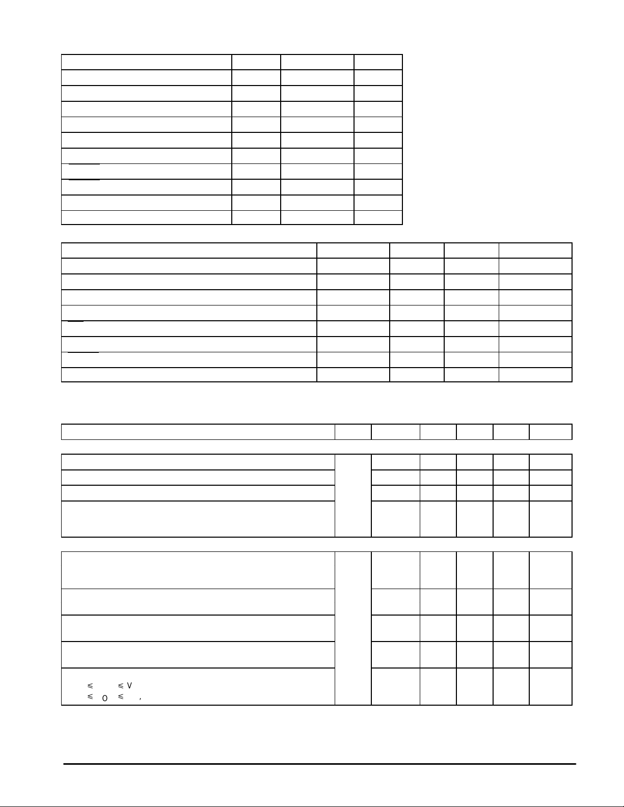
MAXIMUM RATINGS
Rating Symbol Value Unit
Supply Voltage V
Clamp Diode Cathode Voltage (Pin 1) V
Driver Output Voltage V
Drive Output Current/Coil I
Input Voltage (Logic Controls) V
Bias/Set Current I
Phase A Output Voltage V
Phase A Sink Current I
Junction Temperature T
Storage Temperature Range T
M
D
OD
OD
in
BS
OA
OA
J
stg
RECOMMENDED OPERATING CONDITIONS
Characteristic Symbol Min Max Unit
Supply Voltage V
Clamp Diode Cathode Voltage V
Driver Output Current (Per Coil) (Note 1) I
Input Voltage (Logic Controls) V
Bias/Set Current (Outputs Active) I
Phase A Output Voltage V
Phase A Sink Current I
Operating Ambient Temperature T
NOTE: 1. See section on Power Dissipation in Application Information.
+ 18 Vdc
VM + 5.0 Vdc
VM + 6.0 Vdc
± 500 mA
– 0.5 to + 7.0 Vdc
– 10 mA
+ 18 Vdc
20 mA
+ 150 °C
– 65 to + 150 °C
OD
BS
OA
OA
M
D
+ 7.2 + 16.5 Vdc
V
M
VM + 4.5 Vdc
— 350 mA
in
0 + 5.5 Vdc
– 300 – 75 µA
— V
M
Vdc
0 8.0 mA
A
0 + 70 °C
DC ELECTRICAL CHARACTERISTICS (Specifications apply over the recommended supply voltage and temperature range, [Notes
2, 3] unless otherwise noted.)
Characteristic
INPUT LOGIC LEVELS
Threshold Voltage (Low–to–High)
Threshold Voltage (High–to–Low)
Hysteresis V
Current: (VI = 0.4 V)
Current: (VI = 5.5 V)
Current: (VI = 2.7 V)
DRIVER OUTPUT LEVELS
Output High Voltage 2, 3, V
(IBS = – 300 µA): (IOD = – 350 mA)
(IBS = – 300 µA): (IOD = – 0.1 mA)
Output Low Voltage V
(IBS = – 300 µA, IOD = 350 mA)
Differential Mode Output Voltage Difference (Note 4) DV
(IBS = – 300 µA, IOD = 350 mA)
Common Mode Output Voltage Dif ference (Note 5) CV
(IBS = – 300 µA, IOD = – 0.1 mA)
Output Leakage, Hi Z State µA
(0 p VOD p VM, IBS = – 5.0 µA) I
(0 p VOD p VM, IBS = – 300 µA, F/H = 2.0 V, OIC = 0.8 V) I
NOTES: 2. Algebraic convention rather than absolute values is used to designate limit values.
3.Current into a pin is designated as positive. Current out of a pin is designated as negative.
4.DVOD = V
5.CVOD = V
OD1,2
OHD1
– V
– V
OD3,4
OHD2
where: V
or V
OHD3
OD1,2
V
OD3,4
– V
= (V
OHD4
OHD1
= (V
.
– V
OHD3
OLD2
– V
) or (V
OLD4
Pins Symbol Min Typ Max Unit
7, 8,
9, 10
V
V
TLH
THL
HYS
I
IL
— — 2.0 Vdc
0.8 — — Vdc
0.4 — — Vdc
–100
—
—
—
—
+100
—
+20
OHD
14, 15 VM – 2.0
VM – 1.2——
— — 0.8 Vdc
— — 0.15 Vdc
— — 0.15 Vdc
– 100 — + 100
– 100 — + 100
OHD2
) or (V
– V
OHD4
OLD1
– V
), and
OLD3
OLD
OD
OD
OZ1
OZ2
).
—
µA
Vdc
—
—
2
MOTOROLA ANALOG IC DEVICE DATA

MC3479
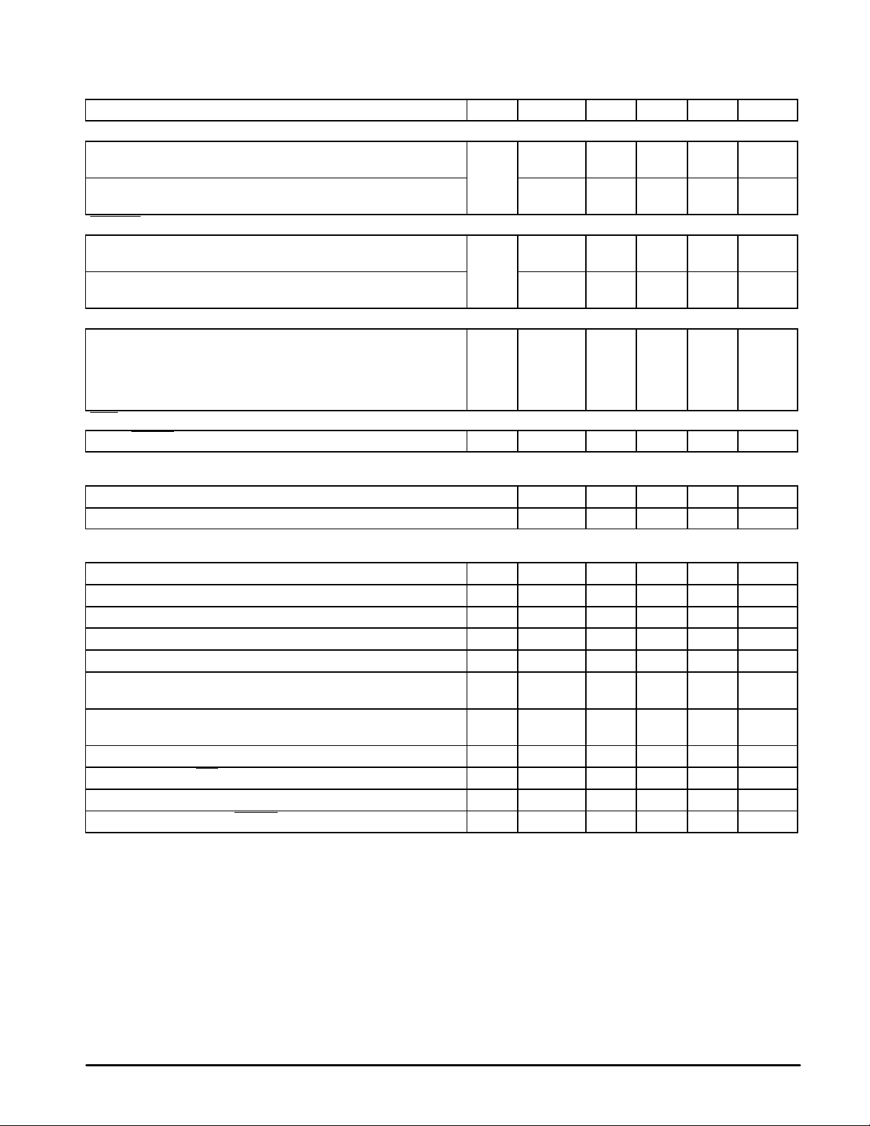
DC ELECTRICAL CHARACTERISTICS (Specifications apply over the recommended supply voltage and temperature range, [Notes
2, 3] unless otherwise noted.)
Characteristic
CLAMP DIODES
Forward Voltage 1, 2, 3, V
(ID = 350 mA) 14, 15
Leakage Current (Per Diode) I
(Pin 1 = 21 V; Outputs = 0 V; IBS = 0 µA)
PHASE A OUTPUT
Output Low Voltage 11 V
(IOA = 8.0 mA)
Off State Leakage Current I
(V
= 16.5 V)
OHA
POWER SUPPLY
Power Supply Current 16 mA
(IOD = 0 µA, IBS = – 300 µA)
(L1 = V
(L1 = V
(L1 = V
BIAS/SET CURRENT
To Set Phase A 6 I
OHD
OHD
OHD
, L2 = V
, L2 = V
, L2 = V
, L3 = V
OLD
, L3 = Hi Z, L4 = Hi Z) I
OLD
, L3 = V
OLD
OHD
OHD
, L4 = V
, L4 = V
) I
OLD
) I
OHD
Pins Symbol Min Typ Max Unit
DF
DR
OLA
OHA
MW
MZ
MN
BS
— 2.5 3.0 Vdc
— — 100 µA
— — 0.4 Vdc
— — 100 µA
— — 70
— — 40
— — 75
– 5.0 — — µA
PACKAGE THERMAL CHARACTERISTICS
Characteristic Symbol Min Typ Max Unit
Thermal Resistance, Junction–to–Ambient (No Heatsink) R
AC SWITCHING CHARACTERISTICS (T
Characteristic
Clock Frequency 7 f
Clock Pulse Width (High) 7 PW
Clock Pulse Width (Low) 7 PW
Bias/Set Pulse Width 6 PW
Setup Time (CW/CCW and F/HS) 10–7
Hold Time (CW/CCW and F/HS) 10–7
Propagation Delay (Clk–to–Driver Output) t
Propagation Delay (Bias/Set–to–Driver Output) t
Propagation Delay (Clk–to–Phase A Low) 7–11 t
Propagation Delay (Clk–to–Phase A High) 7–11 t
NOTES: 2. Algebraic convention rather than absolute values is used to designate limit values.
3.Current into a pin is designated as positive. Current out of a pin is designated as negative.
= + 25°C, VM = 12 V) (See Figures 2, 3, 4)
A
Pins Symbol Min Typ Max Unit
9–7
9–7
θJA
CK
CKH
CKL
BS
t
su
t
h
PCD
PBSD
PHLA
PLHA
— 45 — °C/W
0 — 50 kHz
10 — — µs
10 — — µs
10 — — µs
5.0 — — µs
10 — — µs
— 8.0 — µs
— 1.0 — µs
— 12 — µs
— 5.0 — µs
MOTOROLA ANALOG IC DEVICE DATA
3
 Loading...