Motorola MC3476P1 Datasheet

Device
Operating
Temperature Range
Package
SEMICONDUCTOR
TECHNICAL DATA
LOW COST PROGRAMMABLE
OPERATIONAL AMPLIFIER
ORDERING INFORMATION
MC3476P1 TA = 0° to +70°C Plastic DIP
P1 SUFFIX
PLASTIC PACKAGE
CASE 626
PIN CONNECTIONS
Order this document by MC3476/D
1
8
(Top View)
I
set
V
CC
Output
Offset Null
Offset Null
Invert
Noninvert
V
EE
1
2
3
4
8
7
6
5
+
–
Input
1
MOTOROLA ANALOG IC DEVICE DATA
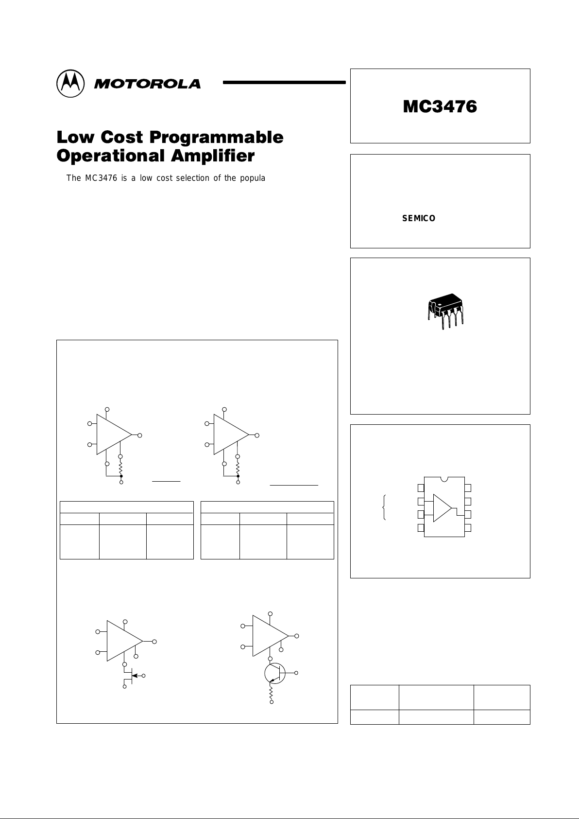
The MC3476 is a low cost selection of the popular industry standard
MC1776 programmable operational amplifier. This extremely versatile
operational amplifier features low power consumption and high input
impedance. In addition, the quiescent currents within the device may be
programmed by the choice of an external resistor value or current source
applied to the I
set
input. This allows the amplifier’s characteristics to be
optimized for input current and power consumption despite wide variations in
operating power supply voltages.
• ±6.0 V to ±18 V Operation
• Wide Programming Range
• Offset Null Capability
• No Frequency Compensation Required
• Low Input Bias Currents
• Short Circuit Protection
Resistive Programming
(See Figure 1)
R
set
to Ground R
set
to Negative Supply
Active Programming
FET Current Source Bipolar Current Source
(Recommended for supply voltage
less than ±6.0 V)
Typical R
set
Values
VCC, VEEI
set
= 1.5 µAI
set
= 15 µA
±6.0 V
±10 V
±12 V
±15 V
3.6 MΩ
6.2 MΩ
7.5 MΩ
10 MΩ
360 kΩ
620 kΩ
750 kΩ
1.0 MΩ
Pins not shown are not connected.
Typical R
set
Values
VCC, VEEI
set
= 1.5 µAI
set
= 15 µA
+
1.5 V
+
3.0 V
+
6.0 V
+
15 V
1.6 MΩ
3.6 MΩ
7.5 MΩ
20 MΩ
160 kΩ
360 kΩ
750 kΩ
2.0 MΩ
VCC – 0.6
R
set
I
set
=
7
2
3
4
8
–
+
R
set
V
EE
I
set
=
VCC – 0.6 – V
EE
R
set
–
+
2
3
7
6
4
8
V
EE
V
G
V
EE
7
2
3
4
8
6
V
EE
R
V
B
V
EE
Q
–
+
6
V
CC
V
CC
7
2
3
4
8
–
+
R
set
V
EE
6
V
CC
Motorola, Inc. 1996 Rev 1

MC3476
2
MOTOROLA ANALOG IC DEVICE DATA
MAXIMUM RATINGS (T
A
= +25°C, unless otherwise noted.)
Rating Symbol Value Unit
Power Supply Voltages VCC, V
EE
±18 Vdc
Input Differential Voltage Range V
IDR
±30 Vdc
Input Common Mode Voltage Range V
ICR
VCC, V
EE
Vdc
Offset Null to VEE Voltage V
off
– V
EE
±0.5 Vdc
Programming Current I
set
200 µA
Programming Voltage V
set
(VCC – 0.6 V) Vdc
(Voltage from I
set
T erminal to Ground) to V
CC
Output Short Circuit Duration (Note 1) t
SC
Indefinite sec
Operating Ambient Temperature Range T
A
0 to +70 °C
Storage Temperature Range T
stg
– 55 ot +125 °C
Junction Temperature T
J
150 °C
NOTES: 1. Short circuit to ground with I
set
v 15 µA. Rating applies up to ambient temperature of +70°C.
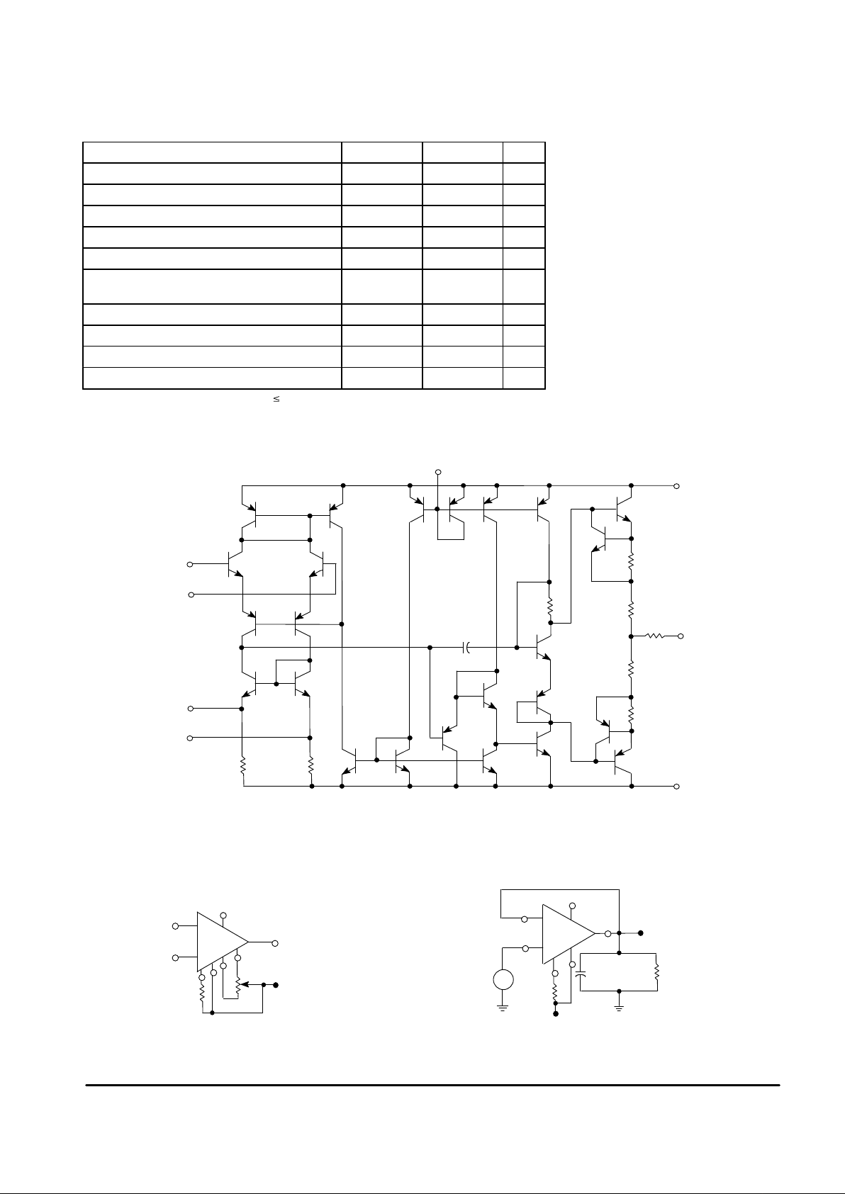
Representative Schematic Diagram
2
3
4
6
7
V
CC
Output
V
EE
50
100
100
50
100
2.0 k
30 pF
10 k
Inputs
8
+
–
1
5
I
set
Offset Null
10 k
Voltage Offset Null Circuit Transient Response Test Circuit
2
3
7
V
CC
6
100 k
V
EE
1
4
8
R
set
–
+
+
–
2
3
7
8
4
6
V
CC
R
set
C
L
R
L
V
O
V
in
Pins not shown are
not connected.
V
EE
5

MC3476
3
MOTOROLA ANALOG IC DEVICE DATA
ELECTRICAL CHARACTERISTICS (V
CC
= +15 V , VEE = – 15 V, I
set
= 15 µA, TA = +25°C, unless otherwise noted).
Characteristic
Symbol Min Typ Max Unit
Input Offset voltage (RS ≤ 10 kΩ) V
IO
mV
TA = +25°C – 2.0 6.0
0°C ≤ TA ≤ +70°C – – 7.5
Offset Voltage Adjustment Range V
IOR
– 18 – mV
Input Offset Current I
IO
nA
TA = +25°C – 20 25
TA = +70°C – – 25
TA = 0°C – – 40
Input Bias Current I
IB
nA
TA = +25°C – 15 50
TA = +70°C – – 50
TA = 0°C – – 100
Input Resistance r
i
– 5.0 – MΩ
Input Capacitance C
i
– 2.0 – pF
Input Common Mode Voltage Gain V
ICR
±10 – – V
0°C ≤ TA ≤ +70°C
Large Signal Voltage Gain A
VOL
V/V
RL ≥ 10 kΩ, VO = ±10 V , TA = +25°C 50 k 400 k –
RL ≥ 10 kΩ, VO = ±10 V , 0° C ≤ TA ≤ +70°C 25 k – –
Output Voltage Range V
OR
V
RL ≥ 10 kΩ, TA = +25°C ±12 ±13 –
RL ≥ 10 kΩ, 0°C ≤ TA ≤ +70°C ±12 – –
Output Resistance r
o
– 1.0 – kΩ
Output Short Circuit Current I
SC
– 12 – mA
Common Mode Rejection CMR 70 90 – dB
RS ≤ 10 kΩ, 0°C ≤ TA ≤ +70°C
Supply Voltage Rejection Ratio PSRR – 25 200 µV/V
RS ≤ 10 kΩ, 0°C ≤ TA ≤ +70°C
Supply Current ICC, I
EE
µA
TA = +25°C – 160 200
0°C ≤ TA ≤ +70°C – – 225
Power Dissipation P
D
mW
TA = +25°C – 4.8 6.0
0°C ≤ TA ≤ +70°C – – 6.75
Transient Response (Unity Gain)
Vin = 20 mV, RL w 10 kΩ, CL = 100 pF
Rise Time t
TLH
– 0.35 – µs
Overshoot os – 10 – %
Slew Rate (RL ≥ 10 kΩ) SR – 0.8 – V/µs
 Loading...