

MOTOROLA MC34280FTB, MC34280FTBR2 Datasheet
MC34280
Power Supply &
Management IC for Handheld
Electronic Products
The MC34280 is a power supply integrated circuit which provides
two boost regulated outputs and some power management supervisory
functions. Both regulators apply Pulse–Frequency–Modulation
(PFM). The main step–up regulator output can be externally adjusted
from 2.7V to 5V. An internal synchronous rectifier is used to ensure
high efficiency (achieve 87%). The auxiliary regulator with a built–in
power transistor can be configured to produce a wide range of positive
voltage (can be used for LCD contrast voltage). This voltage can be
adjusted from +5V to +25V by an external potentiometer; or by a
microprocessor, digitally through a 6–bit internal DAC.
The MC34280 has been designed for battery powered hand–held
products. With the low start–up voltage from 1V and the low quiescent
current (typical 35 µA); the MC34280 is best suited to operate from 1
to 2 AA/ AAA cell. Moreover, supervisory functions such as low
battery detection, CPU power–on reset, and back–up battery control,
are also included in the chip. It makes the MC34280 the best one–chip
power management solution for applications such as electronic
organizers and PDAs.
FEATURES:
• Low Input Voltage, 1V up
• Low Quiescent Current in Standby Mode: 35µA typical
• PFM and Synchronous Rectification to ensure high efficiency
(87% @200mA Load)
• Adjustable Main Output: nominal 3.3V @ 200mA max, with 1.8V
input
• Auxiliary Output Voltage can be digitally controlled by
microprocessor
• Auxiliary Output Voltage:
+5V @ 25mA max, with 1.8V input
+25V @ 15mA max, with 1.8V input
• Current Limit Protection
• Power–ON Reset Signal with Programmable Delay
• Battery Low Detection
• Lithium Battery Back–up
• 32–Pin LQFP Package
32
1
VMAINFB
VBAT
ENABLE
VDD
PDELAY
VREF
AGND
IREF
http://onsemi.com
32–LEAD LQFP
FTB SUFFIX
CASE 873A
MARKING DIAGRAM
MC34280F
TB
AWLYYWW
PIN CONNECTIONS
VMAIN
VMAINSW
VMAINGND
32
1
MC34280
PROB
DGND
LOWBATSEN
A = Assembly Location
WL = Wafer Lot
YY = Year
WW = Work Week
LIBAOUTNCLIBATIN
VAUXEMR
VAUXSW
NC
VAUXBASE
VAUXCHG
VAUXBDV
VAUXFBN
VAUXREF
VAUXFBP
VAUXEN
LIBATCL
LIBATON
LOWBATB
VAUXADJ
VAUXCON
APPLICATIONS:
• Digital Organizer and Dictionary
• Personal Digital Assistance (PDA)
• Dual Output Power Supply (For MPU, Logic, Memory, LCD)
• Handheld Battery Powered Device (1–2 AA/AAA cell)
Semiconductor Components Industries, LLC, 1999
February , 2000 – Rev. 2
1 Publication Order Number:
ORDERING INFORMATION
Device Package Shipping
MC34280FTB LQFP 250 Units/Tray
MC34280FTBR2 LQFP 1800 Tape & Reel
MC34280/D
GND
Riref
r = 480 k
I
REF
MC34280
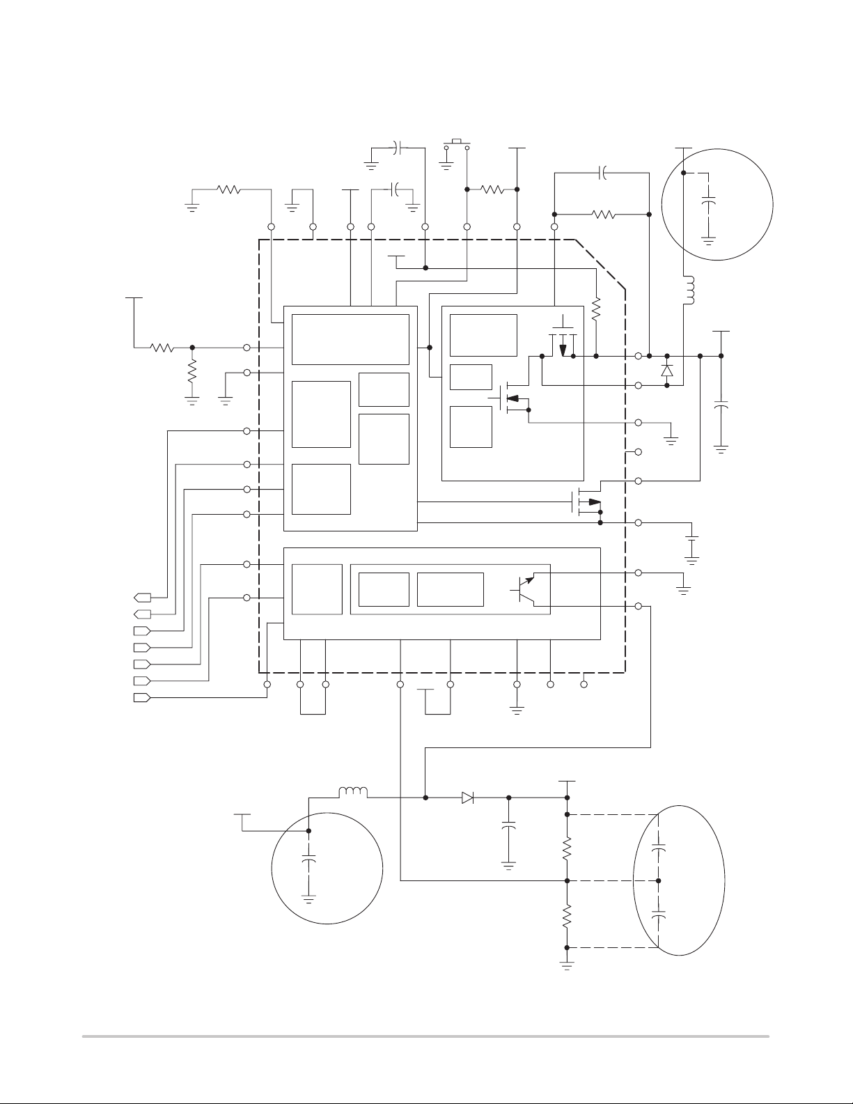
Figure 1. T ypical Application Block Diagram
Battery
4
Lock
Switch
GND
DD
VBAT
Ren
r = 1000 k
ENABLE
321
GND
AGND
V
REF
87
GND
V
REF
65
CVDD
c = 20u
Cpor
c = 80n
GND
PDELAY V
V
DD
VMAINFBVBAT
CMAINb
c = 100p
RMAINb
r = 1000 k
VBAT
Optional
CMAINbp
c = 100u
10 V SMT
tantalum
GND
PORB
LOWBAT
LIBATON
LIBATCL
VAUXADJ
VAUXCON
VAUXEN
VBAT
RLBa
r = 300 k
RLBb
r = 900 k
LOWBATSEN
DGND
GNDGND
PORB
LOWBATB
LIBATON
LIBATCL
VAUXADJ
VAUXCON
VAUXEN
9
10
11
12
13
14
15
16
17
VAUXFBP
R123
Power
ON
Reset
Current
Voltage
Reference
Lithium
Battery
Backup
Level
Control
Auxiliary Regulator
18 20 2119 22 23 24
VAUXREF
(1.1 V to 2.2 V)
Bias
Low
Battery
Detect
Current
Limit
VAUXFBN
VBAT
Control and
Gate Drive
Startup
Current
Limit
Main Regulator with
Synchronous Rectifier
Control and
Base Drive
VAUXBDV
s
M2
d
M1
s
Q1
VAUXBASE
VAUXCHG
r = 5
d
d
s
N/C
32
31
30
29
28
M3
27
26
25
VMAIN
1N5817
VMAINSW
VMAINGND
N/C
LIBATOUT
LIBATIN
VAUXEMR
VAUXSW
LMAIN
L = 33u
(Rs < 60 mOhm)
VMAIN
GND
GND
GND
CMAIN
c = 100u
10 V SMT
tantalum
GND
VBAT
Optional
LAUX
L = 22u
(Rs < 60 mOhm)
CAUXbp
c = 100u
10 V SMT
tantalum
GND
1N5818
30 V SMT
tantalum
http://onsemi.com
2
Caux
c = 30u
GND
VAUX
Rauxb
r = 2.2 M
Rauxa
r = 200 k
GND
Optional
CAUXb
c = 2n
CAUXa
c = 33n
VBAT
ENABLE
VMAIN
PORB
VAUXEN
V
MAINreg
– 0.15 V
MC34280
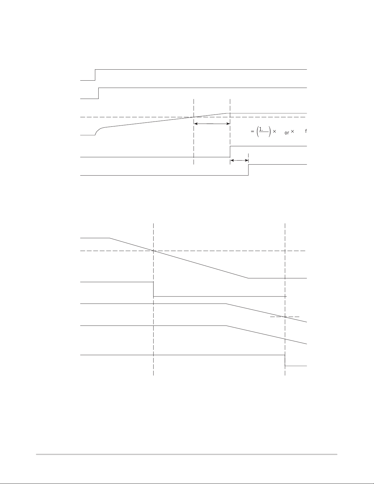
TIMING DIAGRAMS
Figure 2. Startup Timing
T
POR
t
PORC
+
V
MAINreg
1.22
ǒ
0.5
Ǔ
C
RIref
por
VBAT
LOWBATB
VMAIN
ENABLE
PORB
LOWBAT Threshold
Figure 3. Power Down Timing
V
MAINreg
– 0.5 V
http://onsemi.com
3
MC34280
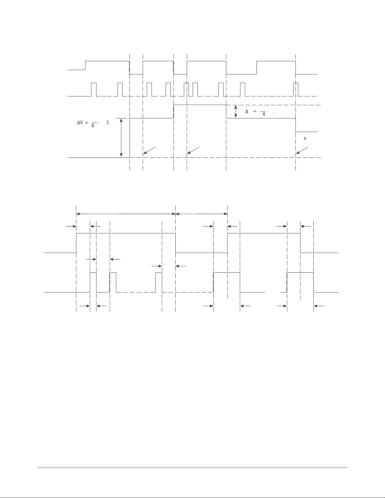
TIMING DIAGRAMS (Con’t)
VAUXCON
VAUXADJ
VAUXREF
1.1 V
T otal N Pulses Total M Pulses
N
DV+
64
@
1.1 V
“Countup”
Flag is HIGH
Figure 4. Auxiliary Regulator Voltage Control
t
CW
t
CL
“Countup”
Flag is LOW
t
CC
M
@
64
1.1 V
t
RJL
Reset
VAUXREF
DV+
t
DL
2.2 V
1.65 V
VAUXCON
VAUXADJ
t
JC
t
JW
t
JL
t
DW
t
RW
Figure 5. Auxiliary Regulator Voltage Control Timing
http://onsemi.com
4
Pin
ББББББ
ББББББ
Á
ББББББ
Á
Á
Á
Á
Á
Á
Á
Á
Á
Á
Á
Á
Á
Á
Á
No.
1
2
3
ÁÁ
4
5
6
7
8
9
10
11
12
13
ÁÁ
14
ÁÁ
15
16
17
18
19
20
21
22
23
24
25
26
27
28
29
ÁÁ
30
31
32
MC34280
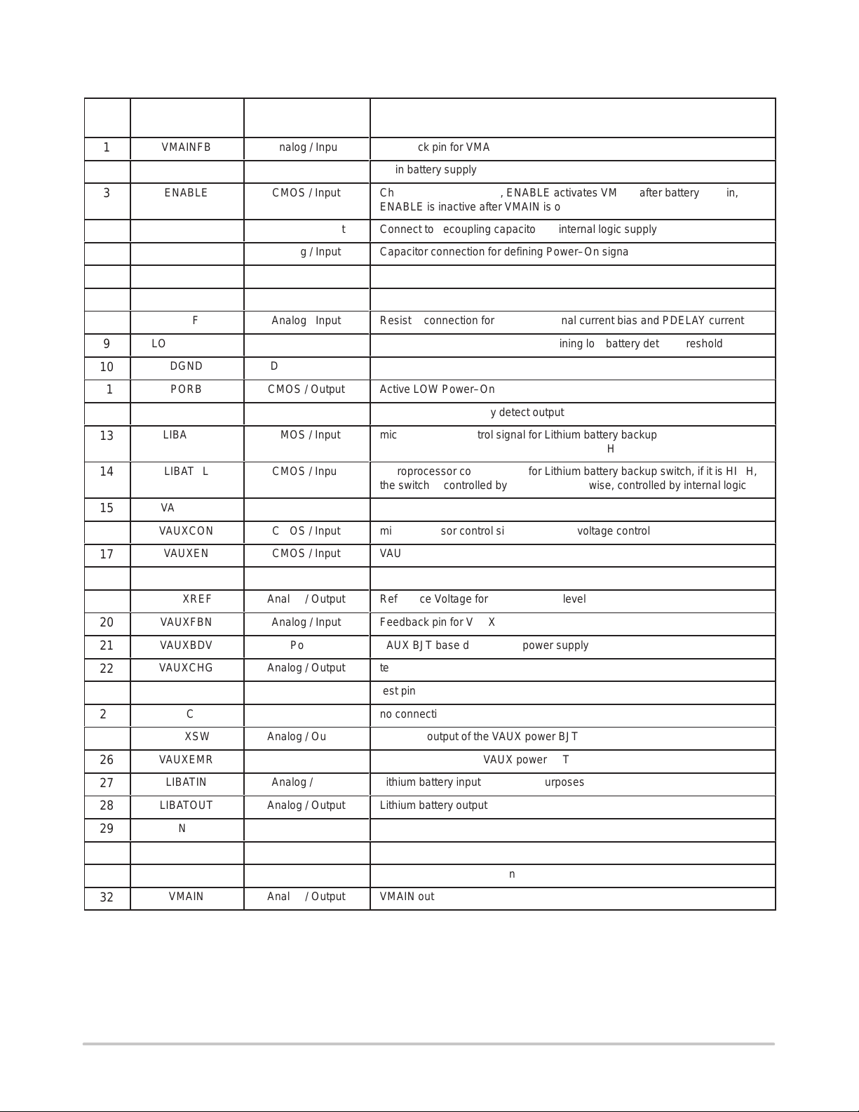
PIN FUNCTION DESCRIPTION
Function Type/Direction Description
VMAINFB
VBAT
ENABLE
ÁÁÁÁ
VDD
PDELAY
VREF
AGND
IREF
LOWBATSEN
DGND
PORB
LOWBATB
LIBATON
ÁÁÁÁ
LIBATCL
ÁÁÁÁ
VAUXADJ
VAUXCON
VAUXEN
VAUXFBP
VAUXREF
VAUXFBN
VAUXBDV
VAUXCHG
VAUXBASE
NC
VAUXSW
VAUXEMR
LIBATIN
LIBATOUT
NC
ÁÁÁÁ
VMAINGND
VMAINSW
VMAIN
Analog / Input
Power
CMOS / Input
БББББ
Analog / Output
Analog / Input
Analog / Output
Feedback pin for VMAIN
Main battery supply
Chip enable, Active high, ENABLE activates VMAIN after battery plug in,
ENABLE is inactive after VMAIN is on
БББББББББББББББББ
Connect to decoupling capacitor for internal logic supply
Capacitor connection for defining Power–On signal delay
Bandgap Reference output voltage. Nominal voltage is 1.25V
Analog Ground
Analog / Input
Analog / Input
Resistor connection for defining internal current bias and PDELAY current
Resistive network connection for defining low battery detect threshold
Digital Ground
CMOS / Output
CMOS / Output
CMOS / Input
БББББ
CMOS / Input
БББББ
CMOS / Input
CMOS / Input
CMOS / Input
Analog / Input
Analog / Output
Analog / Input
Power
Analog / Output
Analog / Output
Active LOW Power–On reset signal
Active LOW low battery detect output
microprocessor control signal for Lithium battery backup switch, the switch is
БББББББББББББББББ
ON when LIBATON=HIGH and LIBATCL=HIGH
microprocessor control signal for Lithium battery backup switch, if it is HIGH,
the switch is controlled by LIBATON, otherwise, controlled by internal logic
БББББББББББББББББ
microprocessor control signal for VAUX voltage control
microprocessor control signal for VAUX voltage control
VAUX enable, Active high
Feedback pin for VAUX
Reference Voltage for VAUX voltage level
Feedback pin for VAUX
VAUX BJT base drive circuit power supply
test pin
test pin
no connection
Analog / Output
Analog / Output
Analog / Input
Analog / Output
БББББÁБББББББББББББББББ
Power Ground
Analog / Input
Analog / Output
Collector output of the VAUX power BJT
Emitter output of the VAUX power BJT
Lithium battery input for backup purposes
Lithium battery output
no connection
Ground for VMAIN low side switch
VMAIN inductor connection
VMAIN output
http://onsemi.com
5
MC34280
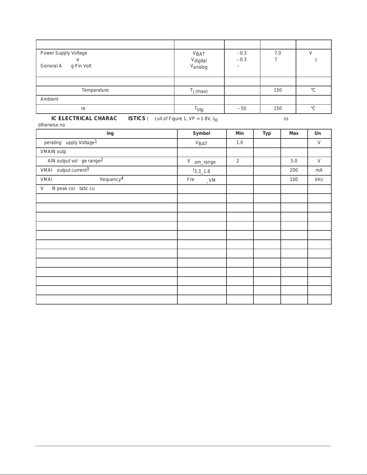
ABSOLUTE MAXIMUM RATINGS (T
Parameter
Power Supply Voltage
Digital Pin Voltage V
General Analog Pin Voltage V
Pin VAUXSW to Pin VAUXEMR Voltage (Continuous) V
Pin VMAINSW to Pin VMAIN Voltage (Continuous)
Operating Junction Temperature
Ambient Operating Temperature
Storage Temperature
STATIC ELECTRICAL CHARACTERISTICS (Circuit of Figure 1, VP = 1.8V, I
= 25°C, unless otherwise noted.)
A
Symbol Min Max Unit
V
BAT
digital
analog
AUXCE
V
syn
Tj
(max)
T
a
T
stg
load
–0.3
7.0
–0.3 7.0 Vdc
–0.3 7.0 Vdc
–0.3 30 Vdc
0.3
150
0
–50
70
150
= 0 mA, TA = 0 to 70°C unless
Vdc
Vdc
°C
°C
°C
otherwise noted.)
Rating
Operating Supply Voltage
1
VMAIN output voltage V
VMAIN output voltage range
VMAIN output current
VMAIN maximum switching frequency
2
3
4
VMAIN peak coil static current limit I
Symbol Min Typ Max Unit
V
BAT
main
V
main_range
I
3.3_1.8
Freq
max_VM
LIM_VM
1.0 V
3.13 3.3 3.47 V
2.7 5.0 V
200 mA
100 kHz
0.85 1.0 1.15 A
VAUX output voltage range VAUX_range 5.0 25 V
VAUXREF lower level voltage VAUX
VAUXREF upper level voltage VAUX
VAUXREF step size VAUX
VAUX maximum switching frequency Freq
VAUX peak coil static current limit I
Quiescent Supply Current at Standby Mode
5
Reference Voltage @ no load Vref
Battery Low Detect lower hysteresis threshold
6
Battery Low Detect upper hysteresis threshold V
PDELAY Pin output charging current Ichg
PDELAY Pin voltage threshold Vth
NOTE: 1. Output current capability is reduced with supply voltage due to decreased energy transfer. The supply voltage must not be higher than
NOTE: 2. Output voltage can be adjusted by external resistor to the VMAINFB pin.
NOTE: 3. At VBAT = 1.8V, output current capability increases with VBAT .
NOTE: 4. Only when current limit is not reached.
NOTE: 5. This is average current consumed by the IC from VDD, which is low–pass filtered from VMAIN, when only VMAIN is enabled and at no loading.
NOTE: 6. This is the minimum of ”LOWBATB” threshold for battery voltage, the threshold can be increased by external resistor divider from ”VBA T” to
VMAIN+0.6V to ensure boost operation. Max Start–up loading is typically 1V at 400 µA, 1.8V at 4.4 mA, and 2.2V at 88 mA.
”LOWBATSEN”.
REF_L
REF_H
REF_S
max_VL
LIM_VL
Iq
standby
no_load
V
LOBAT_L
LOBAT_H
PDELAY
PDELAY
1.0 1.1 1.2 V
2.0 2.2 2.4 V
17 mV
120 kHz
1.0 A
35 60 µA
1.19 1.22 1.25 V
0.8 0.85 0.9 V
1.05 1.1 1.15 V
0.8 1.0 1.2 µA
1.19 1.22 1.25 V
http://onsemi.com
6
 Loading...