

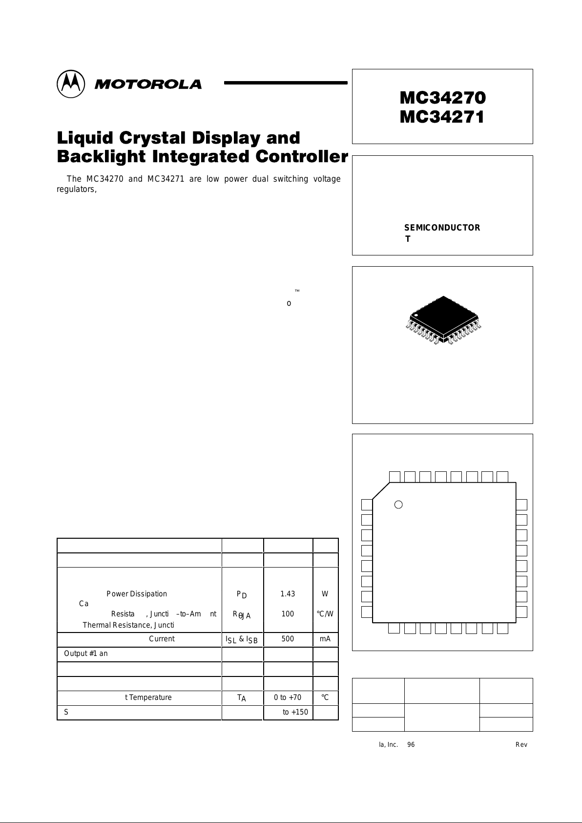
Motorola MC34270FB, MC34271FB Datasheet
EN
2
Device
Operating
Temperature Range
Package
SEMICONDUCTOR
TECHNICAL DATA
LIQUID CRYSTAL DISPLAY
AND BACKLIGHT
INTEGRATED CONTROLLER
ORDERING INFORMATION
MC34270FB
MC34271FB
TA = 0° to +70°C
QFP–32
QFP–32
FB SUFFIX
PLASTIC PACKAGE
CASE 873
1
32
PIN CONNECTIONS
Order this document by MC34270/D
32
DS
1
Ref
1
FB
1
Comp
1
SS
1
S
1
D
1
Drv
1
DS
2
Ref
2
FB
2
Comp
2
SS
2
S
2
D
2
V
B
SW
Sync
R
Gnd
V
T
A
V
ref
ELD
Mode
V
V
DD
3
V
4
V2V1V
0
1
EN
1
31 30 29 2728 26 25
124
23
22
21
20
19
18
17
2
3
4
5
6
7
8
9101112 1413 15 16
1
MOTOROLA ANALOG IC DEVICE DATA
The MC34270 and MC34271 are low power dual switching voltage
regulators, specifically designed for handheld and laptop applications, to
provide several regulated output voltages using a minimum of external parts.
Two uncommitted switching regulators feature a very low standby bias
current of 5.0 µA, and an operating current of 7.0 mA capable of supplying
output currents in excess of 200 mA.
Both devices have three additional features. The first is an ELD Output
that can be used to drive a backlight or a liquid crystal display. The ELD
output frequency is the clock divided by 256. The second feature allows
four additional output bias voltages, in specific proportions to VB, one of the
switching regulated output voltages. It allows use of mixed logic circuitry and
provides a voltage bias for N–Channel load control MOSFETst. The third
feature is an Enable input that allows a logic level signal to turn–“off” or
turn–“on” both switching regulators.
Due to the low bias current specifications, these devices are ideally suited
for battery powered computer, consumer , and industrial equipment where an
extension of useful battery life is desirable.
MC34270 and MC34271 Features:
• Low Standby Bias Current of 5.0 µA
• Uncommitted Switching Regulators Allow Both Positive and Negative
Supply Voltages
• Logic Enable Allows Microprocessor Control of All Outputs
• Synchronizable to External Clock
• Mode Commandable for ELD and LCD Interface
• Frequency Synchronizable
• Auxiliary Output Bias Voltages Enable Load Control via N–Channel FETs
MOSFET is a trademark of Motorola, Inc.
MAXIMUM RATINGS (T
A
= 25°C, unless otherwise noted.)
Rating Symbol Value Unit
Input Voltage
V
DD
ÁÁÁÁ
16
Vdc
БББББББББББ
Á
Power Dissipation and
Thermal Characteristics
ÁÁ
Á
ÁÁÁÁ
ÁÁÁÁÁ
Á
Maximum Power Dissipation P
D
1.43 W
Case 873
Thermal Resistance, Junction–to–Ambient R
θJA
100 °C/W
Thermal Resistance, Junction–to–Case R
θJC
60 °C/W
Output #1 and #2 Switch Current
ISL & I
SB
500
mA
Output #1 and #2 “Off”–State V oltage
V
SL
60
Vdc
Feedback Enable MOSFETs “Off”–State Voltage
V
LF
20
Vdc
Operating Junction Temperature
T
J
125
°C
Operating Ambient Temperature
T
A
0 to +70
°C
БББББББББББ
Storage Temperature Range
ÁÁ
T
stg
ÁÁÁ
–55 to +150Á°C
Motorola, Inc. 1996 Rev 1
MC34270 MC34271
2
MOTOROLA ANALOG IC DEVICE DATA
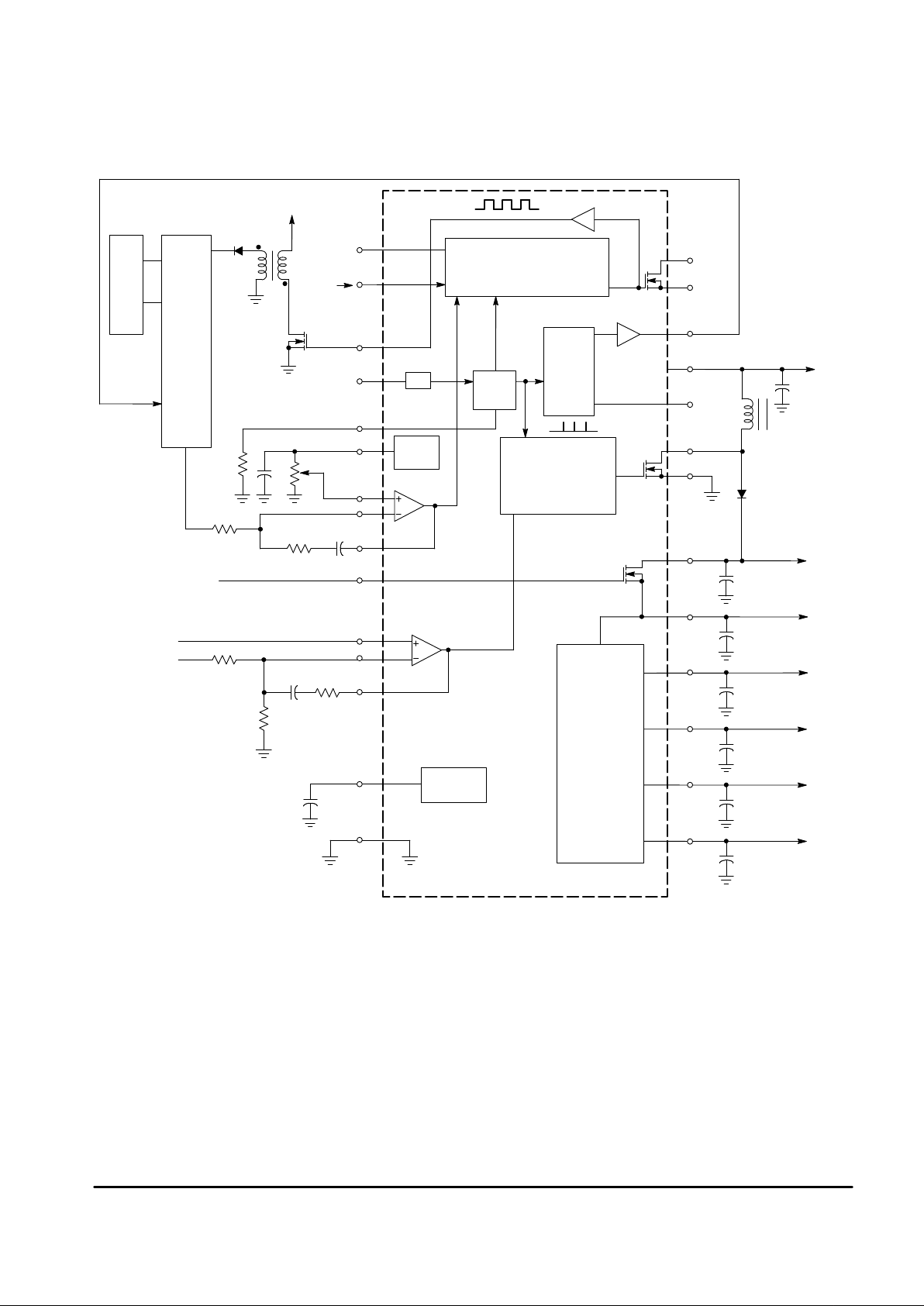
Representative Block Diagram
This device contains 350 active transistors.
V
in
D
1
S
1
SW
1
Sync
Drv
1
EN
1
ELD
Mode
R
T
V
ref
1.25 V
Ref
1
FB
1
V
DD
Comp
1
OSC
D
2
S
2
V
B
V
0
V
1
V
2
V
3
V
4
Ref
2
FB
2
Comp
2
VA = 5.0 V
Gnd
BIAS
V
B
V
2
V
3
V
4
16
15
14
13
12
19
18
17
10
11
9
6
7
32
26
8
31
30
27
2
3
4
23
22
21
28
29
On/Off
From DAC
÷
2
V
1
V
0
BIAS Output
Buffers
V
B
25
µ
P Control
EL
Control
EL
Panel
V
in
EN
2
V
DD
Circuit #1
PWM
Circuit #2
PWM
ELD
EN
V
Ref
V
DD
MC34270 MC34271
3
MOTOROLA ANALOG IC DEVICE DATA
ELECTRICAL CHARACTERISTICS (V
DD
= 6.0 V , for typical values TA = Low to High [Note 1], for min/max values TA is
the operating ambient temperature range that applies, unless otherwise noted.)
Characteristic
Symbol Min Typ Max Unit
REFERENCE SECTION
Reference Voltage (TJ = 25°C) V
ref
1.225 1.250 1.275 V
Line Regulation (VDD = 5.0 V to 12.5 V) Reg
line
– 2.0 10 mV
Load Regulation (IO = 0 to 120 µA) Reg
load
– 2.0 10 mV
Total Variation (Line, Load and Temperature) V
ref
1.215 – 1.285 V
ERROR AMPLIFIERS
Input Offset Voltage (VCM = 1.25 V) V
IO
– 1.0 10 mV
Input Bias Current (VCM = 1.25 V) I
IB
– 120 600 nA
Open Loop Voltage Gain (VCM = 1.25 V , V
COMP
= 2.0 V) A
VOL
80 100 – dB
Output Voltage Swing V
High State (IOH = –100 µA) Ve
OH
VA–1.5 4.0 5.5
Low State (IOL = 100 µA) Ve
OL
0 – 1.0
BIAS VOLTAGE
Voltage (VDD = 5.0 V to 12.5 V, IO = 0) V
A
4.6 5.0 5.4 V
OSCILLATOR AND PWM SECTIONS
Total Frequency Variation Over Line and Temperature f
OSC
kHz
VDD = 5.0 V to 10 V, TA = 0° to 70°C, RT = 169 k 90 115 140
Duty Cycle at Each Output %
Maximum DC
max
92 95 –
Minimum DC
min
– – 0
Sync Input
Input Resistance (V
sync
= 3.5 V) R
sync
25 50 100 kΩ
Minimum Sync Pulse Width T
p
– 1.0 – µs
OUTPUT MOSFETs
Output Voltage – “On”–State (I
sink
= 200 mA) V
OL
– 150 250 mV
Output Current – “Off”–State (VOH = 40 V) I
OH
– 0.1 1.0 µA
Rise and Fall Times tr, t
f
– 50 – ns
EL DISCHARGE OUTPUT (ELD) AND DRV
1
Output Voltage – “On”–State (I
sink
= 100 µA) V
OL
– 30 100 mV
Output Voltage – “On”–State (I
sink
= 50 mA) V
OL
– 2.0 2.5 V
Output Voltage – “Off”–State (I
source
= –100 µA) V
OH
VDD–0.5 5.9 – V
Output Voltage – “Off”–State (I
source
= –50 mA) V
OH
VDD–3.5 3.3 – V
FEEDBACK ENABLE SWITCHES (DS1, DS2)
Output Voltage – “Low”–State (I
sink
= 1.0 mA) Vfe
OL
– 10 100 mV
Output Current – “Off”–State (VOH = 12.5 V) Ife
OH
– 0.6 1.0 µA
SWITCHED VDD OUTPUT (SW1)
Output Voltage V
Switch “On” (EN1 = 1, I
source
= 100 µA) Vsw
OH
5.5 5.9 6.0
Switch “Off” (EN1 = 0, I
sink
= 100 µA) Vsw
OL
0 0.1 0.2
AUXILIARY VOLTAGE OUTPUTS
V0 Enable Switch
“On”–Resistance: VB to V
0
Rds 0 2.0 10 Ω
“Off”–State Leakage Current (VB = 10 V) I
lkg
0 0.1 2.0 µA
V0 Voltage (VB = 30 V, I
source
= 0 mA) V
0
29.5 29.9 30 V
V0 Resistance (I
source
= 4.0 mA) R
0
20 40 60 Ω
NOTE: 1. Low duty pulse techniques are used during test to maintain junction temperature as close to ambient as possible.
MC34270 MC34271
4
MOTOROLA ANALOG IC DEVICE DATA
ELECTRICAL CHARACTERISTICS
(continued) (VDD = 6.0 V , for typical values TA = Low to High [Note 1], for min/max values TA is
the operating ambient temperature range that applies, unless otherwise noted.)
Characteristic UnitMaxTypMinSymbol
AUXILIARY VOLTAGE OUTPUTS
V1, V2, V3, V4 Outputs
1–V1/V0 Ratio: MC34270 0.0565 0.0580 0.0595
MC34271 0.0500 0.0520 0.0535
1–V2/V0 Ratio: MC34270 0.1135 0.1160 0.1185
MC34271 0.1010 0.1035 0.1065
V3/V0 Ratio: MC34270 0.1135 0.1 160 0.1 185
MC34271 0.1010 0.1035 0.1065
V4/V0 Ratio: MC34270 0.0565 0.0580 0.0595
MC34271 0.0500 0.0520 0.0535
Output Resistance (I
source
= 4.0 mA) R
o
20 40 60 Ω
Output Short Circuit Current I
ss
5.0 10 20 mA
LOGIC INPUTS (EN1, EN2, MODE)
Input Low State V
IL
0 – 0.8 V
Input High State V
IH
2.0 – 6.0 V
Input Impedance R
in
25 50 100 kΩ
SOFT START CONTROL (SS1,SS2)
Charge Current (Capacitor Voltage = 1.0 V to 4.0 V)
I
chg
0.5 1.0 2.5 µA
Discharge Current (Capacitor Voltage = 1.0 V) I
dschg
250 650 – µA
TOTAL SUPPLY CURRENT
VDD Current VDD = 6.0 V I
CC
– 2.0 5.0 µA
Standby Mode (EN1 = EN2 = 0) VDD = 16 V – 3.0 15
VDD Current I
CC
– 0.7 3.0 mA
Backlight “On” (EN1 = 1; EN2 = 0)
VDD Current I
CC
– 0.9 2.0 mA
LCD “On” (No Inductor) (EN1 = 0; EN2 = 1)
VB Current (V0 = 35 V) I
O
– 1.2 3.0 mA
NOTE: 1. Low duty pulse techniques are used during test to maintain junction temperature as close to ambient as possible.
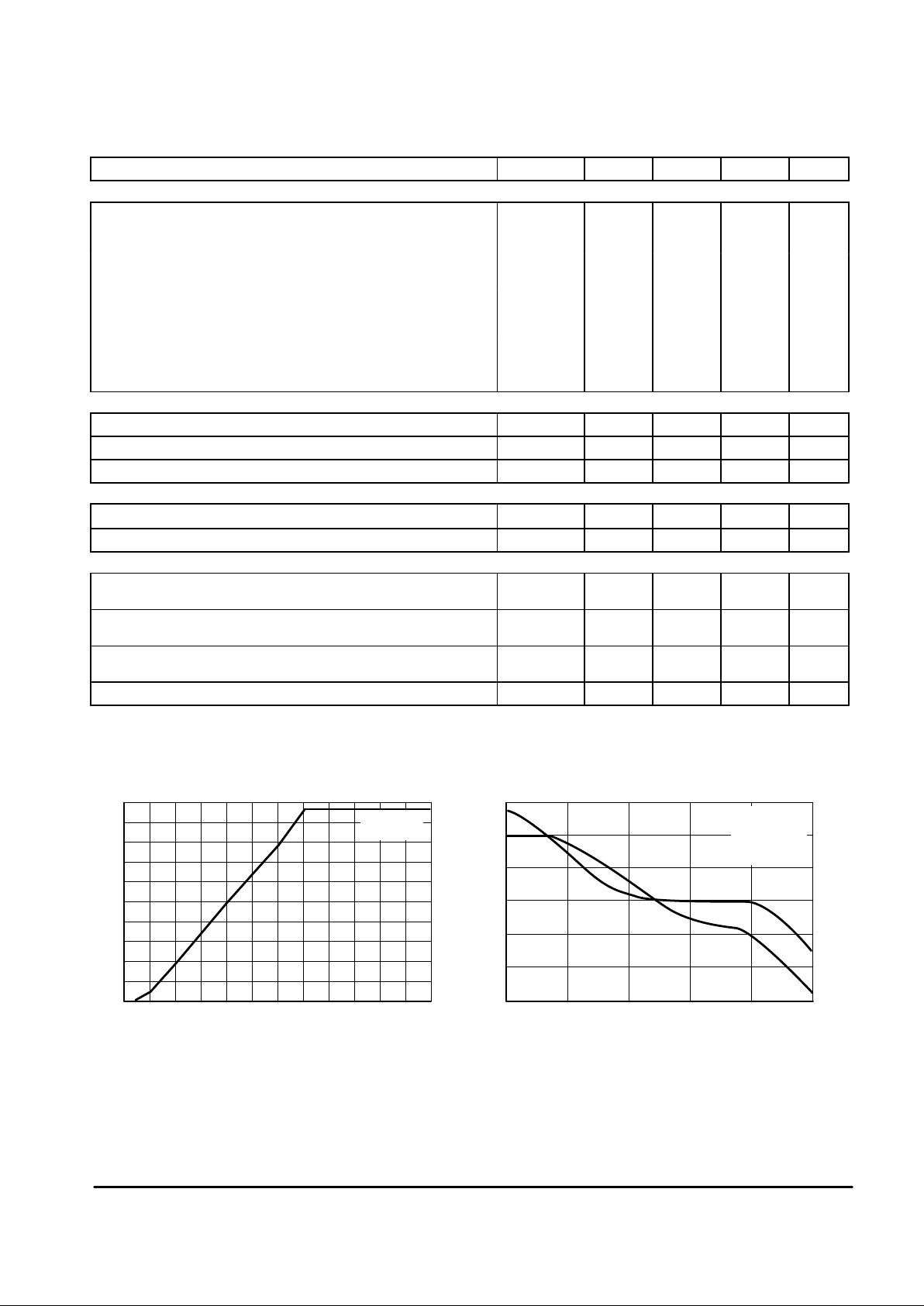
10
100
1.5
1.0
A
VOL
, OPEN LOOP VOL TAGE GAIN (dB)
f, FREQUENCY (Hz)
DC, SWITCH OUTPUT DUTY CYCLE
Figure 1. Switch Output Duty Cycle versus
Compensation Voltage
V
Comp
, COMPENSATION VOLTAGE (V)
Figure 2. Error Amp Open Loop Gain and
Phase versus Frequency
0.6
0.4
0.2
0
0.8
80
60
40
20
0
–20
2.0 2.5 3.0 3.5 4.0 4.5 100 1.0 k 10 k 100 k 1000 k
θ
, EXCESS PHASE ( )
90
120
150
180
°
VDD = 6.0 V
TA = 25
°
C
VDD = 6.0 V
V
Comp
= 2.5 V
RL = Open
TA = 25
°
C
0
30
60
Gain
Phase
 Loading...