

MOTOROLA MC34268D, MC34268DR2, MC34268DT, MC34268DTRK Datasheet
MC34268
SCSI-2 Active Terminator
Regulator
The MC34268 is a medium current, low dropout positive voltage
regulator specifically designed for use in SCSI–2 active termination
circuits. This device offers the circuit designer an economical
solution for precision voltage regulation, while keeping power losses
to a minimum. The regulator consists of a 1.0 V dropout composite
PNP/NPN pass transistor, current limiting, and thermal limiting.
These devices are packaged in the 8–pin SOP–8 and 3–pin DPAK
and SOT–223 surface mount power packages.
Applications include active SCSI–2 terminators and post
regulation of switching power supplies.
• 2.85 V Output Voltage for SCSI–2 Active Termination
• 1.0 V Dropout
• Output Current in Excess of 800 mA
• Thermal Protection
• Short Circuit Protection
• Output Trimmed to 1.4% Tolerance
• No Minimum Load Required
• Space Saving DPAK, SOT–223 and SOP–8 Surface Mount Power
Packages
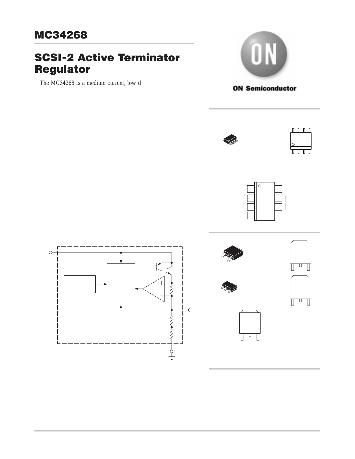
Simplified Block Diagram
http://onsemi.com
Gnd
SOP–8
D SUFFIX
CASE 751
1
2
3
4
(Top View)
8
1
A = Assembly Location
L = Wafer Lot
Y = Year
W = Work Week
Output Output
Input
MARKING
DIAGRAMS
8
1
NC
8
7
6
NC
5
34268
ALYW
Input
Thermal
Limiting
Control
Circuit
Current
Limit
Ground
Output
DPAK
1
3
1
3
Heatsink surface (shown as terminal 4 in
case outline drawing) is connected to Pin 2.
DT SUFFIX
CASE 369A
SOT–223
ST SUFFIX
CASE 318E
4
123
(Top View)
Pin 1. Ground
2. Output
3. Input
4. Output
34268
ALYWW
AYW
268ST
ORDERING INFORMATION
See detailed ordering and shipping information in the package
dimensions section on page 3 of this data sheet.
Semiconductor Components Industries, LLC, 2000
April, 2000 – Rev. 1
1 Publication Order Number:
MC34268/D
MC34268
–
,
O
O
T
OLT
G
(
)
N
MAXIMUM RATINGS
Rating Symbol Value Unit
Power Supply Input Voltage V
Power Dissipation and Thermal Characteristics
DT Suffix, Plastic Package, Case 369A
TA = 25°C, Derate Above TA = 25°C
Thermal Resistance, Junction–to–Case
Thermal Resistance, Junction–to–Air
D Suffix, Plastic Package, Case 751
TA = 25°C, Derate Above TA = 25°C
Thermal Resistance, Junction–to–Case
Thermal Resistance, Junction–to–Air
ST Suffix, Plastic Package, Case 318E
TA = 25°C, Derate Above TA = 25°C
Thermal Resistance, Junction–to–Case
Thermal Resistance, Junction–to–Air
Operating Junction Temperature Range T
Storage Temperature T
R
R
R
R
R
R
P
θJC
θJA
P
θJC
θJA
P
θJC
θJA
stg
in
D
D
D
J
ELECTRICAL CHARACTERISTICS
(Vin = 4.25 V, CO = 10 µF, for typical values TJ = 25°C, for min/max values TJ = 0°C to +125°C, unless otherwise noted.)
Characteristic
Output Voltage (TJ = 25°C, IO = 0 mA)
Output Voltage, over Line, Load, and Temperature (Vin = 3.9 V to 15 V,
IO = 0 mA to 490 mA)
Line Regulation (Vin = 4.25 V to 15 V, IO = 0 mA, TJ = 25°C) Reg
Load Regulation (IO = 0 mA to 800 mA, TJ = 25°C) Reg
Dropout Voltage (IO = 490 mA) Vin–V
Ripple Rejection (f = 120 Hz) RR 55 — — dB
Maximum Output Current (Vin = 5.0 V) I
Bias Current (Vin = 4.25 V, IO = 0 mA) I
Minimum Load Current to maintain Regulation (Vin = 15 V) I
15 V
Internally Limted
5.0
87
Internally Limited
22
140
Internally Limited
15
245
0 to +150 °C
– 55 to +150 °C
Symbol Min Typ Max Unit
V
O
load
(max)
B
L(min)
line
W
°C/W
°C/W
W
°C/W
°C/W
W
°C/W
°C/W
2.81
2.76
— — 0.3 %
— — 0.5 %
— 0.95 1.1 V
O
800 — — mA
— 5.0 to 3.0 8.0 mA
— — 0 mA
2.85
2.85
2.89
2.93
V
Figure 1. Dropout Voltage versus
Figure 2. Transient Load Regulation
Output Load Current
1.5
V
1.3
E
A
1.1
V
U
P
0.9
DR
O
V
0.7
in
V
0.5
0 200 400 600 800 1000
IO, OUTPUT LOAD CURRENT (mA)
TJ = 25°C
Vin = 5.0 V
CO = 10 µF
, OUTPUT VOLTAGE DEVIATIO
O
V
∆
, OUTPUT CURRENTI
O
20 ms/DIV
TA = 25°C
http://onsemi.com
2
MC34268
,
T
M
L
I
T
NC
J
NCTION
TO
I
(
C
)
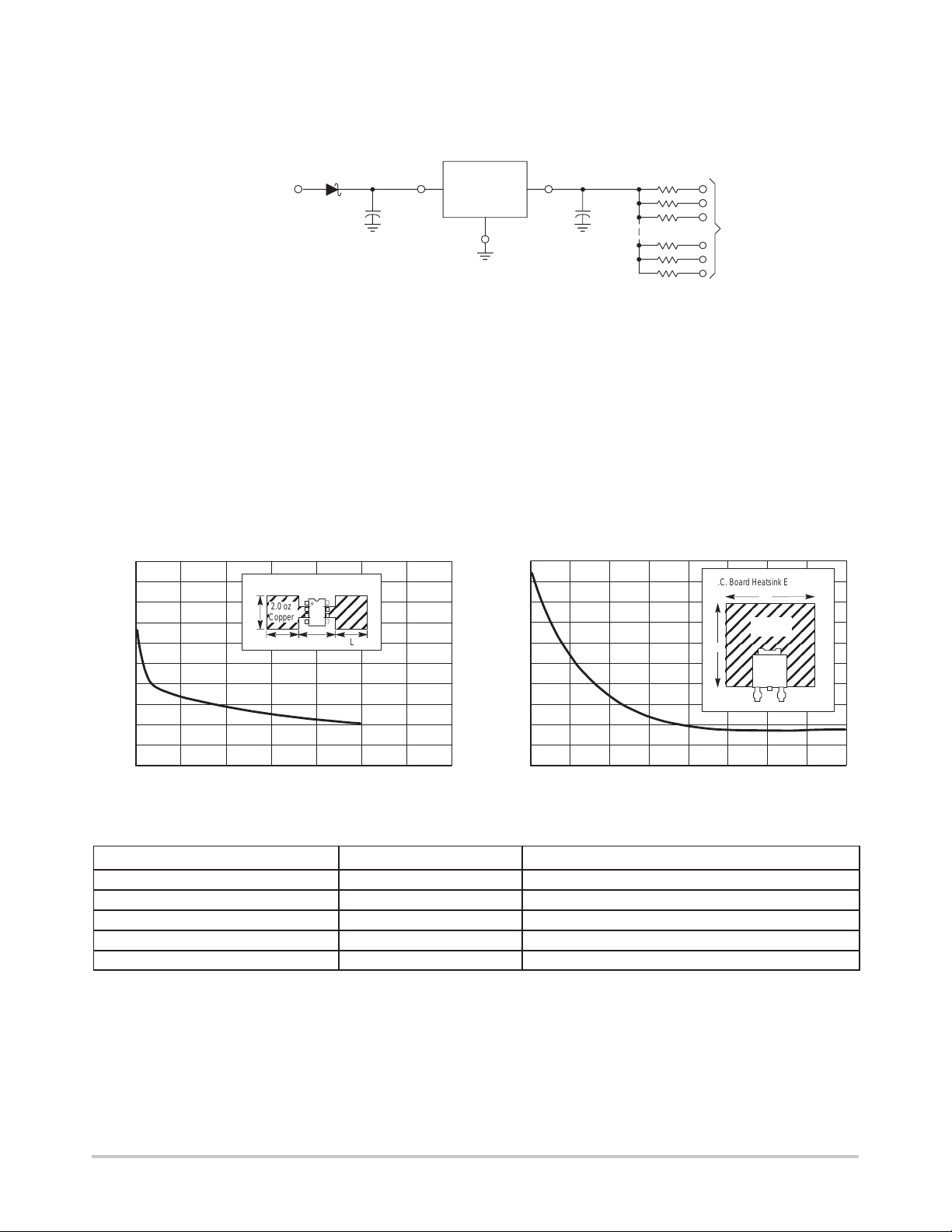
Figure 3. T ypical SCSI Application
V
5.0V
1N5819
in
Figure 3 is a circuit of a typical SCSI terminator
application. The MC34268 is designed specifically to
provide 2.85 V required to drive a SCSI–2 bus. The output
current capability of the regulator is in excess of 800 mA;
enough to drive standard SCSI–2, fast SCSI–2, and some
wide SCSI–2 applications. The typical dropout voltage is
less than 1.0 V, allowing the IC to regulate to input voltages
less than 4.0 V. Internal protective features include current
and thermal limiting.
Figure 4. SOP–8 Thermal Resistance versus
/W
°
R
-A
-
U
E
A
S
180
160
120
80
P.C.B. Copper Length
P.C. Board Heatsink Example
2.0 oz
L
Copper
9.0 mm
L
L
MC34268
SCSI
Regulator
Gnd
V
O
C
1010
O
110Ω
To SCSI Bus
The MC34268 requires an external 10 µF capacitor with
an ESR of less than 10 Ω for stability over temperature.
With economical electrolytic capacitors, cold temperature
operation can pose a stability problem. As temperature
decreases, the capacitance also decreases and the ESR
increases, which could cause the circuit to oscillate.
Tantalum capacitors may be a better choice if small size is
a requirement. Also, the capacitance and ESR of a tantalum
capacitor is more stable over temperature.
Figure 5. DP AK Thermal Resistance
°
90
80
70
60
versus P.C.B. Copper Length
P.C. Board Heatsink Example
L
L
2.0 oz
Copper
RES
40
A
HER
0
0 102030405060
JA
θ
L, LENGTH OF COPPER FLAGS (mm)
70
50
40
, THERMAL RESISTANCE JUNCTION-TO-AIR ( C/W)
0 10203040
JA
θ
L, LENGTH OF COPPER (mm)
ORDERING INFORMATION
Device Package Shipping Information
MC34268D SO–8 98 Units / Rail
MC34268DR2 SO–8 2500 Units / Tape & Reel
MC34268DT DPAK 75 Units / Rail
MC34268DTRK DPAK 2500 Units / Tape & Reel
MC34268STT3 SOT–223 4000 Units / Tape & Reel
http://onsemi.com
3
 Loading...