

Order this document by MC3423/D
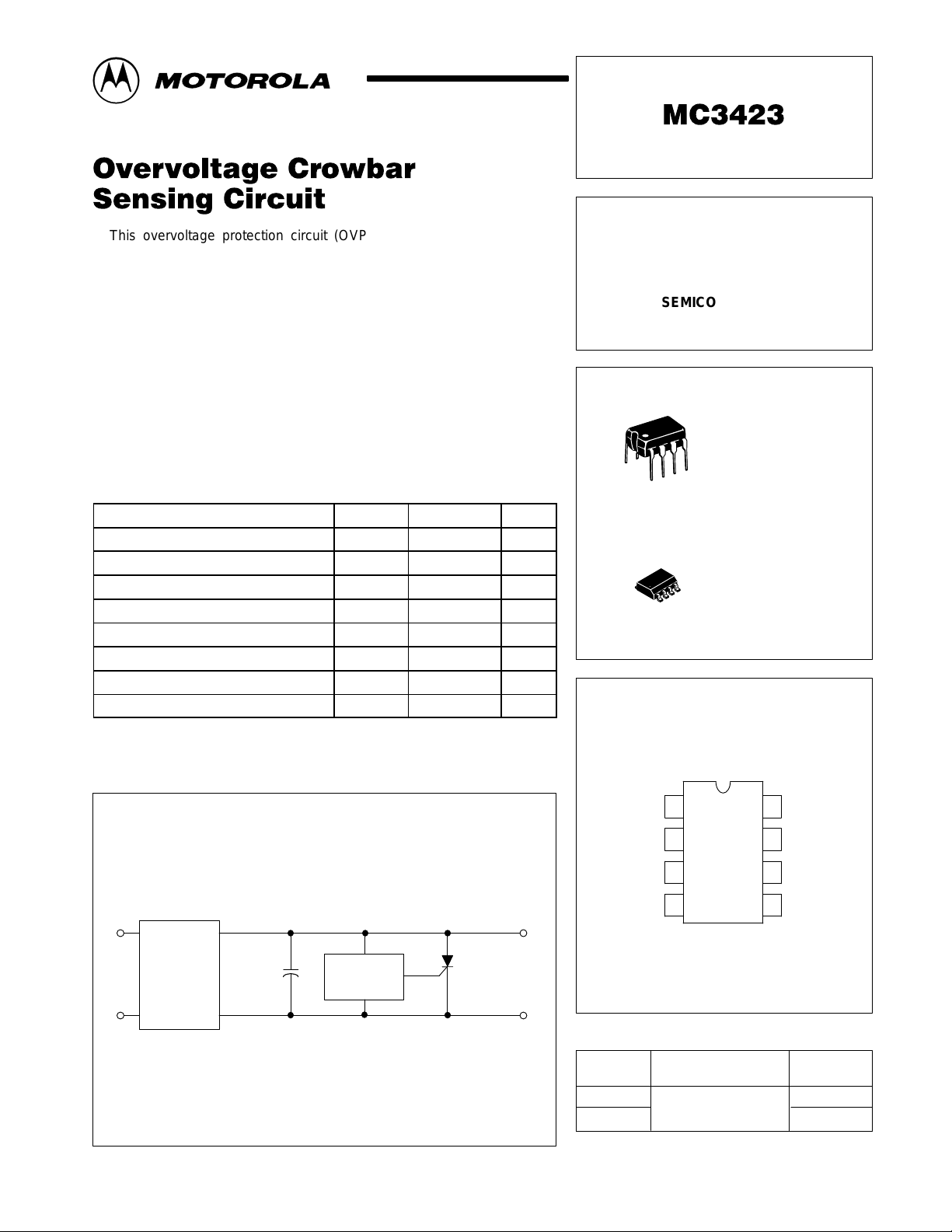
This overvoltage protection circuit (OVP) protects sensitive electronic
circuitry from overvoltage transients or regulator failures when used in
conjunction with an external “crowbar” SCR. The device senses the
overvoltage condition and quickly “crowbars” or short circuits the supply,
forcing the supply into current limiting or opening the fuse or circuit breaker.
The protection voltage threshold is adjustable and the MC3423 can be
programmed for minimum duration of overvoltage condition before tripping,
thus supplying noise immunity .
The MC3423 is essentially a “two terminal” system, therefore it can be
used with either positive or negative supplies.
MAXIMUM RATINGS
Rating Symbol Value Unit
Differential Power Supply Voltage VCC–V
Sense Voltage (1) V
Sense Voltage (2) V
Remote Activation Input Voltage V
Output Current I
Operating Ambient Temperature Range T
Operating Junction Temperature T
Storage Temperature Range T
Sense1
Sense2
act
O
A
stg
EE
J
40 Vdc
6.5 Vdc
6.5 Vdc
7.0 Vdc
300 mA
0 to +70 °C
125 °C
–65 to +150 °C
OVERVOLTAGE
SENSING CIRCUIT
SEMICONDUCTOR
TECHNICAL DATA
P1 SUFFIX
PLASTIC PACKAGE
CASE 626
8
1
D SUFFIX
PLASTIC PACKAGE
8
1
PIN CONNECTIONS
CASE 751
(SOP–8)
Simplified Application
V
in
Current
Limited
DC
Power
Supply
+
C
out
O. V. P.
MC3423
MOTOROLA ANALOG IC DEVICE DATA
1
CC
Sense 1
Sense 2
V
out
2
3
Current
45
Source
(Top View)
Drive
8V
Output
7
V
EE
Indicator
6
Output
Remote
Activation
ORDERING INFORMATION
Operating
Device
MC3423D
MC3423P1
Motorola, Inc. 1996 Rev 1
Temperature Range
TA = 0° to +70°C
Package
SO–8
Plastic DIP
1
MC3423
ELECTRICAL CHARACTERISTICS
Characteristics Symbol Min Typ Max Unit
Supply Voltage Range VCC–V
Output Voltage
(IO = 100 mA)
Indicator Output Voltage
(I
= 1.6 mA)
O(Ind)
Sense Trip V oltage
(TA = 25°C)
Temperature Coefficient of V
(Figure 2)
Remote Activation Input Current
(VIH = 2.0 V, VCC – VEE = 5.0 V)
(VIL = 0.8 V, VCC – VEE = 5.0 V)
Source Current I
Output Current Risetime
(TA = 25°C)
Propagation Delay Time
(TA = 25°C)
Supply Current I
NOTES: T
low
to T
= 0° to +70°C
high
Sense1
(5.0 V ≤ VCC – VEE ≤ 36 V, T
< TA , T
low
VOL(Ind) – 0.1 0.4 Vdc
V
Sense1,
V
Sense2
TCV
Source
, unless otherwise noted.)
high
EE
V
O
S1
I
IH
I
IL
t
r
t
pd
D
4.5 – 40 Vdc
VCC–2.2 VCC–1.8 – Vdc
2.45 2.6 2.75 Vdc
– 0.06 – %/°C
–
–
0.1 0.2 0.3 mA
– 400 – mA/µs
– 0.5 – µs
– 6.0 10 mA
5.0
–120
40
–180
µA
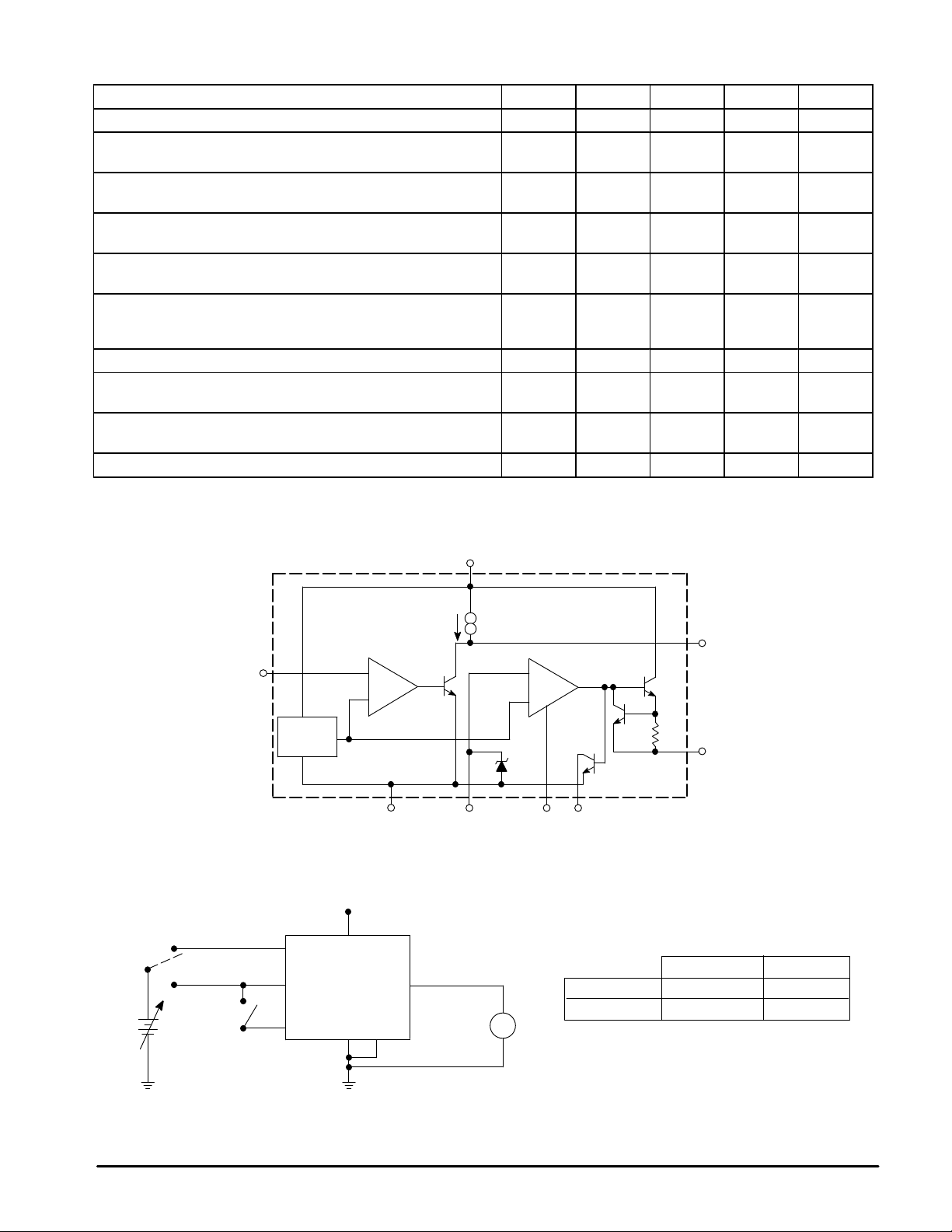
Figure 1. Representative Block Diagram
V
1
CC
I
Sense 1
Source
2
V
ref
2.6V
–
–+
+
+
V
EE
Sense 2
–
6537
Remote
Activation
Indicator
Output
4
Current
Source
8
Output
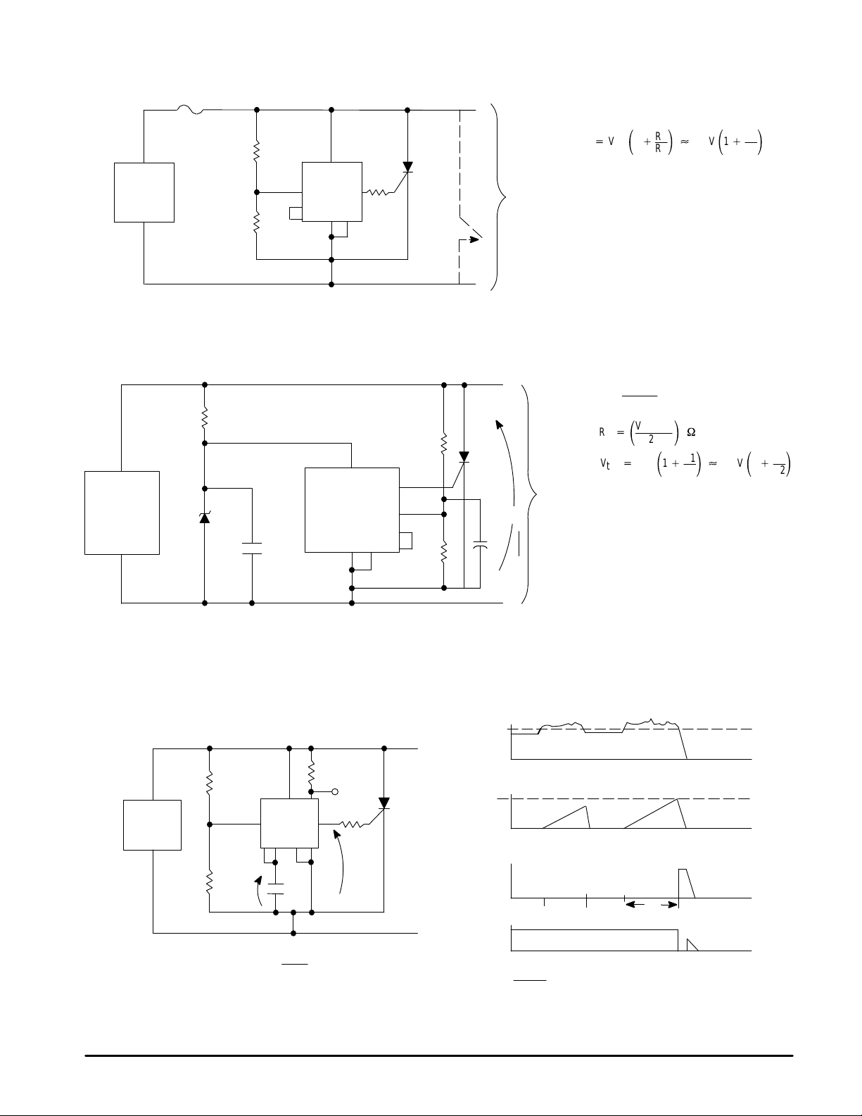
Figure 2. Sense V oltage Test Circuit
V
CC
Switch 1
(A)
(B)
Switch 2
V
I
2
3
4
1
MC3423
75
8
V
V
Sense 1
V
Sense 2
Ramp VI until output goes high; this is
the V
Sense
Switch 1 Switch 2
Position A
Position B
threshold.
Closed
Open
2
MOTOROLA ANALOG IC DEVICE DATA
MC3423
Figure 3. Basic Circuit Configuration
Power
Supply
Power
Supply
F1
1N4740
10V
*
(+ Sense
R1
R2
Lead)
2
3
4
1
MC3423
75
(– Sense Lead)
8
R
G
S1*
+
R1
ǒ
V
+
V
trip
ref
R2 ≤ 10 kΩ for minimum drift
To
Load
–
For minimum value of RG, see Figure 9.
*See text for explanation.
Ǔ
1
)
[
2.6 Vǒ1
R2
R1
Ǔ
)
R2
Figure 4. Circuit Configuration for Supply Voltage Above 36 V
Q1
+
To
Load
V
S
C
1
–
(+ Sense
R
S
1
MC3423
+
µ
F
10
15V
75
Lead)
R1
8
2
3
4
*R2
(– Sense
Lead)
R
S
C1 >
RS+
V
trip
*R2 ≤ 10 k
Q1: VS ≤ 50 V; 2N6504 or equivalent
Q1: VS
Q1: VS
Q1: VS
Q1: V
S
Q1: VS
(R1 + R2) 10
R1R
2
V
S–10
ǒ
25
ǒ
+
V
1
)
ref
Ω
≤
100 V; 2N6505 or equivalent
≤
200 V; 2N6506 or equivalent
≤
400 V; 2N6507 or equivalent
≤
600 V; 2N6508 or equivalent
≤
800 V; 2N6509 or equivalent
µ
F
Ǔ
k
W
R1
Ǔ
[
2.6 Vǒ1
R2
R1
Ǔ
)
R2
Figure 5. Basic Configuration for Programmable Duration
Power
Supply
R1
2
R2
1
6
MC3423
4753
C
R3
≥
C
V
trip
10 mA
V
MOTOROLA ANALOG IC DEVICE DATA
of Overvoltage Condition Before Trip
V
CC
V
trip
+V
R3
V
10
Indication
Out
8
R
G
V
O
CC
0
V
C
V
ref
0
V
O
0
V
IO
td =
I
source
t
d
V
ref
×
C ≈ [12 × 103] C (See Figure 10)
3
MC3423
APPLICATION INFORMATION
Basic Circuit Configuration
The basic circuit configuration of the MC3423 OVP is
shown in Figure 3 for supply voltages from 4.5 V to 36 V , and
in Figure 4 for trip voltages above 36 V . The threshold or trip
voltage at which the MC3423 will trigger and supply gate
drive to the crowbar SCR, Q1, is determined by the selection
of R1 and R2. Their values can be determined by the
equation given in Figures 3 and 4, or by the graph shown in
Figure 8. The minimum value of the gate current limiting
resistor, RG, is given in Figure 9. Using this value of RG, the
SCR, Q1, will receive the greatest gate current possible
without damaging the MC3423. If lower output currents are
required, RG can be increased in value. The switch, S1,
shown in Figure 3 may be used to reset the crowbar.
Otherwise, the power supply, across which the SCR is
connected, must be shut down to reset the crowbar. If a non
current–limited supply is used, a fuse or circuit breaker, F1,
should be used to protect the SCR and/or the load.
The circuit configurations shown in Figures 3 and 4 will
have a typical propogation delay of 1.0 µs. If faster operation
is desired, Pin 3 may be connected to Pin 2 with Pin 4 left
floating. This will result in decreasing the propogation delay to
approximately 0.5 µs at the expense of a slightly increased
TC for the trip voltage value.
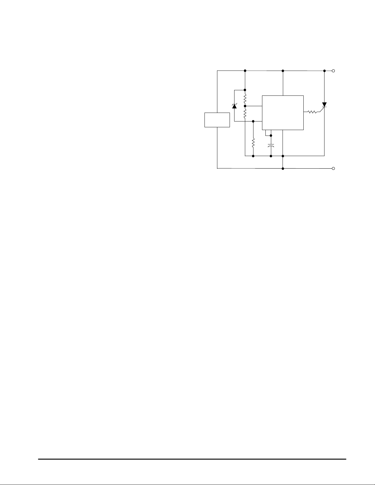
Configuration for Programmable Minimum Duration
of Overvoltage Condition Before Tripping
In many instances, the MC3423 OVP will be used in a
noise environment. To prevent false tripping of the OVP
circuit by noise which would not normally harm the load,
MC3423 has a programmable delay feature. To implement
this feature, the circuit configuration of Figure 5 is used. In
this configuration, a capacitor is connected from Pin 3 to VEE.
The value of this capacitor determines the minimum duration
of the overvoltage condition which is necessary to trip the
OVP . The value of C can be found from Figure 10. The circuit
operates in the following manner: When VCC rises above the
trip point set by R1 and R2, an internal current source (Pin 4)
begins charging the capacitor, C, connected to Pin 3. If the
overvoltage condition disappears before this occurs, the
capacitor is discharged at a rate ≅ 10 times faster than the
charging rate, resetting the timing feature until the next
overvoltage condition occurs.
Occasionally, it is desired that immediate crowbarring of
the supply occur when a high overvoltage condition occurs,
while retaining the false tripping immunity of Figure 5. In this
case, the circuit of Figure 6 can be used. The circuit will
operate as previously described for small overvoltages, but
will immediately trip if the power supply voltage exceeds
VZ1 + 1.4 V.
Figure 6. Configuration for Programmable
Duration of Overvoltage Condition Before
Trip/With Immediate Trip at
High Overvoltages
(+ Sense
Lead)
1
R1
R2
1k
2
MC3423
5
34
7
C
(– Sense Lead)
R
G
3
Z1
Power
Supply
Additional Features
1. Activation Indication Output
An additional output for use as an indicator of OVP
activation is provided by the MC3423. This output is an
open collector transistor which saturates when the OVP is
activated. In addition, it can be used to clock an edge
triggered flip–flop whose output inhibits or shuts down the
power supply when the OVP trips. This reduces or
eliminates the heatsinking requirements for the
crowbar SCR.
2. Remote Activation Input
Another feature of the MC3423 is its remote activation
input, Pin 5. If the voltage on this CMOS/TTL compatible
input is held below 0.8 V, the MC3423 operates normally.
However, if it is raised to a voltage above 2.0 V, the OVP
output is activated independent of whether or not an
overvoltage condition is present. It should be noted that Pin
5 has an internal pull–up current source. This feature can
be used to accomplish an orderly and sequenced
shutdown of system power supplies during a system fault
condition. In addition, the activation indication output of one
MC3423 can be used to activate another MC3423 if a single
transistor inverter is used to interface the former’s indication
output to the latter’s remote activation input, as shown in
Figure 7. In this circuit, the indication output (Pin 6) of the
MC3423 on power supply 1 is used to activate the MC3423
associated with power supply 2. Q1 is any small PNP with
adequate voltage rating.
+
–
4
MOTOROLA ANALOG IC DEVICE DATA

MC3423
Figure 7. Circuit Configuration for
Activating One MC3423 from Another
+
–
+
–
Power
Supply
#1
Power
Supply
#2
1
6
7
R1
10k
1
5
7
Q1
1.0k
Note that both supplies have their negative output leads
tied together (i.e., both are positive supplies). If their
positive leads are common (two negative supplies) the
emitter of Q1 would be moved to the positive lead of supply
1 and R1 would therefore have to be resized to deliver the
appropriate drive to Q1.
Figure 8. R1 versus Trip Voltage
30
Ω
20
10
R1, RESISTANCE (k )
0
0 5.0 10 15 20 25 30
R2 = 2.7 k
VT, TRIP VOLTAGE (V)
Max
Figure 9. Minimum RG versus Supply V oltage
35
R
= 0
30
25
G(min)
if VCC < 11 V
Typ
Min
Crowbar SCR Considerations
Referring to Figure 11, it can be seen that the crowbar
SCR, when activated, is subject to a large current surge from
the output capacitance, C
. This capacitance consists of
out
the power supply output caps, the load’s decoupling caps,
and in the case of Figure 11A, the supply’s input filter caps.
This surge current is illustrated in Figure 12, and can cause
SCR failure or degradation by any one of three mechanisms:
di/dt, absolute peak surge, or I2t. The interrelationship of
these failure methods and the breadth of the applications
make specification of the SCR by the semiconductor
manufacturer difficult and expensive. Therefore, the designer
must empirically determine the SCR and circuit elements
which result in reliable and effective OVP operation.
However, an understanding of the factors which influence the
SCR’s di/dt and surge capabilities simplifies this task.
di/dt
As the gate region of the SCR is driven on, its area of
conduction takes a finite amount of time to grow, starting as a
very small region and gradually spreading. Since the anode
current flows through this turned–on gate region, very high
current densities can occur in the gate region if high anode
currents appear quickly (di/dt). This can result in immediate
destruction of the SCR or gradual degradation of its forward
blocking voltage capabilities – depending on the severity of
the occasion.
20
, SUPPLY VOLTAGE (V)
CC
15
V
10
0 10203040 50 607080
Ω
RG, GATE CURRENT LIMITING RESISTOR (
)
Figure 10. Capacitance versus
Minimum Overvoltage Duration
123571
1.0
0.1
µ
0.01
0.001
C, CAPACITANCE ( F)
0.001 0.01 0.1 1.0 10
td, DELAY TIME (ms)
1
5
2
10.0001
MOTOROLA ANALOG IC DEVICE DATA
5
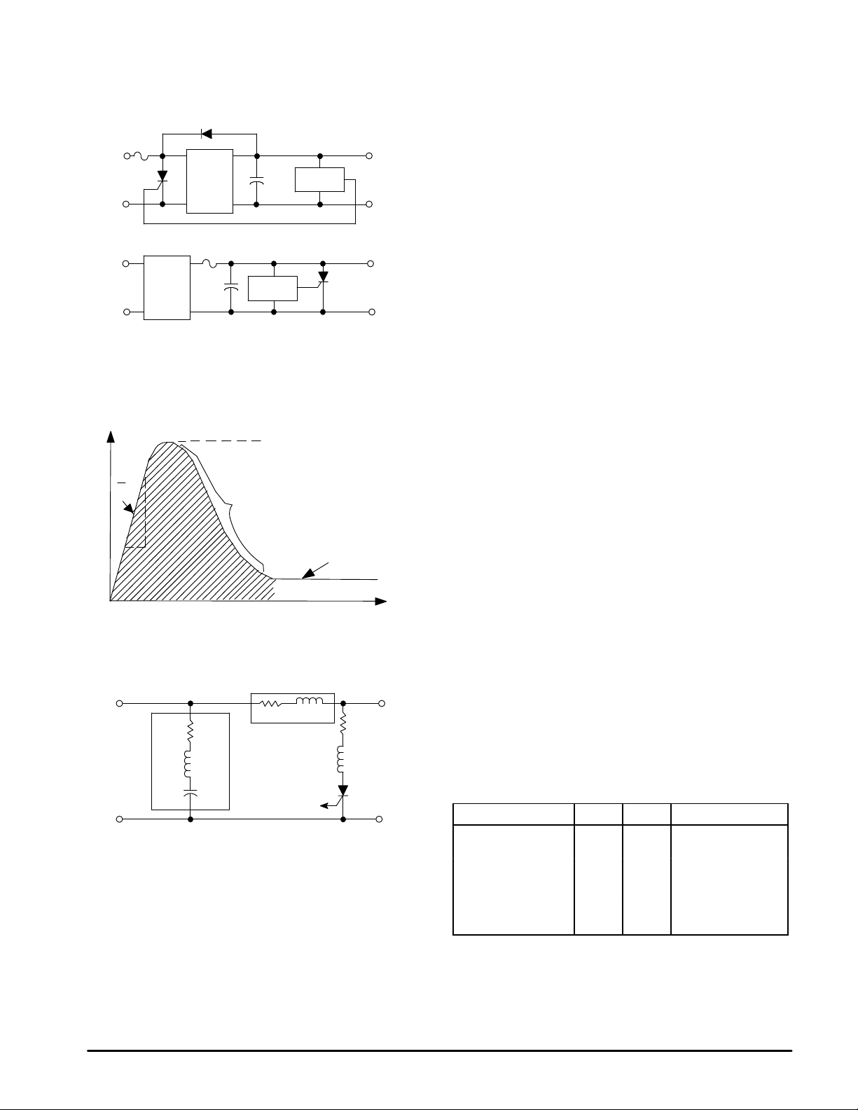
Figure 11. Typical Crowbar OVP Circuit
Configurations
out
(11A)
OV
Sense
(11B)
V
in
DC
Power
Supply
V
in
DC
Power
Supply
*
C
out
*Needed if supply not current limited
+
C
+
OV
Sense
Figure 12. Crowbar SCR Surge Current
Waveform
l
di
dt
l
pk
Surge Due to
Output Capacitor
MC3423
will be the case, though this is difficult to guarantee. Of
course, a sufficiently high surge will cause an open. These
comments also apply to the fuse in Figure 1 1B.
The value of di/dt that an SCR can safely handle is
V
out
V
out
influenced by its construction and the characteristics of the
gate drive signal. A center–gate–fire SCR has more di/dt
capability than a corner–gate–fire type, and heavily
overdriving (3 to 5 times IGT) the SCR gate with a fast < 1.0 µs
rise time signal will maximize its di/dt capability. A typical
maximum number in phase control SCRs of less than 50
A(RMS) rating might be 200 A/µs, assuming a gate current of
five times IGT and < 1.0 µs rise time. If having done this, a
di/dt problem is seen to still exist, the designer can also
decrease the di/dt of the current waveform by adding
inductance in series with the SCR, as shown in Figure 13. Of
course, this reduces the circuit’s ability to rapidly reduce the
DC bus voltage and a tradeoff must be made between
speedy voltage reduction and di/dt.
Surge Current
If the peak current and/or the duration of the surge is
excessive, immediate destruction due to device overheating
will result. The surge capability of the SCR is directly
proportional to its die area. If the surge current cannot be
reduced (by adding series resistance – see Figure 13) to a
safe level which is consistent with the systems requirements
for speedy bus voltage reduction, the designer must use a
higher current SCR. This may result in the average current
capability of the SCR exceeding the steady state current
requirements imposed by the DC power supply.
Current Limited
Supply Output
t
Figure 13. Circuit Elements Affecting
SCR Surge and di/dt
R
LeadLLead
ESR
Output
ESL
R & L EMPIRICALLY DETERMINED!
Cap
To
MC3423
R
L
The usual design compromise then is to use a garden
variety fuse (3AG or 3AB style) which cannot be relied on to
blow before the thyristor does, and trust that if the SCR does
fail, it will fail short circuit. In the majority of the designs, this
A WORD ABOUT FUSING
Before leaving the subject of the crowbar SCR, a few
words about fuse protection are in order. Referring back to
Figure 1 1A, it will be seen that a fuse is necessary if the power
supply to be protected is not output current limited. This fuse
is not meant to prevent SCR failure but rather to prevent a fire!
In order to protect the SCR, the fuse would have to
possess an I2t rating less than that of the SCR and yet have
a high enough continuous current rating to survive normal
supply output currents. In addition, it must be capable of
successfully clearing the high short circuit currents from the
supply. Such a fuse as this is quite expensive, and may not
even be available.
CROWBAR SCR SELECTION GUIDE
As an aid in selecting an SCR for crowbar use, the
following selection guide is presented.
Device I
2N6400 Series 16 A 160 A TO–220 Plastic
2N6504 Series 25 A 160 A TO–220 Plastic
2N1842 Series 16 A 125 A Metal Stud
2N2573 Series 25 A 260 A Metal TO–3 Type
2N681 Series 25 A 200 A Metal Stud
MCR3935–1 Series 35 A 350 A Metal Stud
MCR81–5 Series 80 A 1000 A Metal Stud
RMSIFSM
Package
6
MOTOROLA ANALOG IC DEVICE DATA

NOTE 2
–T–
SEATING
PLANE
H
58
–B–
14
F
–A–
C
N
D
K
G
0.13 (0.005) B
M
T
MC3423
OUTLINE DIMENSIONS
P1 SUFFIX
PLASTIC PACKAGE
CASE 626–05
ISSUE K
L
J
M
M
A
M
NOTES:
1. DIMENSION L TO CENTER OF LEAD WHEN
FORMED PARALLEL.
2. PACKAGE CONTOUR OPTIONAL (ROUND OR
SQUARE CORNERS).
3. DIMENSIONING AND TOLERANCING PER ANSI
Y14.5M, 1982.
DIM MIN MAX MIN MAX
A 9.40 10.16 0.370 0.400
B 6.10 6.60 0.240 0.260
C 3.94 4.45 0.155 0.175
D 0.38 0.51 0.015 0.020
F 1.02 1.78 0.040 0.070
G 2.54 BSC 0.100 BSC
H 0.76 1.27 0.030 0.050
J 0.20 0.30 0.008 0.012
K 2.92 3.43 0.115 0.135
L 7.62 BSC 0.300 BSC
M ––– 10 ––– 10
N 0.76 1.01 0.030 0.040
INCHESMILLIMETERS
__
C
A
A1
D SUFFIX
PLASTIC PACKAGE
CASE 751–05
(SOP–8)
ISSUE R
D
58
0.25MB
E
1
B
e
H
4
M
h
X 45
_
q
C
A
SEATING
PLANE
0.10
L
B
SS
A0.25MCB
NOTES:
1. DIMENSIONING AND TOLERANCING PER ASME
Y14.5M, 1994.
2. DIMENSIONS ARE IN MILLIMETERS.
3. DIMENSION D AND E DO NOT INCLUDE MOLD
PROTRUSION.
4. MAXIMUM MOLD PROTRUSION 0.15 PER SIDE.
5. DIMENSION B DOES NOT INCLUDE MOLD
PROTRUSION. ALLOWABLE DAMBAR
PROTRUSION SHALL BE 0.127 TOTAL IN EXCESS
OF THE B DIMENSION AT MAXIMUM MATERIAL
CONDITION.
MILLIMETERS
DIM MIN MAX
A 1.35 1.75
A1 0.10 0.25
B 0.35 0.49
C 0.18 0.25
D 4.80 5.00
E
3.80 4.00
1.27 BSCe
H 5.80 6.20
h
0.25 0.50
L 0.40 1.25
0 7
q
__
MOTOROLA ANALOG IC DEVICE DATA
7

MC3423
Motorola reserves the right to make changes without further notice to any products herein. Motorola makes no warranty , representation or guarantee regarding
the suitability of its products for any particular purpose, nor does Motorola assume any liability arising out of the application or use of any product or circuit, and
specifically disclaims any and all liability, including without limitation consequential or incidental damages. “T ypical” parameters which may be provided in Motorola
data sheets and/or specifications can and do vary in different applications and actual performance may vary over time. All operating parameters, including “Typicals”
must be validated for each customer application by customer’s technical experts. Motorola does not convey any license under its patent rights nor the rights of
others. Motorola products are not designed, intended, or authorized for use as components in systems intended for surgical implant into the body, or other
applications intended to support or sustain life, or for any other application in which the failure of the Motorola product could create a situation where personal injury
or death may occur. Should Buyer purchase or use Motorola products for any such unintended or unauthorized application, Buyer shall indemnify and hold Motorola
and its officers, employees, subsidiaries, affiliates, and distributors harmless against all claims, costs, damages, and expenses, and reasonable attorney fees
arising out of, directly or indirectly, any claim of personal injury or death associated with such unintended or unauthorized use, even if such claim alleges that Motorola
was negligent regarding the design or manufacture of the part. Motorola and are registered trademarks of Motorola, Inc. Motorola, Inc. is an Equal
Opportunity/Affirmative Action Employer.
How to reach us:
USA/EUROPE/Locations Not Listed: Motorola Literature Distribution; JAPAN: Nippon Motorola Ltd.; Tatsumi–SPD–JLDC, 6F Seibu–Butsuryu–Center,
P.O. Box 20912; Phoenix, Arizona 85036. 1–800–441–2447 or 602–303–5454 3–14–2 T atsumi Koto–Ku, Tokyo 135, Japan. 03–81–3521–8315
MFAX: RMF AX0@email.sps.mot.com – TOUCHT ONE 602–244–6609 ASIA/P ACIFIC: Motorola Semiconductors H.K. Ltd.; 8B Tai Ping Industrial Park,
INTERNET: http://Design–NET.com 51 Ting Kok Road, Tai Po, N.T., Hong Kong. 852–26629298
8
◊
MOTOROLA ANALOG IC DEVICE DATA
MC3423/D
*MC3423/D*
 Loading...