MOTOROLA MC33349N-7R1, MC33349N-4R1, MC33349N-3R1 Datasheet

MC33349
Lithium Battery Protection
Circuit for One Cell
Battery Packs
The MC33349 is a monolithic lithium battery protection circuit that
is designed to enhance the useful operating life of a one cell
rechargeable battery pack. Cell protection features consist of
internally trimmed charge and discharge voltage limits, discharge
current limit detection, and a low current standby mode when the cell
is discharged. This protection circuit requires a minimum number of
external components and is targeted for inclusion within the battery
pack.
• Internally Trimmed Charge and Discharge Voltage Limits
• Discharge Current Limit Detection
• Low Current Standby Mode when Cells are Discharged
• Dedicated for One Cell Applications
• Minimum Components for Inclusion within the Battery Pack
• Available in a Low Profile Surface Mount Package
http://onsemi.com
6
1
PLASTIC PACKAGE
N SUFFIX
CASE 1262
(SOT–23)
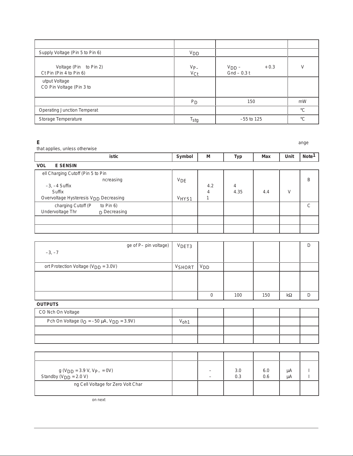
MARKING DIAGRAMS
1
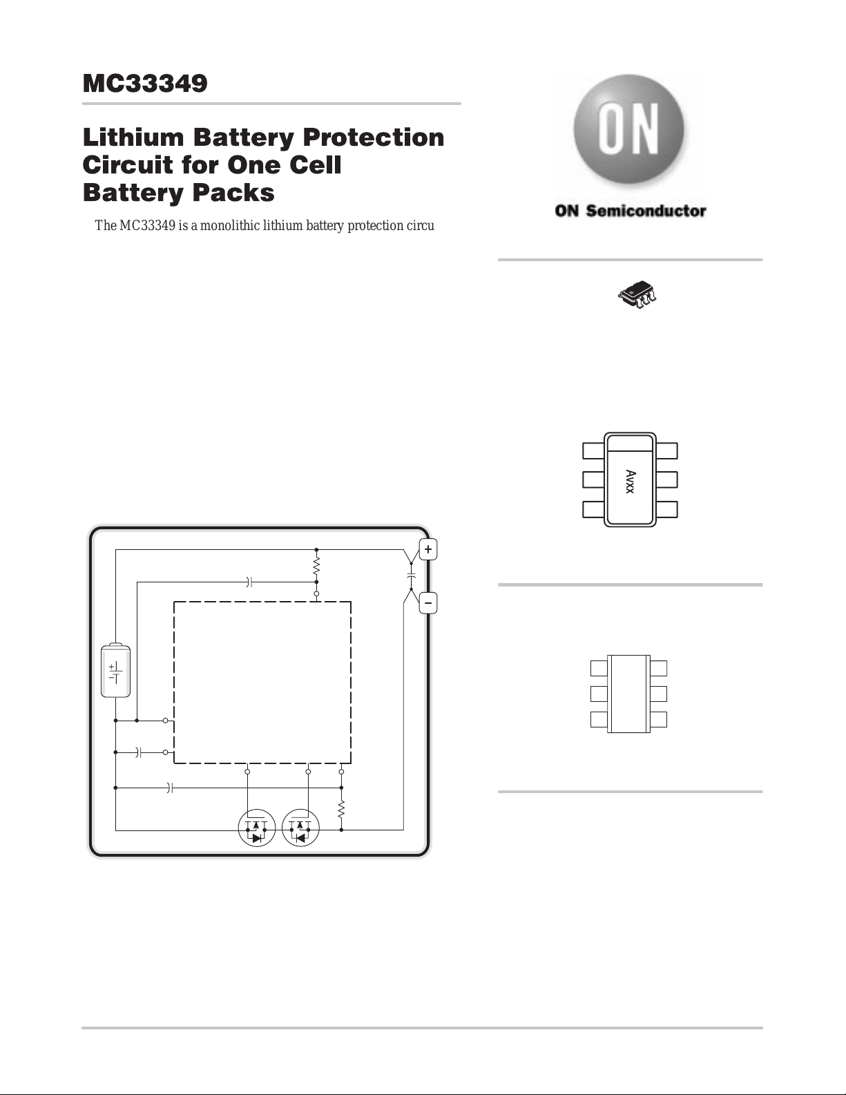
T ypical One Cell Smart Battery Pack
5
MC33349
6
4
132
v = Version code number
xx = Date code
PIN CONNECTIONS
16
DO
2
P–
CO
3
(Top View)
ORDERING INFORMATION
See detailed ordering and shipping information in the package
dimensions section on page 10 of this data sheet.
Gnd
5
V
cell
C
4
t
Semiconductor Components Industries, LLC, 2000
May, 2000 – Rev. 1
1 Publication Order Number:
MC33349/D

MC33349
Á
Á
Á
Á
MAXIMUM RATINGS
Characteristics Symbol Value Unit
Supply Voltage (Pin 5 to Pin 6)
Input Voltage
P– Pin Voltage (Pin 5 to Pin 2) V
Ct Pin (Pin 4 to Pin 6) V
Output Voltage
CO Pin Voltage (Pin 3 to Pin 2) V
DO Pin Voltage (Pin 1 to Pin 6) V
Power Dissipation
Operating Junction Temperature
Storage Temperature
БББББББББББББББ
ÁÁÁÁ
V
DD
P–
Ct
CO
DO
P
D
T
J
T
stg
БББББББ
–0.3 to 12
VDD – 28 to VDD + 0.3 V
Gnd – 0.3 to VDD + 0.3 V
VDD – 28 to VDD + 0.3 V
Gnd – 0.3 to VDD + 0.3 V
150
mW
–40 to 85
–55 to 125
ÁÁ
V
°C
°C
ELECTRICAL CHARACTERISTICS (C
= 0.01 µF, TA = 25°C, for min/max values TA is the operating junction temperature range
t
that applies, unless otherwise noted.)
Characteristic
Symbol Min Typ Max Unit Note
VOLTAGE SENSING
Cell Charging Cutoff (Pin 5 to Pin 6)
Overvoltage Threshold, VDD Increasing V
DET1
–3, –4 Suffix 4.2 4.25 4.3 V
–7 Suffix 4.3 4.35 4.4 V
Overvoltage Hysteresis VDD Decreasing V
HYS1
150 200 250 mV B
Cell Discharging Cutoff (Pin 5 to Pin 6)
Undervoltage Threshold, VDD Decreasing V
Overvoltage Delay Time (Ct = 0.01 µF, VDD = 3.6V to 4.5V) t
Undervoltage Delay Time (VDD = 3.6V to 2.4V) t
DET2
(DET1)
(DET2)
2.437 2.5 2.563 V
55 80 105 ms B
7.0 10 13 ms C
CURRENT SENSING
Excess Current Threshold (Detect rising edge of P– pin voltage)
V
DET3
–3, –7 Suffix 170 200 230 mV
–4 Suffix 45 75 105 mV
Short Protection Voltage (VDD = 3.0V)
V
SHORTVDD
– 1.1
VDD – 0.8
VDD – 0.5
V
Current Limit Delay Time (VDD = 3.0V)
Reset Resistance for Short Protection
t
(DET3)
t
(SHORT)
R
SHORT
9.0 13 17 ms D
– 5.0 50 µs D
50
100
150
k
W
OUTPUTS
CO Nch On Voltage (IO = 50 µA, VDD = 4.4V)
CO Pch On Voltage (IO = –50 µA, VDD = 3.9V)
DO Nch On Voltage (IO = 50 µA, VDD = 2.4V)
DO Pch On Voltage (IO = –50 µA, VDD = 3.9V)
V
V
V
V
ol1
oh1
ol2
oh2
3.4
3.4
–
–
0.2
3.8
0.2
3.7
0.5
0.5
V
–
V
V
–
V
TOTAL DEVICE
Operating Input Voltage
Supply Current
V
DD
I
cell
1.5
–
10
V
Operating (VDD = 3.9 V, VP– = 0V) – 3.0 6.0 µA I
Standby (VDD = 2.0 V) – 0.3 0.6 µA I
Minimum Operating Cell Voltage for Zero Volt Charging (Pin 5 to
Pin 2)
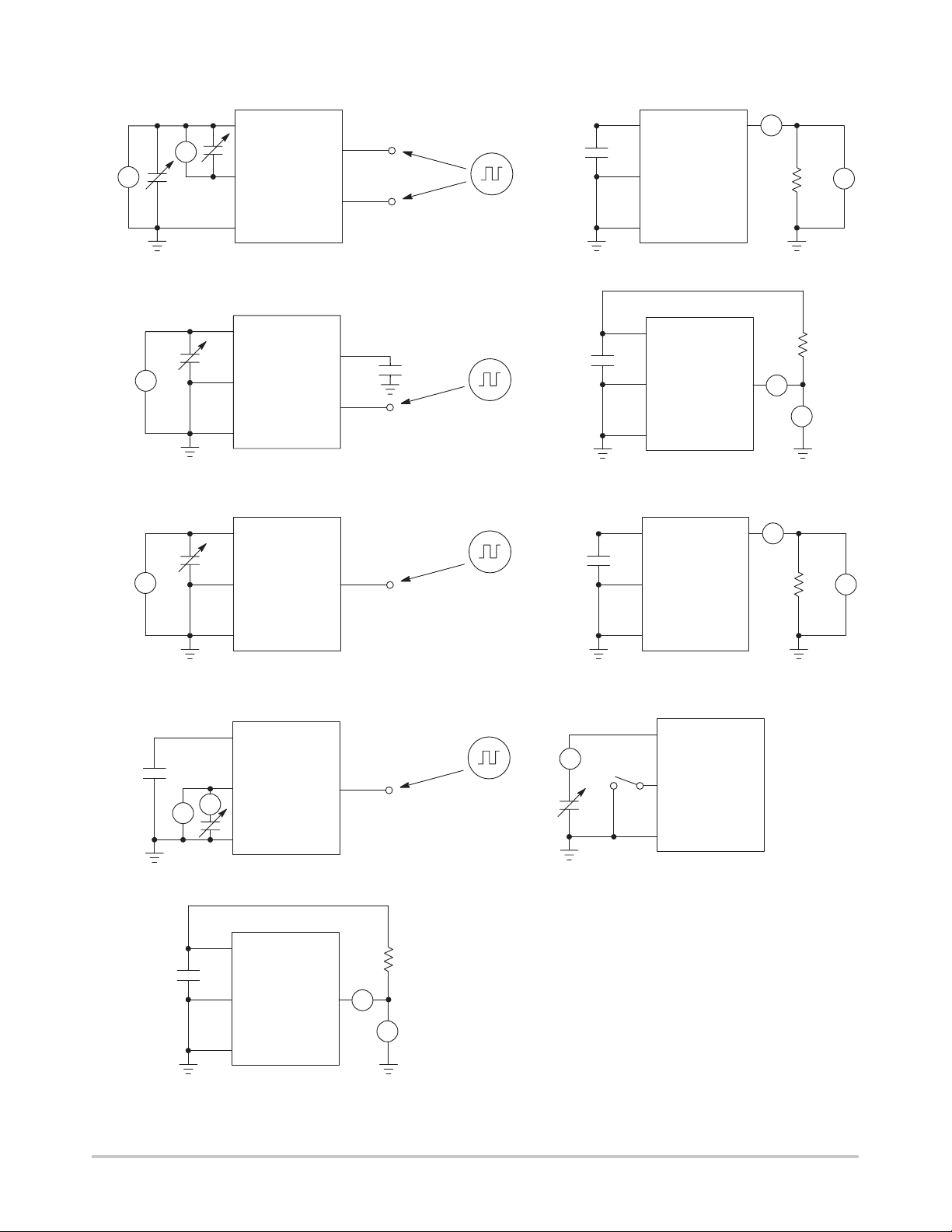
1. Indicates test circuits shown on next page.
V
ST
–
–
1.2
V
1
B
C
D
D
D
E
F
G
H
A
A
http://onsemi.com
2

MC33349
A
B
C
F
A
5
V
V
2
6
3
1
OSCILLOSCOPE
5
2
6
3
V
G
5
4
V
2
3
6
5
2
6
1
A
V
H
A
5
5
1
D
E
V
2
6
1
2
6
V
I
5
A
2
A
V
6
5
2
6
1
3
A
V
5
2
6
Figure 1. T est Circuit Schematics
http://onsemi.com
3

Vcell Ct
Á
Á
Á
Á
Á
Á
Á
Á
Á
5 4
VD1
VD2
VD3
MC33349
Level
Shift
Delay
10 kOhm
Short Circuit
Detector
Gnd Do Co P–
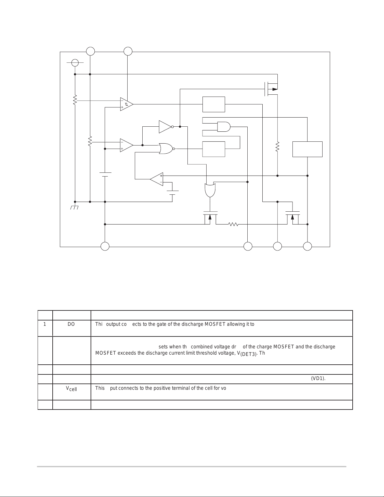
Figure 2. Detailed Block Diagram
PIN FUNCTION DESCRIPTION
Pin Symbol Description
1
2
Á
Á
3
4
5
Á
6
DO
P–
ÁÁÁ
ÁÁÁ
CO
C
t
V
cell
ÁÁÁ
Gnd
This output connects to the gate of the discharge MOSFET allowing it to enable or disable battery pack
discharging.
This pin monitors cell discharge current.
ББББББББББББББББББББББББББ
The excess current detector sets when the combined voltage drop of the charge MOSFET and the discharge
MOSFET exceeds the discharge current limit threshold voltage, V
ББББББББББББББББББББББББББ
V
is pulled within 0.8V of the cell voltage by a short circuit.
(P–)
This output connects to the gate of the charge MOSFET allowing it to enable or disable battery pack charging.
This pin connects to the external capacitor for setting the output delay of the overvoltage detector (VD1).
This input connects to the positive terminal of the cell for voltage monitoring and provides operating bias for the
ББББББББББББББББББББББББББ
integrated circuit.
This is the ground pin of the IC.
Rshort
1 3 26
. The short circuit detector activates when
(DET3)
http://onsemi.com
4
 Loading...