

Motorola MC33348D-6, MC33348D-4, MC33348D-5, MC33348D-3, MC33348D-1 Datasheet
...
The MC33348 is a monolithic lithium battery protection circuit that is
designed to enhance the useful operating life of a one cell rechargeable
battery pack. Cell protection features consist of internally trimmed charge
and discharge voltage limits, discharge current limit detection with a
delayed shutdown, and a virtually zero current sleepmode state when the
cell is discharged. An additional feature includes an on–chip charge pump
for reduced MOSFET losses while charging or discharging a low cell
voltage battery pack. This protection circuit requires a minimum number of
external components and is targeted for inclusion within the battery pack.
This MC33348 is available in standard SOIC 8 lead surface mount
package.
• Internally Trimmed Charge and Discharge Voltage Limits
• Discharge Current Limit Detection with Delayed Shutdown
• Virtually Zero Current Sleepmode State when Cells are Discharged
• Charge Pump for Reduced Losses with a Low Cell Voltage Battery Pack
• Dedicated for One Cell Applications
• Minimum Components for Inclusion within the Battery Pack
• Available in a Low Profile Surface Mount Package
Order this document by MC33348/D
LITHIUM BATTERY
PROTECTION CIRCUIT
FOR
ONE CELL
SMART BATTERY PACKS
SEMICONDUCTOR
TECHNICAL DATA
8
1
Ordering Information shown on following page.
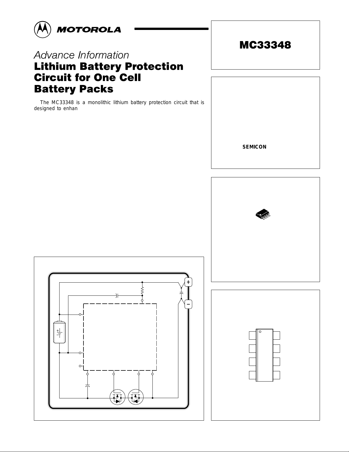
Typical One Cell Smart Battery Pack
Cell
Voltage
1
MC33348
Ground
3
T est
2
Charge Pump
8 Charge
Output
Discharge
Gate Drive
Output
4 6 5 Charge
Gate Drive
Output
7
V
CC
Gate Drive
Common/
Discharge
Current Limit
PLASTIC PACKAGE
PIN CONNECTIONS
Cell Voltage
Test
Ground
Discharge Gate
Drive Output
D SUFFIX
CASE 751
(SO–8)
18
2
3
4
(Top View)
Charge Pump
Output
V
7
CC
Charge Gate
6
Drive Output
Charge Gate Drive
5
Common/Discharge
Current Limit
This device contains 1170 active transistors.
This document contains information on a new product. Specifications and information herein
are subject to change without notice.
MOTOROLA ANALOG IC DEVICE DATA
Motorola, Inc. 1997 Rev 1
1
MC33348
4.20
2.25
4.25
300
2.28
T
25° to +85°C
SO–8
4.35
2.30
ORDERING INFORMATION
Charge
Overvoltage
Device
MC33348D–1
MC33348D–2
MC33348D–3
MC33348D–4
MC33348D–5
MC33348D–6
NOTE: Additional threshold limit options can be made available. Consult factory for information.
Threshold (V)
MAXIMUM RATINGS
Ratings Symbol Value Unit
Input Voltage (Measured with Respect to Ground, Pin 3)
Cell Voltage (Pin 1) 7.5
Test (Pin 2) 7.5
Discharge Gate Drive Output (Pin 4) 18
Charge Gate Drive Common/Discharge Current Limit (Pin 5) ±11
Charge Gate Drive Output (Pin 6) ±11
VCC (Pin 7) 7.5
Charge Pump Output (Pin 8) 10
Thermal Resistance, Junction–to–Air
D Suffix, SO–8 Plastic Package, Case 751 178
Operating Junction Temperature (Note 1)
Storage Temperature
NOTES: 1. Tested ambient temperature range for the MC33348:
T
= –25°CT
low
2.ESD data available upon request.
Charge
Overvoltage
Hysteresis (mV)
= +85°C
high
Discharge
Undervoltage
Threshold (V)
V
IR
R
θJA
T
J
T
stg
Discharge
Current Limit
Threshold (mV)
–40 to +150
–55 to +150
400
200
400
200
400
200
Operating
Temperature Range
–
= –
A
V
°C/W
°C
°C
Package
°
°
–
2
MOTOROLA ANALOG IC DEVICE DATA
MC33348
ÁÁÁÁ
ÁÁÁ
ÁÁÁÁ
ÁÁÁ
ÁÁÁÁ
ÁÁÁ
ÁÁÁÁ
ÁÁÁ
ÁÁÁÁ
ÁÁÁ
ÁÁÁÁ
ÁÁÁ
Á
ÁÁÁÁ
Á
Á
ÁÁÁ
Á
ÁÁÁÁ
ÁÁÁ
ELECTRICAL CHARACTERISTICS (V
= 4.0 V, TA = 25°C, for min/max values TA is the operating junction temperature range
CC
that applies (Note 1), unless otherwise noted.)
Characteristic
Symbol Min Typ Max Unit
VOLTAGE SENSING
Cell Charging Cutoff (Pin 1 to Pin 3)
Overvoltage Threshold, V
Increasing, TA = 25°C V
Cell
th(OV)
–1 Suffix 4.158 4.20 4.242
–2 Suffix 4.158 4.20 4.242
–3 Suffix 4.208 4.25 4.293
–4 Suffix 4.208 4.25 4.293
–5 Suffix 4.306 4.35 4.394
–6 Suffix 4.306 4.35 4.394
Overvoltage Hysteresis V
Decreasing V
Cell
H
–1 Suffix – 300 –
–2 Suffix – 300 –
–3 Suffix – 300 –
–4 Suffix – 300 –
–5 Suffix – 300 –
–6 Suffix – 300 –
Cell Discharging Cutoff (Pin 1 to Pin 3, TA = 25°C)
Undervoltage Threshold, V
Decreasing V
Cell
th(UV)
–1 Suffix 2.205 2.25 2.295
–2 Suffix 2.205 2.25 2.295
–3 Suffix 2.234 2.28 2.326
–4 Suffix 2.234 2.28 2.326
–5 Suffix 2.254 2.30 2.346
–6 Suffix 2.254 2.30 2.346
Input Bias Current During Cell Voltage Sample (Pin 1)
Cell Voltage Sampling Rate
I
IB
t
(smpl)
–
–
28
1.0
–
–
CURRENT SENSING
Discharge Current Limit (Pin 3 to Pin 5, TA = 25°C)
Threshold Voltage V
th(dschg)
–1 Suffix 360 400 440
–2 Suffix 180 200 220
–3 Suffix 360 400 440
–4 Suffix 180 200 220
–5 Suffix 360 400 440
–6 Suffix 180 200 220
Delay I
dly(dschg)
1.0 2.3 4.0 ms
CHARGE PUMP
Output Voltage (Pin 8, RL ≥ 1010, TA = 25°C)
V
O
8.0
10.2
12
TOTAL DEVICE
Average Cell Current (TA = 25°C, Battery Pack Unloaded and without
БББББББББББББББББ
Current Limit Fault)
I
CC
ÁÁÁ
ÁÁÁÁÁÁÁÁÁ
Operating (VCC = 4.0 V) – 17 20 µA
Sleepmode (VCC = 2.0 V) – 2.0 – nA
Minimum Operating Cell Voltage for Logic and Gate Drivers
NOTE: 1.Tested ambient temperature range for the MC33348:
T
= –25°CT
low
high
= +85°C
V
CC
–
1.5
–
V
mV
V
µA
s
mV
V
ÁÁ
V
MOTOROLA ANALOG IC DEVICE DATA
3
MC33348
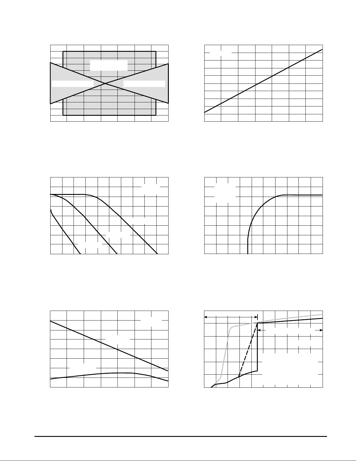
Figure 1. Charge and Discharge
Threshold V oltage Change versus Temperature
1.2
0.8
Maximum Threshold
0.4
0
Typical Threshold Change Typical Threshold Change
Charge Limits
–0.4
, THRESHOLD VOLTAGE CHANGE (%)
–0.8
–1.2
th(OV & UV)
V
∆
TA, AMBIENT TEMPERATURE (°C) TA, AMBIENT TEMPERATURE (°C)
Figure 3. Gate Drive Output Voltage
12
10
versus Load Current
CO = 10 nF
°
C
TA = 25
Figure 2. Discharge Current Limit
Threshold V oltage Change versus Temperature
16
VCC = 4.0 V
8.0
0
, CURRENT LIMIT THRESHOLD
–8.0
VOLTAGE CHANGE (%)
th(dschg)
–16
V
∆
1004020–20–40 0 60 80 1004020–20–40 0 60 80
Figure 4. Gate Drive Output Voltage
12
10
CO = 10 nF
Pin 2 = Gnd
RL ≥ 1010
TA = 25°C
versus Supply V oltage
Ω
8.0
6.0
, GATE DRIVE OUTPUT VOLTAGE (V)
O
V
4.0
12
11
10
9.0
, CHARGE PUMP OUTPUT VOL TAGE (V)
O
V
8.0
VCC = 4.15 V
VCC = 3.25 V
VCC = 2.35 V
IL, OUTPUT LOAD CURRENT (µA) VCC, SUPPLY VOLTAGE (V)
Figure 5. Charge Pump Output Voltage
versus T emperature
CO = 10 nF
≥
1010
RL
VCC = 4.15 V
In Regulation
VCC = 2.35 V
Out of Regulation
8.0
6.0
, GATE DRIVE OUTPUT VOLTAGE (V)
O
V
1.00.80.60.20 0.4
4.0
4.0
5.01.00 2.0 3.0
Figure 6. Supply Current
2
10
Battery Pack Sleepmode Range
1
Ω
1004020–20–40 0 60 80
10
µ
0
10
–1
10
–2
10
, SUPPLY CURRENT ( A)
CC
I
–3
10
–4
10
0 1.0 2.0 3.0 5.0
versus Supply V oltage
Battery Pack Operating Range
123
1 – Battery pack unloaded without
discharge current limit fault.
2 – Battery pack loaded without
discharge current limit fault.
3 – Battery pack loaded or unloaded
with discharge current limit fault.
VCC, SUPPLY VOLTAGE (V)TA, AMBIENT TEMPERATURE (°C)
TA = 25°C
4.0
4
MOTOROLA ANALOG IC DEVICE DATA
 Loading...