

Motorola MC33340P, MC33340D Datasheet
Order this document by MC33340/D
The MC33340 is a monolithic control IC that is specifically designed as a
fast charge controller for Nickel Cadmium (NiCd) and Nickel Metal Hydride
(NiMH) batteries. This device features negative slope voltage detection as
the primary means for fast charge termination. Accurate detection is ensured
by an output that momentarily interrupts the charge current for precise
voltage sampling. An additional secondary backup termination method can
be selected that consists of either a programmable time or temperature limit.
Protective features include battery over and undervoltage detection, latched
over temperature detection, and power supply input undervoltage lockout
with hysteresis. Provisions for entering a rapid test mode are available to
enhance end product testing. This device is available in an economical
8–lead surface mount package.
• Negative Slope Voltage Detection with 4.0 mV Sensitivity
• Accurate Zero Current Battery Voltage Sensing
• High Noise Immunity with Synchronous VFC/Logic
• Programmable 1 to 4 Hour Fast Charge Time Limit
• Programmable Over/Under Temperature Detection
• Battery Over and Undervoltage Fast Charge Protection
• Rapid System Test Mode
• Power Supply Input Undervoltage Lockout with Hysteresis
• Operating Voltage Range of 3.0 V to 18 V
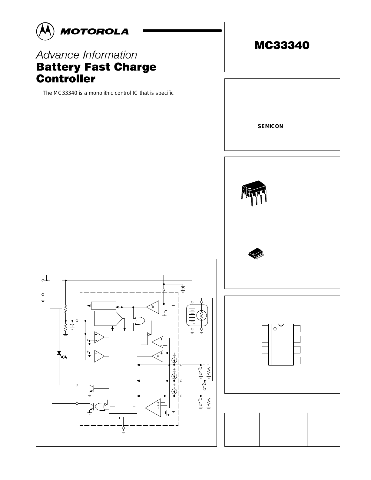
Simplified Block Diagram
BATTERY FAST CHARGE
CONTROLLER
SEMICONDUCTOR
TECHNICAL DATA
P SUFFIX
PLASTIC PACKAGE
8
1
8
1
CASE 626
D SUFFIX
PLASTIC PACKAGE
CASE 751
(SO–8)
DC
Input
∆
V Detect
Counter
Timer
Undervoltage
Lockout
Over
Under
t1
t2
t3
t/T
Time/
Temp
Select
4
R
Q
S
Regulator
Internal Bias
V
sen
1
V
sen
Gate
2
3
Fast/
Trickle
This device contains 2,512 active transistors.
This document contains information on a new product. Specifications and information herein
are subject to change without notice.
MOTOROLA ANALOG IC DEVICE DATA
Voltage to
Frequency
Converter
Ck F/V R
High
Battery
Detect
Low
V
Gate
F/T
–
sen
Gnd
V
Over
Temp
Latch
Temp
Detect
CC
8
V
CC
Battery
Pack
t1/T
High
ref
7
t2/T
sen
6
t3/T
Low
ref
5
V
CC
PIN CONNECTIONS
V
Input
sen
V
Gate Output
sen
Fast/Trickle Output
Gnd
1
2
3
4
(Top View)
8V
CC
t1/T
High
7
ref
6
t2/T
sen
5
t3/T
Low
ref
ORDERING INFORMATION
Operating
Device
MC33340D
MC33340P Plastic DIP
Motorola, Inc. 1996 Rev 0
Temperature Range
TA = –25° to +85°C
Package
SO–8
1
MC33340
Á
Á
Á
Á
Á
Á
Á
Á
Á
Á
Á
Á
MAXIMUM RATINGS
Rating Symbol Value Unit
Power Supply Voltage (Pin 8) V
CC
Input Voltage Range V
Time/Temperature Select (Pins 5, 6, 7) V
Battery Sense, Note 1 (Pin 1) V
V
Gate Output (Pin 2)
sen
Voltage
Current
IR(t/T)
IR(sen)
V
O(gate)
I
O(gate)
Fast/Trickle Output (Pin 3)
Voltage
Current
Thermal Resistance, Junction–to–Air R
V
O(F/T)
I
O(F/T)
θJA
P Suffix, DIP Plastic Package, Case 626 100
D Suffix, SO–8 Plastic Package, Case 751 178
Operating Junction Temperature T
Operating Ambient Temperature (Note 2) T
Storage Temperature T
NOTE: ESD data available upon request.
J
A
stg
18 V
–1.0 to V
CC
–1.0 to VCC + 0.6
or
–1.0 to 10
20
50
20
50
+150 °C
–25 to +85 °C
–55 to +150 °C
V
mA
V
mA
°C/W
ELECTRICAL CHARACTERISTICS (V
= 6.0 V, for typical values TA = 25°C, for min/max values TA is the operating
CC
ambient temperature range that applies (Note 2), unless otherwise noted.)
Characteristic
BATTERY SENSE INPUT (Pin 1)
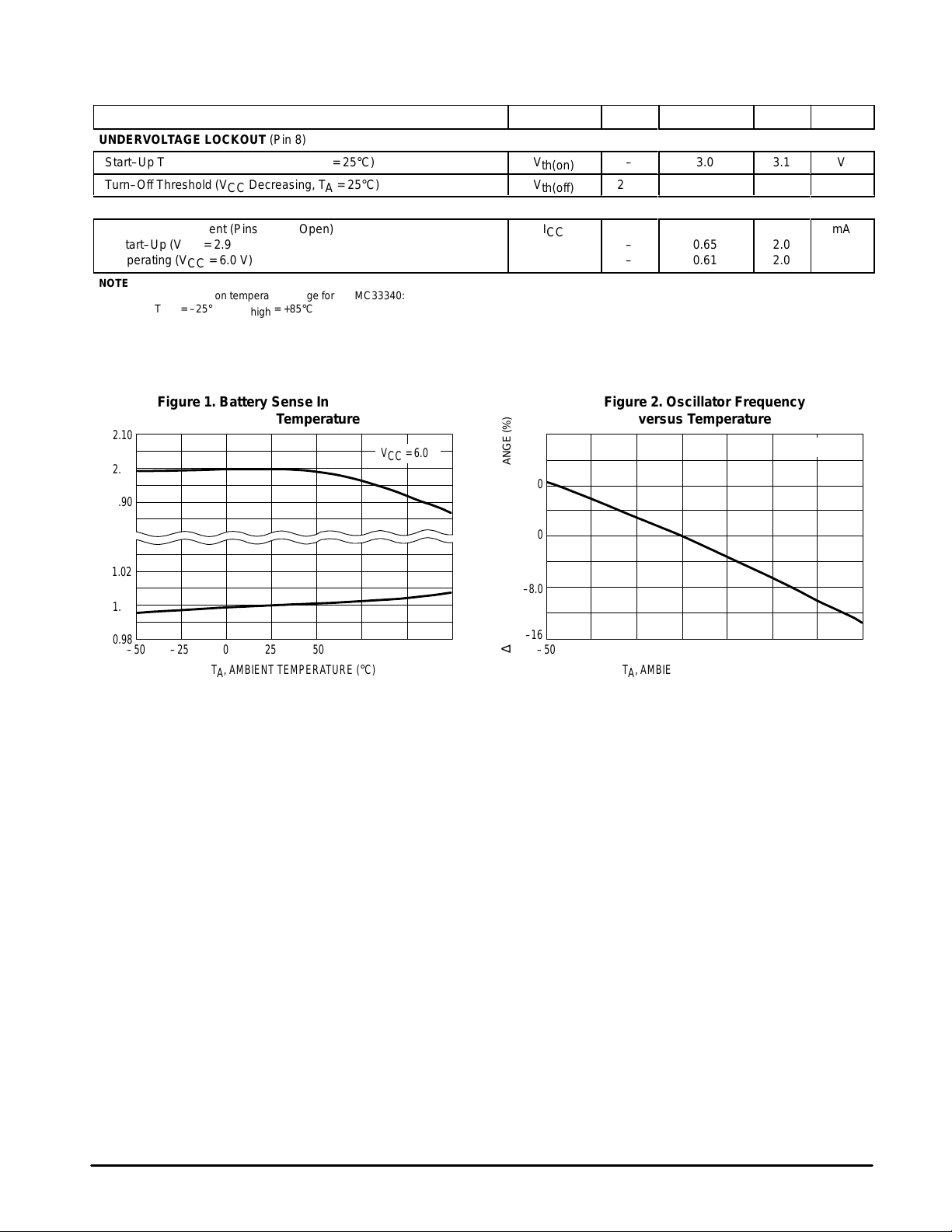
Input Sensitivity for –∆V Detection
Overvoltage Threshold
БББББББББББББББББ
Undervoltage Threshold
Input Bias Current
Input Resistance
TIME/TEMPERA TURE INPUTS (Pins 5, 6, 7)
Programing Inputs (Vin = 1.5 V)
БББББББББББББББББ
Input Current
Input Current Matching
БББББББББББББББББ
Input Offset Voltage, Over and Under Temperature Comparators
Under Temperature Comparator Hysteresis (Pin 5)
Temperature Select Threshold
INTERNAL TIMING
Internal Clock Oscillator Frequency
V
Gate Output (Pin 2)
sen
Gate Time
БББББББББББББББББ
Gate Repetition Rate
Fast Charge Holdoff from –∆V Detection
V
GATE OUTPUT (Pin 2)
sen
Off–State Leakage Current (VO = 20 V)
Low State Saturation Voltage (I
sink
= 10 mA)
FAST/TRICKLE OUTPUT (Pin 3)
Off–State Leakage Current (VO = 20 V)
Low State Saturation Voltage (I
NOTES: 1. Whichever voltage is lower.
2.Tested junction temperature range for the MC33340:
T
= –25°C T
low
high
= 10 mA)
sink
= +85°C
Symbol Min Typ Max Unit
–∆V
th
V
th(OV)
ÁÁÁ
V
th(UV)
I
IB
R
in
I
in
ÁÁÁ
∆I
in
ÁÁÁ
V
IO
V
H(T)
V
th(t/T)
f
OSC
t
gate
ÁÁÁ
t
hold
I
off
V
OL
I
off
V
OL
–
1.9
Á
0.95
–
–
Á
–24
–
Á
–
–
–
–
–
Á
–
–
–
–
–
–
–4.0
2.0
ÁÁÁ
1.0
10
6.0
ÁÁÁ
–30
1.0
ÁÁÁ
5.0
44
VCC –0.7
760
33
ÁÁÁ
1.38
177
10
1.2
10
1.0
2.1
Á
1.05
Á
–36
2.0
Á
Á
–
–
–
–
–
–
–
–
–
–
–
–
–
–
ÁÁ
ÁÁ
ÁÁ
ÁÁ
mV
V
mV
nA
MΩ
µA
%
mV
mV
mV
kHz
ms
s
s
nA
V
nA
V
2
MOTOROLA ANALOG IC DEVICE DATA
MC33340
Á
Á
Á
Á
Á
Á
ELECTRICAL CHARACTERISTICS (continued) (V
= 6.0 V, for typical values TA = 25°C, for min/max values TA is the operating
CC
ambient temperature range that applies (Note 2), unless otherwise noted.)
Characteristic UnitMaxTypMinSymbol
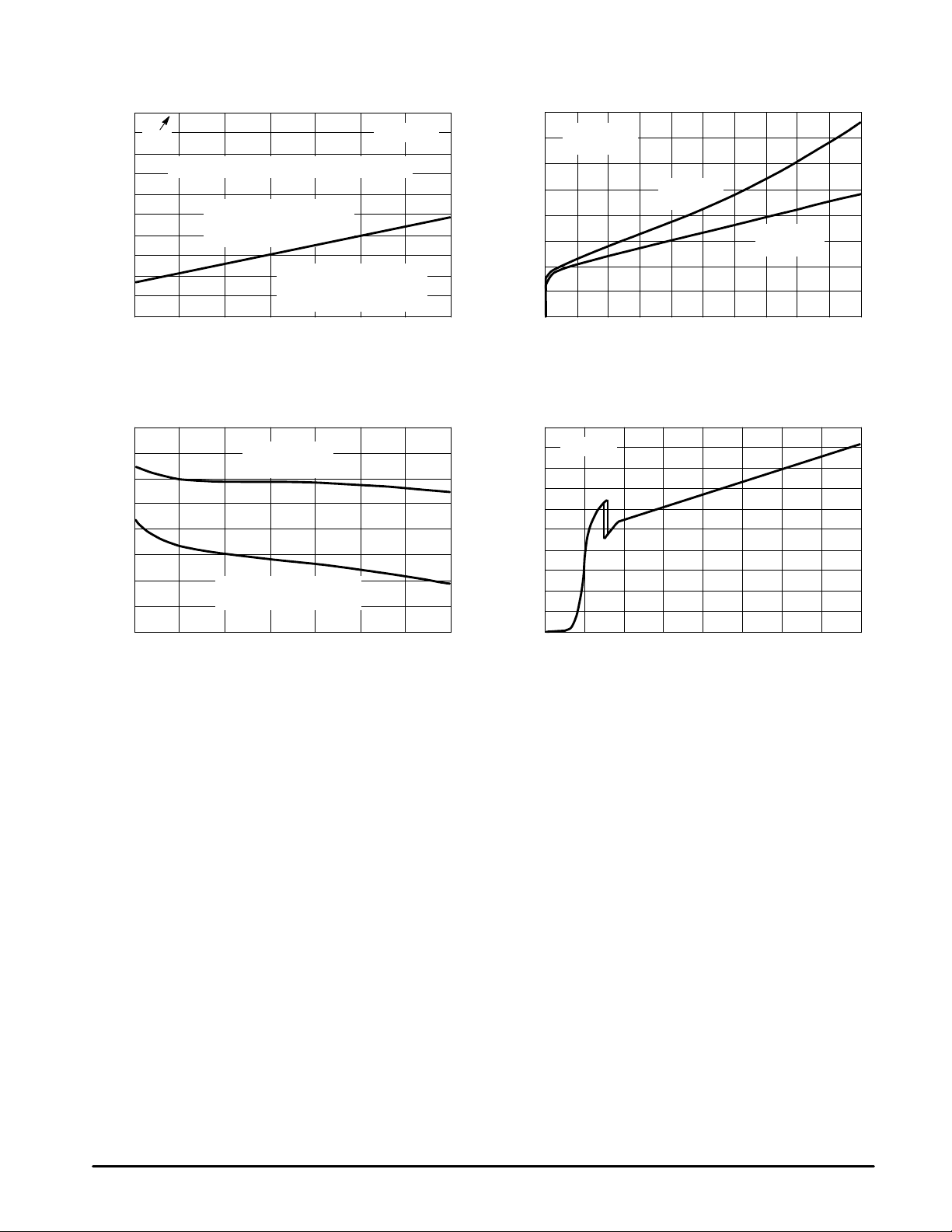
UNDERVOLTAGE LOCKOUT (Pin 8)
Start–Up Threshold (VCC Increasing, TA = 25°C)
Turn–Off Threshold (VCC Decreasing, TA = 25°C)
TOTAL DEVICE (Pin 8)
Power Supply Current (Pins 5, 6, 7 Open)
Start–Up (VCC = 2.9 V)
БББББББББББББББББ
Operating (VCC = 6.0 V)
NOTES: 1. Whichever voltage is lower.
2.Tested junction temperature range for the MC33340:
T
= –25°C T
low
high
= +85°C
Figure 1. Battery Sense Input Thresholds
versus T emperature
2.10
VCC = 6.0 V
2.00
1.90
V
th(on)
V
th(off)
I
CC
ÁÁÁ
16
8.0
–
2.75
–
Á
–
3.0
2.85
0.65
ÁÁÁ
0.61
3.1
2.0
Á
2.0
–
Figure 2. Oscillator Frequency
versus T emperature
VCC = 6.0 V
V
V
mA
ÁÁ
1.02
1.00
, OVER/UNDERVOL TAGE THRESHOLDS (V)
th
0.98
V
–50 –25 0 25 50 75 100 125
TA, AMBIENT TEMPERATURE (°C)
0
–8.0
, OSCILLAT OR FREQUENCY CHANGE (%)
–16
OSC
f
∆
–50 –25 0 25 50 75 100 125
TA, AMBIENT TEMPERATURE (°C)
MOTOROLA ANALOG IC DEVICE DATA
3
MC33340
V
Figure 3. T emperature Select Threshold Voltage
versus T emperature
0
V
CC
–0.2
0.4
–
–0.6
–0.8
, TEMPERATURE SELECT THRESHOLD VOLTAGE (
–1.0
th(t/T)
V
Threshold voltage is measured with respect to V
Time mode is selected if any of
the three inputs are above the
threshold.
Temperature mode is selected
when all three inputs are below
the threshold.
–50 –25 0 25 50 75 100 125
TA, AMBIENT TEMPERATURE (°C)
VCC = 6.0 V
CC
Figure 5. Undervoltage Lockout Thresholds
versus T emperature
3.1
Startup Threshold
3.0
2.9
, SUPPLY VOLTAGE (V)
2.8
CC
V
(VCC Increasing)
Minimum Operating Threshold
(VCC Decreasing)
Figure 4. Saturation V oltage versus Sink Current
V
Gate and Fast/Trickle Outputs
3.2
.
2.4
1.6
0.8
, SINK SATURATION VOLTAGE (V)
OL
V
0
0 8.0 16 24 32 40
sen
VCC = 6.0 V
°
C
TA = 25
V
Gate
sen
Pin 2
I
, SINK SATURATION (mA)
sink
Fast/Trickle
Pin 3
Figure 6. Supply Current
versus Supply V oltage
1.0
TA = 25°C
0.8
0.6
0.4
, SUPPLY CURRENT (mA)
0.2
CC
I
2.7
–50
–25 0 25 50 75 100 125
TA, AMBIENT TEMPERATURE (°C)
0
0 4.0 8.0 12 16
VCC, SUPPLY VOLTAGE (V)
INTRODUCTION
Nickel Cadmium and Nickel Metal Hydride batteries
require precise charge termination control to maximize cell
capacity and operating time while preventing overcharging.
Overcharging can result in a reduction of battery life as well
as physical harm to the end user. Since most portable
applications require the batteries to be charged rapidly, a
primary and usually a secondary or redundant charge
sensing technique is employed into the charging system. It is
also desirable to disable rapid charging if the battery voltage
or temperature is either too high or too low. In order to
address these issues, an economical and flexible fast charge
controller was developed.
The MC33340 contains many of the building blocks and
protection features that are employed in modern high
performance battery charger controllers that are specifically
designed for Nickel Cadmium and Nickel Metal Hydride
batteries. The device is designed to interface with either
primary or secondary side regulators for easy implementation
of a complete charging system. A representative block
diagram in a typical charging application is shown in Figure 7.
The battery voltage is monitored by the V
input that
sen
internally connects to a voltage to frequency converter and
counter for detection of a negative slope in battery voltage. A
timer with three programming inputs is available to provide
backup charge termination. Alternatively , these inputs can be
used to monitor the battery pack temperature and to set the
over and under temperature limits also for backup charge
termination.
Two active low open collector outputs are provided to
interface this controller with the external charging circuit. The
first output furnishes a gating pulse that momentarily
interrupts the charge current. This allows an accurate
method of sampling the battery voltage by eliminating voltage
drops that are associated with high charge currents and
wiring resistances. Also, any noise voltages generated by the
charging circuitry are eliminated. The second output is
designed to switch the charging source between fast and
trickle modes based upon the results of voltage, time, or
temperature. These outputs normally connect directly to a
linear or switching regulator control circuit in non–isolated
primary or secondary side applications. Both outputs can be
used to drive optoisolators in primary side applications that
require galvanic isolation. Figure 8 shows the typical charge
characteristics for NiCd and NiMh batteries.
4
MOTOROLA ANALOG IC DEVICE DATA
 Loading...