

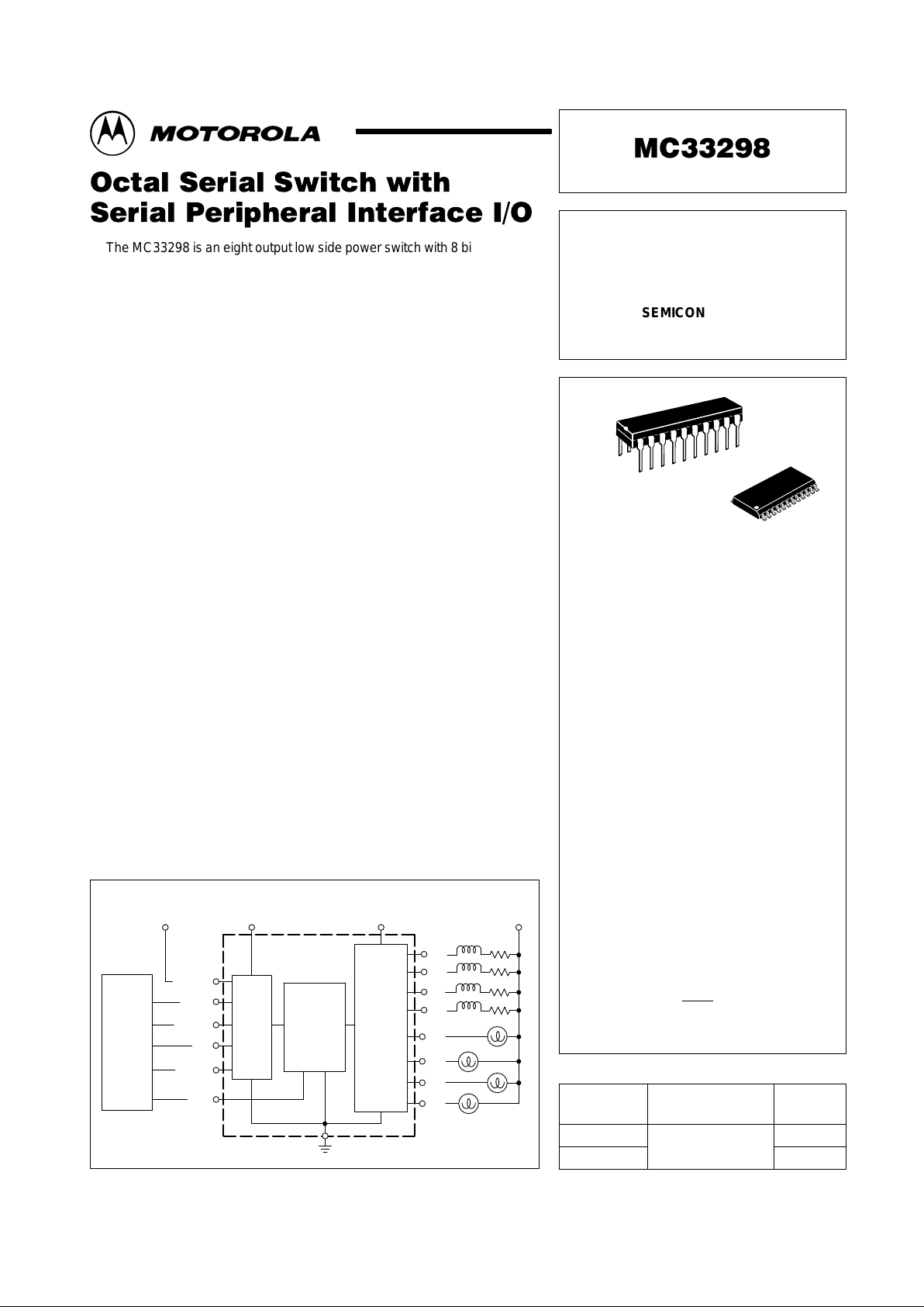
Motorola MC33298P, MC33298DW Datasheet
Device
Tested Operating
Temperature Range
Package
SEMICONDUCTOR
TECHNICAL DATA
OCTAL SERIAL SWITCH
(SPI Input/Output)
ORDERING INFORMATION
MC33298P
MC33298DW
TC = – 40° to +125°C
DIP
SOP–24L
Order this document by MC33298/D
P SUFFIX
PLASTIC PACKAGE
CASE 738
DIP (16+2+2)
PIN CONNECTIONS
20
1
DW SUFFIX
PLASTIC PACKAGE
CASE 751E
SOP (16+4+4)L
24
1
DIP Function SOP–24L
1
2
3
4
5
6
–
–
7
8
9
10
11
12
13
14
15
16
–
–
17
18
19
20
Output 7
Output 6
SCLK
SI
Ground
Ground
Ground
Ground
SO
CSB
Output 5
Output 4
Output 3
Output 2
SFPD
V
DD
Ground
Ground
Ground
Ground
V
PWR
Reset
Output 1
Output 0
1
2
3
4
5
6
7
8
9
10
11
12
13
14
15
16
17
18
19
20
21
22
23
24
1
MOTOROLA ANALOG IC DEVICE DATA
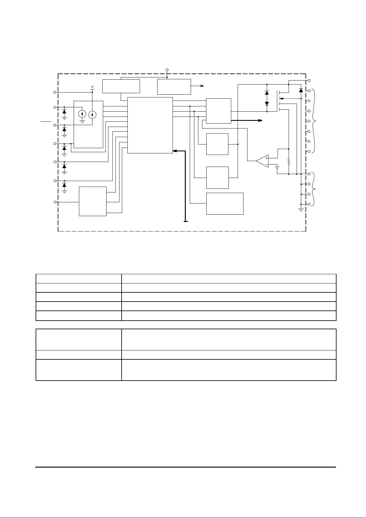
The MC33298 is an eight output low side power switch with 8 bit serial input
control. The MC33298 is a versatile circuit designed for automotive
applications, but is well suited for other environments. The MC33298
incorporates SMARTMOS technology, with CMOS logic, bipolar/MOS
analog circuitry, and DMOS power MOSFETs. The MC33298 interfaces
directly with a microcontroller to control various inductive or incandescent
loads. The circuit’s innovative monitoring and protection features are: very low
standby current, cascadable fault reporting, internal 65 V clamp on each
output, output specific diagnostics, and independent shutdown of outputs. The
MC33298 is parametrically specified over a temperature range of – 40°C ≤ T
A
≤ +125°C ambient temperature and 9.0 V ≤ V
PWR
≤ 16 V supply. The
economical 20 pin DIP and SO–24 wide body surface mount plastic packages
make the MC33298 very cost effective.
• Designed to Operate Over Wide Supply Voltages of 5.5 V to 26.5 V
• Interfaces Directly to Microprocessor Using SPI Protocol
• SPI Communication for Control and Fault Reporting
• 8–Bit Serial I/O is CMOS Compatible
• 3.0 A Peak Current Outputs with Maximum R
DS(on)
of 0.45 Ω at 25°C
• Outputs are Current Limited to 3.0 A to 6.0 A for Driving Incandescent
Lamp Loads
• Output Voltages Clamped to 65 V During Inductive Switching
• Maximum Sleep Current (I
PWR
) of 50 µA with VDD ≤ 2.0 V
• Maximum of 4.0 mA I
DD
During Operation
• Maximum of 2.0 mA I
PWR
During Operation with All Outputs “On”
• Open Load Detection (Outputs “Off”)
• Overvoltage Detection and Shutdown
• Each Output has Independent Over Temperature Detection and Shutdown
• Output Mode Programmable for Sustained Current Limit or Shutdown
• Short Circuit Detect and Shutdown with Automatic Retry for Every
Write Cycle
• Serial Operation Guaranteed to 2.0 MHz
Micro–
controller
with Bus
+V
bat
SCLK
CSB
SFPD
SO
V
PWR
V
DD
CMOS
Serial Shift
Registers
and
Latches
CMOS
Input
Logic
Updrain
DMOS
Output
Switches
and
Sense
Circuits
SI
Reset
SFPD
Y
0
Y
1
Y
2
Y
3
Y
4
Y
5
Y
6
Y
7
Gnd
This device contains 1,200 active transistors.
Simplified Application
Motorola, Inc. 1996 Rev 2
MC33298
2
MOTOROLA ANALOG IC DEVICE DATA
I
Limit
Output 0
R
S
Open
Load
Detect
Short
Circuit
Detect
Over
Temperature
Detect
SO
SI
SCLK
CSB
Reset
SFPD
V
DD
Gate
Control
65 V
Outputs
1–7
Grounds
Figure 1. Simplified Block Diagram
Overvoltage
Detect
Voltage
Regulator
Fault
Timers
OVD
RB
SFPDB
SFL
CSB
SCLK
SI
SO
CSI
CSBI
To Gates
1–7
From Detectors 1 to 7
V
PWR
Serial D/O
Line Driver
SPI
Interface
Logic
GE
OT
SF
OF
20
µ
A
20
µ
A
Bias
FAULT OPERATION
SERIAL OUTPUT (SO) PIN REPORTS
Overvoltage
Overvoltage condition reported.
Over Temperature Fault reported by Serial Output (SO) pin.
Over Current SO pin reports short to battery/supply or over current condition.
Output “On,” Open Load Fault Not reported.
Output “Off,” Open Load Fault SO pin reports output “off” open load condition.
DEVICE SHUTDOWNS
Overvoltage Total device shutdown at V
PWR
= 28–36 V. Re–operates when overvoltage is removed with
all outputs assuming an off state upon recovery from overvoltage. All device registers are
automatically reset (cleared) during shutdown.
Over Temperature Only the output experiencing an over temperature shuts down.
Over Current Only the output experiencing an over current condition shuts down at 3.0 A to 6.0 A after a
25 µs to 100 µs delay, with SFPD pin grounded. All outputs will continue to operate in a current
limit mode, with no shutdown, if the SPFD pin is at 5.0 V.
MC33298
3
MOTOROLA ANALOG IC DEVICE DATA
MAXIMUM RATINGS (All voltages are with respect to ground, unless otherwise noted.)
Rating Symbol Value Unit
Power Supply Voltage
Steady–State V
PWR(sus)
–1.5 to 26.5 V
Transient Conditions (Note1) V
PWR(pk)
–13 to 60 V
Logic Supply Voltage (Note 2) V
DD
– 0.3 to 7.0 V
Input Pin Voltage (Note 3) V
IN
– 0.3 to 7.0 V
Output Clamp Voltage (Note 4) V
OUT(off)
V
(2.0 mA ≤ I
out
≤ 0.5 A) 50 to 75
Output Self–Limit Current I
OUT(lim)
3.0 to 6.0 A
Continuous Per Output Current (Note 5) I
OUT(cont)
1.0 A
ESD Voltage
Human Body Model (Note 6) V
ESD1
2000 V
Machine Model (Note 7) V
ESD2
200 V
Output Clamp Energy (Note 8) E
clamp
Repetitive:
TJ =25°C 100 mJ
TJ = 125°C 30 mJ
Non–Repetitive:
TJ =25°C 2.0 J
TJ = 125°C 0.5 J
Recommended Frequency of SPI Operation (Note 9) f
SPI
2.0 MHz
Storage Temperature T
stg
– 55 to +150 °C
Operating Case Temperature T
C
– 40 to +125 °C
Operating Junction Temperature T
J
– 40 to +150 °C
Power Dissipation (TA =25°C) (Note 10) P
D
3.0 W
Soldering Temperature (for 10 seconds) T
solder
260 °C
Thermal Resistance, Junction–to–Ambient (Note 11) R
θJA
°C/W
Plastic Package, Case 738:
All Outputs “On” (Note 12) 31
Single Output “On” (Note 13) 37
SOP–24 Package, Case 751E:
All Outputs “On” (Note 12) 34
Single Output (Note 13) 40
NOTES: 1. Transient capability with external 100 Ω resistor connected in series with V
PWR
pin and supply.
2. Exceeding these limits may cause a malfunction or permanent damage to the device.
3. Exceeding voltage limits on SCLK, SI, CSB, SFPD, or Reset pins may cause permanent damage to
the device.
4. With output “off.”
5. Continuous output rating so long as maximum junction temperature is not exceeded. (See Figure 21 and
22 for more details).
6. ESD1 testing is performed in accordance with the Human Body Model (C
Zap
= 100 pF, R
Zap
= 1500 Ω).
7. ESD2 testing is performed in accordance with the Machine Model (C
Zap
= 100 pF, R
Zap
= 0 Ω).
8. Maximum output clamp energy capability at indicated Junction Temperature using single pulse method.
See Figure 19 for more details.
9. Guaranteed and production tested for 2.0 MHz SPI operation but has been demonstrated to operate to
8.5 MHz @ 25°C.
10. Maximum power dissipation at indicated junction temperature with no heat sink used. See Figures 20,
21, and 22 for more details.
11. See Figure 20 for Thermal Model.
12. Thermal resistance from Junction–to–Ambient with all outputs “on” and dissipating equal power.
13. Thermal resistance from Junction–to–Ambient with a single output “on.”
MC33298
4
MOTOROLA ANALOG IC DEVICE DATA
STATIC ELECTRICAL CHARACTERISTICS
(Characteristics noted under conditions of 4.5 V ≤ VDD ≤ 5.5 V, 9.0 V ≤V
PWR
≤ 16 V,
–40°C ≤ TC ≤ 125°C, unless otherwise noted.)
Characteristic
Symbol Min Typ Max Unit
POWER INPUT
Supply Voltage Range V
Quasi–Functional (Note 1) V
PWR(qf)
5.5 – 9.0
Full Operational V
PWR(fo)
9.0 – 26.5
Supply Current (all Outputs “On,” I
out
= 0.5 A) (Note 2) I
PWR(on)
– 1.0 2.0 mA
Sleep State Supply Current (VDD
=0.5 V)
I
PWR(ss)
– 1.0 50 µA
Sleep State Output Leakage Current (per Output, VDD = 0.5 V) I
OUT(ss)
– – 50 µA
Overvoltage Shutdown V
OV
28 – 36 V
Overvoltage Shutdown Hysteresis V
OV(hys)
0.2 – 1.5 V
Logic Supply Voltage V
DD
4.5 – 5.5 V
Logic Supply Current (with any combination of Outputs “On”) I
DD
– – 4.0 mA
Logic Supply Undervoltage Lockout Threshold (Note 3) V
DD(uvlo)
2.0 – 4.5 V
POWER OUTPUT
Drain–to–Source “On” Resistance (I
out
= 0.5 A, TJ =25°C) R
DS(on)
Ω
V
PWR
= 5.5 V – – 1.0
V
PWR
= 9.0 V – 0.4 0.5
V
PWR
= 13 V – 0.35 0.45
Drain–to–Source “On” Resistance (I
out
= 0.5 A, TJ = 150°C) R
DS(on)
Ω
V
PWR
= 5.5 V – – 1.8
V
PWR
= 9.0 V – 0.75 0.9
V
PWR
= 13 V – 0.65 0.8
Output Self–Limiting Current I
OUT(lim)
A
Outputs Programmed “On”, V
out
= 0.6 V
DD
3.0 4.0 6.0
Output Fault Detect Threshold (Note 4) V
OUTth(F)
V
DD
Output Programmed “Off” 0.6 0.7 0.8
Output “Off” Open Load Detect Current (Note 5) I
OCO
µA
Output Programmed “Off,” V
out
= 0.6 V
DD
30 50 100
Output Clamp Voltage V
OK
V
2.0 mA ≤ I
out
≤ 200 mA 50 60 75
Output Leakage Current (VDD ≤ 2.0 V) (Note 6) I
OUT(lkg)
–50 0 50 µA
Over T emperature Shutdown (Outputs “Of f”) (Note 7) T
LIM
155 170 185 °C
Over Temperature Shutdown Hysteresis (Note 7) T
LIM(hys)
– 10 20 °C
NOTES: 1. SPI inputs and outputs operational; Fault reporting may not be fully operational within this voltage range.
2.Value reflects normal operation (no faults) with all outputs “on.” Each “on” output contributes approximately 20 µA to I
PWR
. Each output experiencing
a “soft short” condition contributes approximately 0.5 mA to I
PWR
. A “soft short” is defined as any load current causing the output source current to
self–limit. A “hard” output short is a very low impedance short to supply.
3.For VDD less than the Undervoltage Lockout Threshold voltage, all data registers are reset and all outputs are disabled.
4.Output fault detect threshold with outputs programmed “off.” Output fault detect thresholds are the same for output opens and shorts.
5.Output “Off” Open Load Detect Current is the current required to flow through the load for the purpose of detecting the existence of an open condition
when the specific output is commanded to be “off.”
6.Output leakage current measured with output “off” and at 16 V.
7.This parameter is guaranteed by design but is not production tested.
MC33298
5
MOTOROLA ANALOG IC DEVICE DATA
STATIC ELECTRICAL CHARACTERISTICS (Characteristics noted under conditions of 4.5 V ≤ V
DD
≤ 5.5 V, 9.0 V ≤ V
PWR
≤ 16 V ,
–40°C ≤ TC ≤ 125°C, unless otherwise noted.)
Characteristic
Symbol Min Typ Max Unit
DIGITAL INTERFACE
Input Logic High Voltage (Note 1) V
IH
0.7 – 1.0 V
DD
Input Logic Low Voltage (Note 2) V
IL
0.0 – 0.2 V
DD
Input Logic Voltage Hysteresis (Note 3) V
I(hys)
50 100 500 mV
Input Logic Current (Note 4) I
IN
–10 0 10 µA
Reset Pull–Up Current (Reset = 0.7 V
DD)
I
RSTB
10 22 50 µA
SFPD Pull–Down Current (SFPD = 0.2 VDD) I
SFPD
10 22 50 µA
SO High State Output Voltage (IOH = 1.0 mA) V
SOH
V
DD
–1.0 V V
DD
– 0.6 V – V
SO Low State Output Voltage (IOL = –1.6 mA) V
SOL
– 0.2 0.4 V
SO Tri–State Leakage Current (CSB = 0.7 VDD, 0 V ≤ VSO ≤ VDD) I
SOT
–10 0 10 µA
Input Capacitance (0 V ≤ VDD ≤ 5.5 V) (Note 5) C
IN
– – 12 pF
SO Tri–State Capacitance (0 V ≤ VDD ≤ 5.5 V) (Note 6) C
SOT
– – 20 pF
NOTES: 1. Upper logic threshold voltage range applies to SI, CSB, SCLK, Reset, and SFPD input signals.
2.Lower logic threshold voltage range applies to SI, CSB, SCLK, Reset, and SFPD input signals.
3.Only the SFPD and Reset inputs have hysteresis. This parameter is guaranteed by design but is not production tested.
4.Input current of SCLK, SI, and CSB logic control inputs.
5.Input capacitance of SI, CSB, SCLK, Reset, and SFPD for 0 V ≤ VDD ≤ 5.5 V. This parameter is guaranteed by design, but is not production tested.
6.Tri–state capacitance of SO for 0 V ≤ VDD ≤ 5.5 V. This parameter is guaranteed by design but is not production tested.
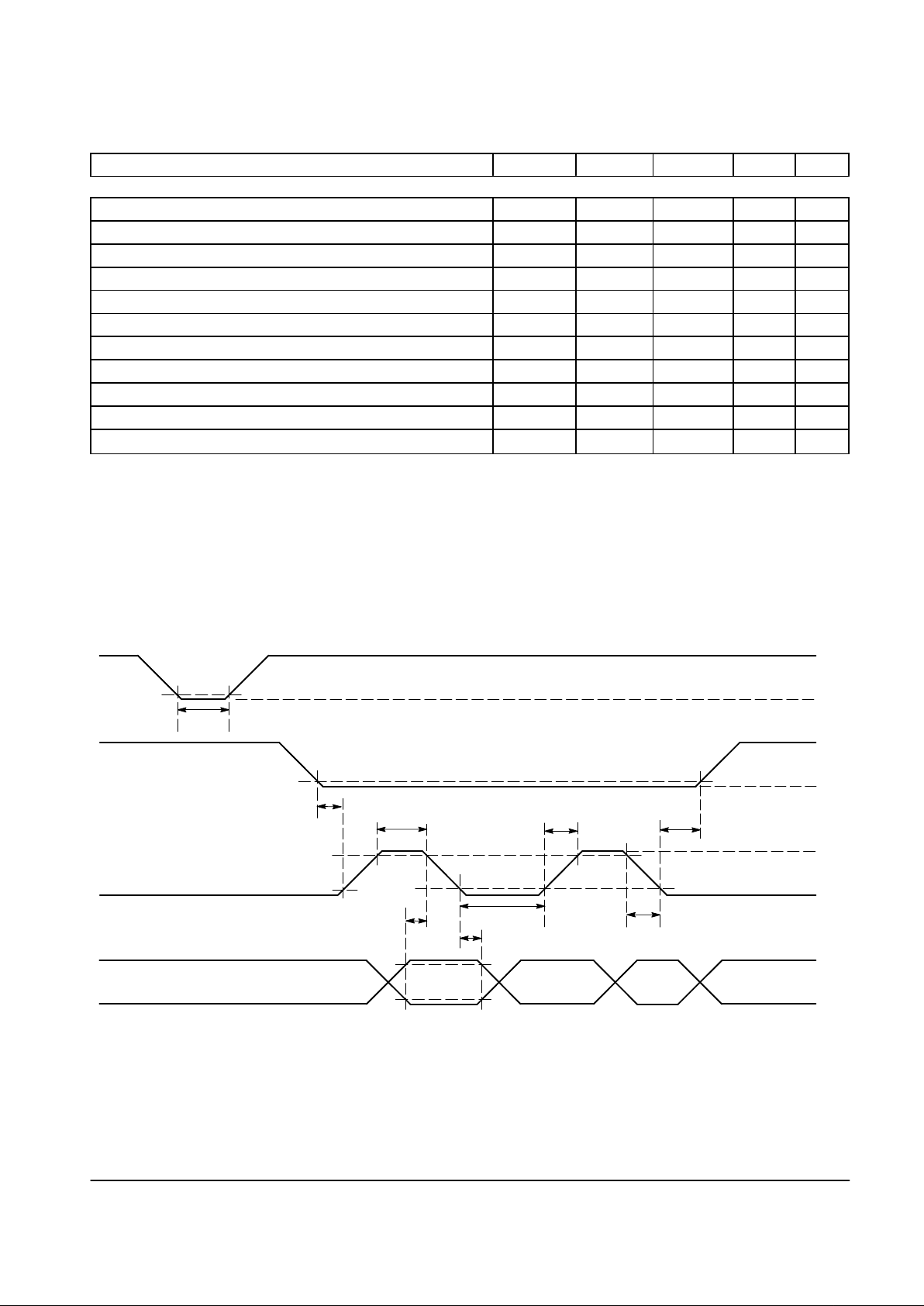
V
IH
V
IL
Don’t Care
0.2 V
DD
0.7 V
DD
t
lag
t
r
t
f
SI
t
wSCLKL
t
SI(hold)
t
SISU
Valid
t
wSCLKH
0.7 V
DD
0.2 V
DD
t
lead
SCLK
0.2 V
DD
0.2 V
DD
t
wRSTB
RSTB
CSB
Don’t Care Don’t CareValid
V
IH
V
IL
V
IH
V
IL
V
IH
V
IL
Figure 2. Input Timing Switch Characteristics
MC33298
6
MOTOROLA ANALOG IC DEVICE DATA
DYNAMIC ELECTRICAL CHARACTERISTICS
(Characteristics noted under conditions of 4.5 V ≤ VDD ≤ 5.5 V,
9.0 V ≤ V
PWR
≤ 16 V, – 40°C ≤ TC ≤ 125°C, unless otherwise noted.)
Characteristic
Symbol Min Typ Max Unit
POWER OUTPUT TIMING
Output Rise Time (V
PWR
= 13 V, RL = 26 Ω) (Note 1) t
r
0.4 1.5 20 µs
Output Fall Time (V
PWR
= 13 V, RL = 26 Ω) (Note 1) t
f
0.4 2.5 20 µs
Output Turn “On” Delay Time (V
PWR
= 13 V, RL = 26 Ω) (Note 2) t
dly(on)
1.0 5.0 15 µs
Output Turn “Off” Delay Time (V
PWR
= 13 V, RL = 26 Ω) (Note 3) t
dly(off)
1.0 5.0 15 µs
Output Short Fault Disable Report Delay (Note 4) t
dly(sf)
µs
SFPD = 0.2 x V
DD
25 50 100
Output “Off” Fault Report Delay (Note 5) t
dly(off)
µs
SFPD = 0.2 x V
DD
25 50 100
NOTES: 1. Output Rise and Fall time respectively measured across a 26 Ω resistive load at 10% to 90% and 90% to 10% voltage points.
2.Output Turn “On” Delay time measured from rising edge of CSB to 50% of output “off” V
out
voltage with RL = 26 Ω resistive load
(see Figure 7 and 9).
3.Output Turn “Off” Delay time measured from rising edge of CSB to 50% of output “off” V
out
voltage with RL = 26 Ω resistive load
(see Figure 7 and 9).
4.Output Short Fault Disable Report Delay measured from rising edge of CSB to I
out
= 2.0 A point with output “on,” V
out
= 5.0 V,
and SFPD = 0.2 x VDD (see Figure 8 and 10).
5.Output “Off” Fault Report Delay measured from 50% points of rising edge of CSB to rising edge of output (see Figure 9).
DYNAMIC ELECTRICAL CHARACTERISTICS (Characteristics noted under conditions of 4.5 V ≤ V
DD
≤ 5.5 V,
9.0 V ≤ V
PWR
≤ 16 V , –40°C ≤ TC ≤ 125°C, unless otherwise noted.)
Characteristic Symbol Min Typ Max Unit
DIGITAL INTERFACE TIMING
SCLK Clock Period (Note 6) t
pSCLK
500 – – ns
SCLK Clock High Time t
wSCLKH
175 – – ns
SCLK Clock Low Time t
wSCLKL
175 – – ns
Required Low State Duration for Reset (VIL ≤ 0.2 VDD) (Note 1) t
wRSTB
250 50 – ns
Falling Edge of CSB to Rising Edge of SCLK (Required Setup Time) t
lead
250 50 – ns
Falling Edge of SCLK to Rising Edge of CSB (Required Setup Time) t
lag
250 50 – ns
SI to Falling Edge of SCLK (Required Setup Time) t
SISU
125 25 – ns
Falling Edge of SCLK to SI (Required Hold Time) t
SI(hold)
125 25 – ns
SO Rise Time (CL = 200 pF) t
rSO
– 25 75 ns
SO Fall Time (CL = 200 pF) t
fSO
– 25 75 ns
SI, CSB, SCLK Incoming Signal Rise Time (Note 2) t
rSI
– – 200 ns
SI, CSB, SCLK Incoming Signal Fall TIme (Note 2) t
fSI
– – 200 ns
Time from Falling Edge of CSB to SO ns
Low Impedance (Note 3) t
SO(en)
– – 200
HIgh Impedance (Note 4) t
SO(dis)
– – 200
Time from Rising Edge of SCLK to SO Data Valid (Note 5) t
valid
0.2 VDD ≤ SO ≥ 0.8 VDD, CL = 200 pF – 50 125 ns
NOTES: 1. Reset Low duration measured with outputs enabled and going to “off” or disabled condition.
2. Rise and Fall time of incoming SI, CSB, and SCLK signals suggested for design consideration to prevent the occurrence of double pulsing.
3.Time required for output status data to be available for use at SO.
4.Time required for output status data to be terminated at SO.
5.Time required to obtain valid data out from SO following the rise of SCLK.
6.Clock period includes 75 ns rise plus 75 ns fall transition time in addition to clock high and low time.
MC33298
7
MOTOROLA ANALOG IC DEVICE DATA
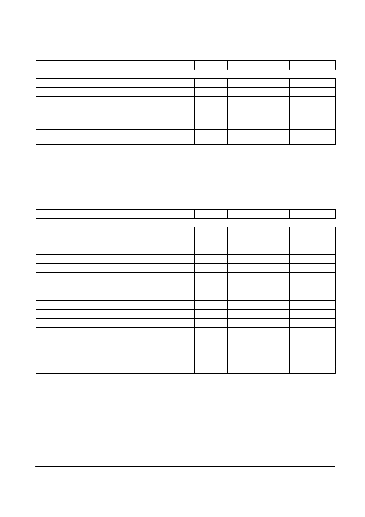
(Low–to–High)
SO
CL = 200 pF
VDD = 5.0 V
SCLK
MC33298
Under
Test
CL represents the total capacitance of the test fixture and probe.
t
fSI
t
rSI
0.2 V
DD
0.7 V
DD
0.2 V
DD
0.7 V
DD
t
fSO
t
valid
t
rSO
V
OL
V
OH
V
OL
V
OH
t
dly(hl)
t
dly(lh)
0.2 V
DD
0.7 VDD (2.5 V)
0
5.0 V
≤
10 ns
50%
≤
10 ns
SO (low–to–high) is for an output with internal conditions such that
the low–to–high transition of CSB causes the SO output to switch
from high–to–low.
SO
CL = 20 pF
RL = 2.0 k
Ω
V
Pull–Up
= 2.5 V
VDD = 5.0 V
CSB
MC33298
Under
Test
CL represents the total capacitance of the test fixture and probe.
t
rSI
t
fSI
V
OL
V
OH
V
OL
V
OH
0
5.0 V
SO
t
SO(dis)
t
SO(en)
t
SO(dis)
t
SO(en)
(High–to–Low)
0.7 V
DD
0.2 VDD (2.5 V)
≤
10 ns
≤
10 ns
CSB
NOTES: 1. SO (high–to–low) waveform is for SO output with internal
conditions such that SO output is low except when an output is
disabled as a result of detecting a circuit fault with CSB in a
High Logic state (e.g., open load).
2.SO (low–to–high) waveform is for SO output with internal
conditions such that SO output is high except when an output
is disabled as a result of detecting a circuit fault with CSB in
a High Logic state (e.g., shorted load).
50%
50%
90%
SO
(Low–to–High)
SO
SCLK
(High–to–Low)
SO
50%
10%
Figure 3. Valid Data Delay Time and
Valid Time Test Circuit
Figure 4. Enable and Disable Time Test Circuit
Figure 5. Vaild Data Delay Time and
Valid Time Waveforms
Figure 6. Enable and Disable Time Waveforms
MC33298
8
MOTOROLA ANALOG IC DEVICE DATA
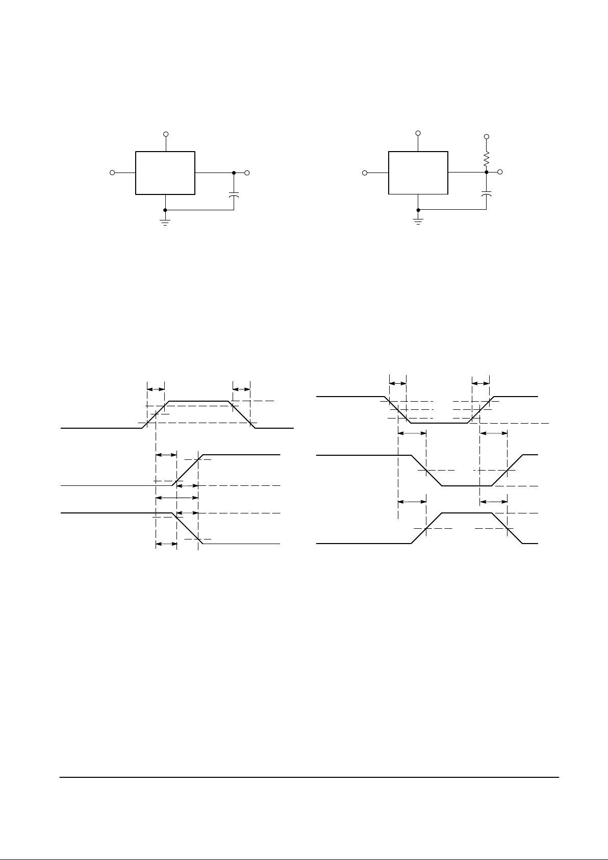
Output
C
L
RL = 26
Ω
V
PWR
= 14 V
VDD = 5.0 V
CSB
MC33298
Under
Test
CL represents the total capacitance of the test fixture and probe.
t
fSI
t
rSI
V
OL
14 V
V
OL
14 V
0
5.0 V
t
dly(on)
50%
Output Voltage
Waveform 2
≤
10 ns
50% 10%
90%
≤
10 ns
90%
50%
10%
CSB
t
dly(off)
50%
Output Voltage
Waveform 1
NOTES: 1. t
dly(on)
and t
dly(off)
are turn–on and turn–off propagation
delay times.
2.Waveform 1 is an output programmed from an “on” to an
“off” state.
3. Waveform 2 is an output programmed from an “off” to an
“on” state.
Output
CL = 20 pF
IL = 2.0 A
(Output “On”)
V
PWR
= 11 V
VDD = 5.0 V
CSB
MC33298
Under
Test
CL represents the total capacitance of the test fixture and probe.
t
fSI
t
rSI
0
5.0 V
0
≤
10 ns
≤
10 ns
10%
90%
50%
I
O(CL)
Von = 5.0 V
V
off
= 11 V
Output Current
Waveform
Output Voltage
Waveform
50%
90%
50%
10%
CSB
NOTES: 1. t
pdly(off)
is the output fault unlatch disable propagation delay
time required to correctly report an output fault after CSB rises.
Represents an output commanded “on” while having an existing
output short (overcurrent) to supply.
2. SFPD pin ≤ 0.2 V.
t
dly(off)
Figure 7. Switching Time Test Circuit Figure 8. Output Fault Unlatch Disable
Delay Test Circuit
Figure 9. Turn–On/Off Waveforms Figure 10. Output Fault Unlatch Disable
Delay Waveforms
 Loading...