

Motorola MC33293AT, MC33293ATV Datasheet
SEMICONDUCTOR
TECHNICAL DATA
QUAD LOW SIDE SWITCH
(R
DS(on)
= 0.25 Ω Max per Output)
TV SUFFIX
PLASTIC PACKAGE
CASE 821C
PIN CONNECTIONS
Order this document by MC33293A/D
Pin 1. Output 2
2. Output 1
3. Input 1
4. Input 2
5. Input 1 & 2
6. Single
/Dual
7. V
PWR
8. Gnd
9. N/C
10.Fault
11.Input 3 & 4
12.Input 4
13.Input 3
14.Output 3
15.Output 4
T SUFFIX
PLASTIC PACKAGE
CASE 821D
1
1
1
MOTOROLA ANALOG IC DEVICE DATA
The MC33293A is a single monolithic integrated circuit designed for quad
low side switching applications. This device was initially conceived as a quad
injector driver for use in the harsh automotive environment but is well suited
for many other applications. The MC33293A incorporates
SMARTMOS
technology having CMOS logic, bipolar and CMOS analog circuitry and
DMOS power MOSFET s. All of the device inputs are CMOS compatible. The
four output devices are N-channel power MOSFETs. A Fault
detect output is
provided to flag the existence of open loads (outputs ON or OFF) or shorted
loads. If a short circuit is detected, the fault detect circuitry turns off the
shorted output, but allows the others to function normally. An overvoltage
(V
PWR
) condition will turn off all outputs for the overvoltage duration. Each
output functions independently and has a drain-to-gate diode clamp for
inductive flyback voltage protection. A Single
/Dual select pin is incorporated
to allow either individual output control or control of a pair of outputs from one
input.
The MC33293A is parametrically specified over – 40°C ≤ TA ≤ 125°C
ambient temperature and a 9.0 V ≤ V
PWR
≤ 14.5 V supply.
• Designed to Operate with Supply Voltages of 5.5 V to 30 V
• CMOS Compatible Inputs with Active Pull-Downs
• Maximum 5.0 mA Quiescent Current
• R
DS(on)
of 0.25 Ω Maximum at 25°C, with V
PWR
≥ 9.0 V
• Each Output Clamped to 65 V for Driving Inductive Loads
• Each Output Current Limited at 3.0 A to handle Incandescent
Lamp Loads
• Active Low Output Fault Status with Interrogation Capability
• Open Load Detection (Output ON or OFF)
• Capable of Withstanding Reverse Battery
• Overvoltage Shutdown
• Short Circuit Detection and Shutdown with Automatic Retry
ORDERING INFORMATION
Device
Operating
Temperature Range
Package
MC33293A T
–
°
°
MC33293A TV
T
J
= –
40° to +150°C
15 Pin SIP
This document contains information on a new product. Specifications and information herein
are subject to change without notice.
Motorola, Inc. 1996 Rev 0
MC33293A
2
MOTOROLA ANALOG IC DEVICE DATA
Ground
+V
PWR
7
Overvoltage
Shutdown
Bias
Circuit
Bias
Output 1
Output 4
Output 3
Output 2
I
limit
R
S
T o Gates
2,3,4
Open
Load
Detect
Short
Circuit
Detect
From Detectors 2,3,4
Fault
Encoder
Fault
Input 3 & 4
Single/Dual
Select
Input 1 & 2
Input 4
Input 3
Input 2
Input 1
3
4
13
12
5
6
11
10
2
1
14
15
8
Simplified Block Diagram
Gate
Control
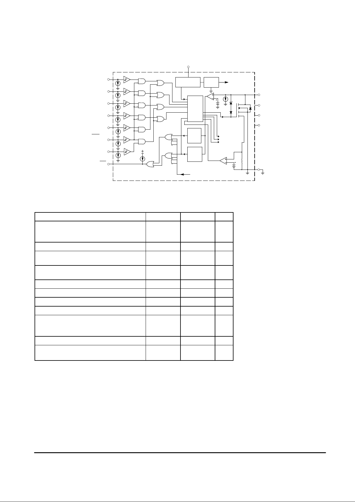
MAXIMUM RATINGS
Rating Symbol Value Unit
VCC V
Steady-State V
PWR
–13 to 30
Transient Conditions V
PWR(pk)
–13 to 60
Input Pin Voltage V
in
– 0.5 to 7.5 V
ESD Capability V
ESD
V
Human Body Model (R = 1.5 kΩ, C = 200 pf) 2000
Lead Current (per Output) I
Out
Internally A
Limited
Single Pulse Clamp Energy @ 25°C, 1.5 A E
clamp
100 mJ
Storage Temperature T
stg
– 55 to +150 °C
Operating Temperature T
J
– 40 to +150 °C
Lead Temperature (Wave Solder, 10 s) T
solder
260 °C
Power Dissipation @ TA = 105°C
P
D
11.25
W
Power Dissipation @ TA = 125°C
D
6.25
Derate for every °C above 25°C 0.25 W/°C
Thermal Resistance Junction-to-Ambient R
θJA
35 °C/W
Thermal Resistance Junction-to-Case.
Any one O/P
R
θJC
4.0 °C/W

MC33293A
3
MOTOROLA ANALOG IC DEVICE DATA
STATIC ELECTRICAL CHARACTERISTICS (9.0 V ≤ V
PWR
≤ 14.5 V and – 40°C ≤ TC ≤ +125°C, unless otherwise
noted. Typical values are at 25°C, unless otherwise noted.)
Characteristic
Symbol Min Typ Max Unit
INPUT
Turn ON Threshold V
on(th)
— 3.4 5.5 V
Operating Voltage Range V
PWR
5.5 — 30 V
Quiescent Power Supply Current (All Inputs off) I
PWR
— 2.2 5.0 mA
Overvoltage Shutdown Range V
PWR(ov)
30 35 38 V
Overvoltage Reset Hysteresis V
PWR(hys)
2.0 5.0 7.0 V
Input Voltage V
High (IDS = 1.0 A) V
IH
3.0 2.3 —
Low (IDS = 80 µA) V
IL
— 1.6 0.8
Input High Hysteresis (IDS = 1.0 A) V
IH(hys)
0.4 0.7 — V
Input Current µA
High (VIH = 3.0 V) I
IH
— 11 50
Low (VIL = 0.8 V) I
IL
— 11 50
OUTPUT
Static Drain-Source On-Resistance RDS
(on)
Ω
(IDS = 1.0 A, V
PWR
= 13 V, TC =–40°C to + 25°C) — 0.18 0.25
(IDS = 1.0 A, V
PWR
= 13 V, TC = +125°C) — 0.28 0.50
(IDS = 0.7 A, V
PWR
= 8.0 V, TC =+25°C) — 0.20 0.40
(IDS = 0.4 A, V
PWR
= 5.5 V, TC =+25°C) — 0.22 0.50
Drain-Source Clamp Voltage BV
DSS
V
(IDS = 20 mA, Vin =0 V, t
clamp
= 100 µs) 55 64 80
Zero Input Voltage Drain Current I
DS(off)
(VDS = 25 V, V
PWR
= 14.5 V) 10 23 80 µA
(VDS = 58 V, V
PWR
= 14.5 V) — 0.06 2.0 mA
Source Drain Diode Forward Voltage (ISD = 1.0 A) V
SD
— 0.62 1.4 V
MC33293A
4
MOTOROLA ANALOG IC DEVICE DATA
STATIC ELECTRICAL CHARACTERISTICS (continued)
(9.0 V ≤ V
PWR
≤ 14.5 V and – 40°C ≤ TC ≤ +125°C, unless otherwise
noted. Typical values are at 25°C, unless otherwise noted.)
Characteristic UnitMaxTypMinSymbol
FAULT STATUS OUTPUTT
Fault Status Pin V
Low Voltage (V
PWR
= 14.5 V, I
stl
= 1.0 mA, open-load on
Output 1, 2, 3 or 4. All inputs = 0 V)
V
stl
— 0.1 0.4
High Voltage, (V
PWR
= 14.5 V, I
sth
= – 30 µA, Note 1) V
sth
3.0 4.7 5.5
FAULT DETECTION
Output Limiting Current (V
PWR
= 13 V) I
DS(limit)
3.0 4.0 6.0 A
Over-Current Detect Voltage Threshold and V
OC(limit)
2.4 3.7 5.0 V
Output-Off Open-Load Detect Threshold V oltage V
Ooff(th)
2.4 3.7 5.0
output-on open-load Detect Current I
Oon(th)
mA
(V
PWR
= 13 V, Vin = 5.0 V, TC =–40°C) 20 80 190
(V
PWR
= 13 V, Vin = 5.0 V, TC =+25°C) 20 75 130
(V
PWR
= 13 V, Vin = 5.0 V, TC = +125°C) 20 65 100
DYNAMIC ELECTRIC CHARACTERISTICS
Characteristic Symbol Min Typ Max Unit
OUTPUT TIMING
Output Driver Rise Time (VCC = 13 V, RL = 13 Ω , t
r
—
µs
tr = Output Voltage change from 90% to 10%, see Figure 2)
—
2.3
10
Output Driver Fall Time (VCC = 13 V, RL = 13 Ω , t
f
—
µs
tf = Output Voltage change from 10% to 90%, see Figure 2)
—
1.5
10
Output Delay Time (VCC = 13 V, RL = 13 Ω , µs
t
on(dly)
= Vin at 3.0 V to VO at 90%, see Figure 2) t
on(dly)
— 3.2 10
t
off(dly)
= Vin at 1.0 V to VO at 10%, see Figure 2) t
off(dly)
— 5.9 15
FAULT TIMING
Over-Current Sense Time (See Figure 5 or 6) t
oc
µs
(Vin = 5.0 V, RL = 0.05 Ω , V
PWR
= 14.5 V , 10 55 250
over-current duty cycle ≤ 10%
toc = time that V
Status
is > 1.0 V)
Over-Current Refresh Time (See Figures 5 or 6) t
ref
ms
(Vin = 5.0 V, RL = 0.05 Ω , V
PWR
= 14.5 V , 1.5 3.6 7.0
over-current duty cycle ≤ 10%
t
ref
= time that V
Status
is < 1.0 V)
Output Open-Load Fault Status Delay Time ms
(V
PWR
= 13 V, Vin = 5.0 V, open-load on Output, t
os(on)
t
os(on)
= time from Vin = 3.0 V to V
Status
= 1.0 V, see Figure 3) 1.0 2.2 4.0
(V
PWR
= 13 V, Vin = 0 V , open-load on Output, t
os(off)
µs
t
os(off)
= time from Vin = 2.5 V to V
Status
= 1.0 V, see Figure 4) 1.0 19 40
Fault Status Reset Delay Time t
s(reset)
µs
(V
PWR
= 13 V, Vin = 0 V, see Figure 4) — 2.0 10
NOTE: 1. Negative current signifies current flowing out of device.
t
MC33293A
5
MOTOROLA ANALOG IC DEVICE DATA
G4
I
Limit
23
µ
A
G3
I
Limit
G2
I
Limit
R
S
I
Limit
Injector 4
(14
Ω
, 10mH)
(1)
Injector 3
(14
Ω
, 10mH)
(1)
Injector 2
(14Ω, 10mH)
(1)
Injector 1
(14
Ω
, 10mH)
(1)
8
15
14
1
2
G4
G3
G2
Bias
Short
Circuit
Detect
Open
Load
Detect
Short
Circuit
Detect
Open
Load
Detect
Short
Circuit
Detect
Open
Load
Detect
Short
Circuit
Detect
Open
Load
Detect
Gate
Control
Bias
Circuit
Overvoltage
Shutdown
7
11
µ
A x 7
100
µ
A
Fault
Encoder
10
11
6
5
12
13
4
3
Input 3 & 4
Select
Input 1 & 2
Input 4
Input 3
Input 2
Input 1
IRQ
Fault
PD 2
PD 1
PD 0
OC 5
OC 4
OC 3
OC 2
MC68HC11A1
+14V
V
Load
(Battery)
23µA
23
µ
A
23
µ
A
NOTE: 1. The MC33293A
is also designed to drive
the 194 type incandescent
instrument lamp.
Figure 1. Fuel Injector Application Block Diagram
R
S
R
S
R
S
 Loading...