

8
1
P SUFFIX
PLASTIC PACKAGE
CASE 626
Device
Operating
Temperature Range
Package
SEMICONDUCTOR
TECHNICAL DATA
ISO SERIAL LINK
INTERFACE
ORDERING INFORMATION
MC33290D
MC33290P
TA = –40° to +125°C
SO–8
DIP–8
PIN CONNECTIONS
Order this document by MC33290/D
18
7
6
5
2
3
4
V
BB
N/C
Gnd
Tx
(Top View)
ISO
(K Line I/O)
Rx
V
DD
CEN
D SUFFIX
PLASTIC PACKAGE
CASE 751
(SO–8)
8
1
1
MOTOROLA ANALOG IC DEVICE DATA
The MC33290 is a serial link bus interface device designed to provide
bi–directional half–duplex communication interfacing in automotive
diagnostic applications. It is designed to interface between the vehicle’s
on–board microcontroller and systems off–board the vehicle via the special
ISO K line. The MC33290 is designed to meet the “Diagnostic Systems
ISO9141” specification. The device’s K line bus driver’s output is fully
protected against bus shorts and over temperature conditions.
The MC33290 derives it’s robustness to temperature and voltage
extremes from being built on a SMARTMOS
process, incorporating CMOS
logic, bipolar/MOS analog circuitry, and DMOS power FETs. Though the
MC33290 was principally designed for automotive applications, it is suited for
other serial communication applications. It is parametrically specified over an
ambient temperature range of –40°C ≤ TA ≤ 125°C and 8.0 V ≤ V
Bat
≤ 18 V
supply. The economical 8 pin DIP and SO–8 surface mount plastic packages
make the MC33290 very cost effective.
• Designed to Operate Over Wide Supply Voltage of 8.0 to 18 V
• Ambient Operating Temperature of –40°C to 125°C
• Interfaces Directly to Standard CMOS Microprocessors
• ISO K Line Pin Protected Against Shorts to Ground
• Thermal Shutdown with Hysteresis
• Maximum Transmission Speeds in Excess of 50 k Baud
• ISO K Line Pin Capable of High Currents
• ISO K Line can be Driven with up to 10 nF of Parasitic Capacitance
• 8.0 kV ESD Protection Attainable with Few Additional Components
• Standby Mode: No V
Bat
Current Drain with VDD at 5.0 V
• Low Current Drain during Operation with V
DD
at 5.0 V
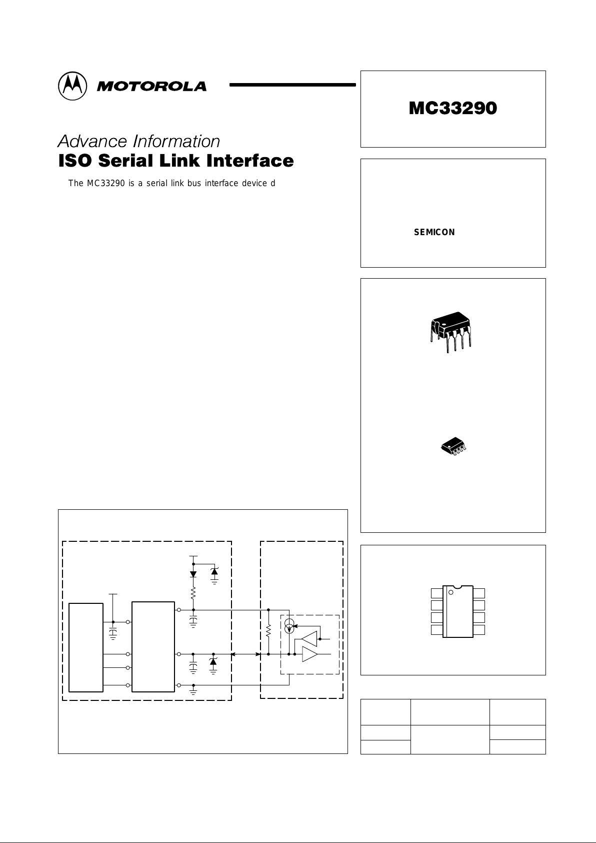
Typical Application Schematic
This device contains 85 active transistors.
Components Necessary for: Reverse Battery (1), Overvoltage Transient (2), and
8.0 kV ESD Protection (3) in a metal module case.
V
CC
D
x
SCIRxD
SCITxD
MCU
V
DD
CEN
Rx
Tx
V
BB
ISO
Gnd
5.0 nF(3)
27 V(3)
1.0 nF
5.0 V
10 nF(3)
500
Ω
(2)
D(1)
45 V(2)
+V
Bat
+V
DD
ISO
K Line
510
Ω
Service Scan Tool
or
End of Production Line
Programming
or
System Checking
On–Board Diagnostic Link
MC33290
TxD
RxD
6
5
7
8
3
4
1
This document contains information on a new product. Specifications and information herein
are subject to change without notice.
Motorola, Inc. 1997 Rev 0
MC33290
2
MOTOROLA ANALOG IC DEVICE DATA
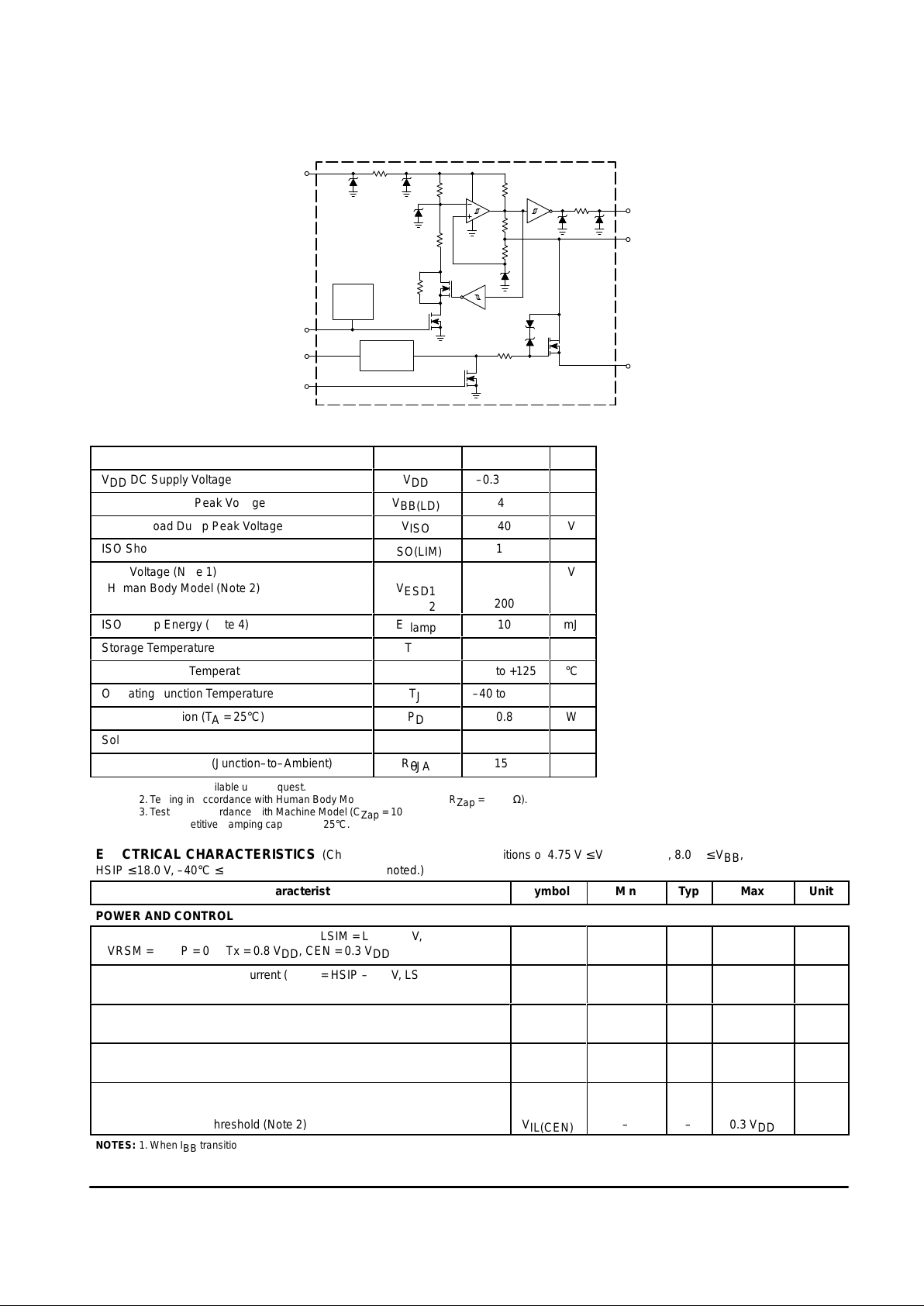
Figure 1. Simplified Block Diagram
V
BB
CEN
V
DD
Tx
Rx
ISO
Gnd
40 V
Thermal
Shutdown
R
Hys
Master
Bias
6
4
3
1
8
7
5
MAXIMUM RATINGS (All voltages are with respect to ground, unless otherwise noted.)
Rating Symbol Value Unit
VDD DC Supply Voltage
V
DD
–0.3 to 7.0
V
VBB Load Dump Peak Voltage
V
BB(LD)
45
V
ISO Pin Load Dump Peak Voltage
V
ISO
40
V
ISO Short Circuit Current Limit
I
ISO(LIM)
1.0
A
ESD Voltage (Note 1)
V
Human Body Model (Note 2) V
ESD1
2000
Machine Model (Note 3) V
ESD2
200
ISO Clamp Energy (Note 4)
E
clamp
10
mJ
Storage Temperature
T
stg
–55 to +150
°C
Operating Case Temperature
T
C
–40 to +125
°C
Operating Junction Temperature
T
J
–40 to +150
°C
Power Dissipation (TA = 25°C)
P
D
0.8
W
Soldering Temperature (for 10 seconds)
T
solder
260
°C
Thermal Resistance (Junction–to–Ambient)
R
θJA
150
°C/W
NOTES: 1. ESD data available upon request.
2.Testing in accordance with Human Body Model (C
Zap
= 100 pF, R
Zap
= 1500 Ω).
3.Testing in accordance with Machine Model (C
Zap
= 100 pF, R
Zap
= 0Ω).
4.Non–repetitive clamping capability at 25°C.
ELECTRICAL CHARACTERISTICS (Characteristics noted under conditions of 4.75 V ≤ V
DD
≤ 5.25 V, 8.0 V ≤ VBB,
HSIP ≤ 18.0 V, –40°C ≤ TC ≤ 125°C, unless otherwise noted.)
Characteristic
Symbol Min Typ Max Unit
POWER AND CONTROL
ББББББББББББББББББ
Á
VDD Sleep State Current (HSIM = HSIP, LSIM = LSIP = 0 V,
VRSM = VRSP = 0 V, Tx = 0.8 VDD, CEN = 0.3 VDD)
ÁÁÁÁ
ÁÁÁ
Á
I
DD(SS)
ÁÁ
Á
–
Á
Á
–
ÁÁÁ
Á
0.1
Á
Á
mA
ББББББББББББББББББ
VDD Quiescent Operating Current (HSIM = HSIP – 0.3 V, LSIM = 0 V,
LSIP = 0.3 V, VRSM = 0 V, VRSP = –0.5 V, Tx = 0.2 VDD, CEN = 0.7 VDD)
ÁÁÁÁ
ÁÁÁ
I
DD(Q)
ÁÁ–Á–ÁÁÁ
1.0
Á
mA
ББББББББББББББББББ
Á
VBB Sleep State Current (VBB = 16 V, HSIM = HSIP, LSIM = LSIP = 0 V,
VRSM = VRSP = 0 V, Tx = 0.8 VDD, CEN = 0.3 VDD)
ÁÁÁÁ
ÁÁÁ
Á
I
BB(SS)
ÁÁ
Á
–
Á
Á
–
ÁÁÁ
Á
50
Á
Á
µA
ББББББББББББББББББ
Á
VBB Quiescent Operating Current (HSIM = HSIP – 0.3 V, LSIM = 0 V,
LSIP = 0.3 V, VRSM = 0 V, VRSP = –0.5 V, Tx = 0.2 VDD, CEN = 0.7 VDD)
ÁÁÁÁ
ÁÁÁ
Á
I
BB(Q)
ÁÁ
Á
–
Á
Á
–
ÁÁÁ
Á
1.0
Á
Á
mA
Chip Enable
ÁÁÁÁ
V
Input High Voltage Threshold (Note 1) V
IH(CEN)
0.7 V
DD
– –
Input Low Voltage Threshold (Note 2) V
IL(CEN)
– – 0.3 V
DD
NOTES: 1. When IBB transitions to >100 µA.
2.When IBB transitions to <100 µA.
 Loading...