

Motorola MC33264D-5.0, MC33264DM-2.8, MC33264DM-4.75, MC33264DM-3.8, MC33264DM-4.0 Datasheet
...
Order this document by MC33264/D
The MC33264 series are micropower low dropout voltage regulators
available in SO–8 and Micro–8 surface mount packages and a wide range of
output voltages. These devices feature a very low quiescent current (100 µA
in the ON mode; 0.1 µA in the OFF mode), and are capable of supplying
output currents up to 100 mA. Internal current and thermal limiting protection
is provided. They require only a small output capacitance for stability .
Additionally, the MC33264 has either active HIGH or active LOW control
(Pins 2 and 3) that allows a logic level signal to turn–off or turn–on the
regulator output.
Due to the low input–to–output voltage differential and bias current
specifications, these devices are ideally suited for battery powered
computer, consumer, and industrial equipment where an extension of useful
battery life is desirable.
MC33264 Features:
• Low Quiescent Current (0.3 µA in OFF Mode; 95 µA in ON Mode)
• Low Input–to–Output Voltage Dif ferential of 47 mV at 10 mA, and
131 mV at 50 mA
• Multiple Output Voltages A vailable
• Extremely Tight Line and Load Regulation
• Stable with Output Capacitance of Only
0.22 µF for 4.0 V, 4.75 V and 5.0 V Output V oltages
0.33 µF for 2.8 V, 3.0 V, 3.3 V and 3.8 V Output Voltages
• Internal Current and Thermal Limiting
• Logic Level ON/OFF Control
• Functionally Equivalent to TK1 15XXMC and LP2980
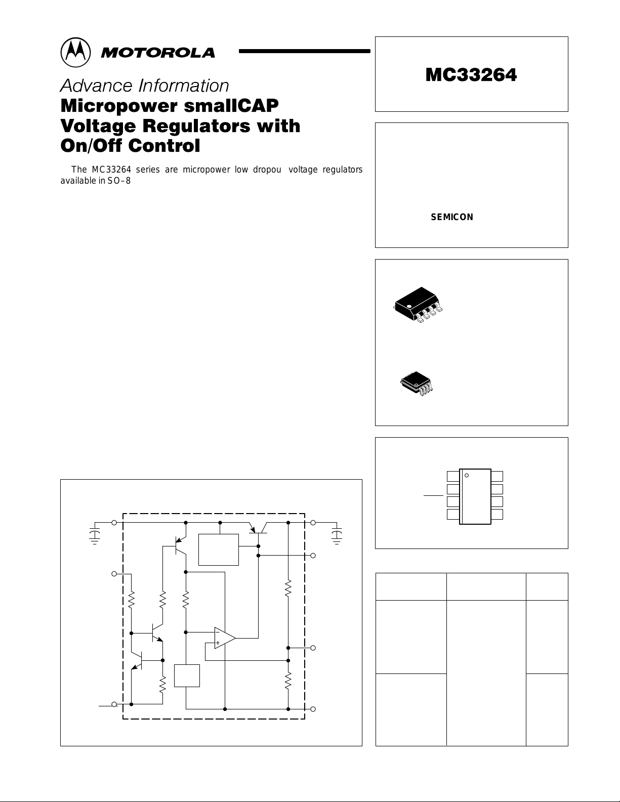
Representative Block Diagram
1
V
in
2
On/Off
3
On/Off
This device contains 37 active transistors.
This document contains information on a new product. Specifications and information herein
are subject to change without notice.
MOTOROLA ANALOG IC DEVICE DATA
1.23 V
V
ref
MC33264
Thermal and
Anti–Sat
Protection
R
int
52.5 k
8
V
out
7
Base
5
Adj
6
Gnd
LOW DROPOUT
MICROPOWER VOLTAGE
REGULATORS WITH
ON/OFF CONTROL
SEMICONDUCTOR
TECHNICAL DATA
D SUFFIX
PLASTIC PACKAGE
8
1
8
1
PIN CONNECTIONS
1
Input
2
On/Off
3
On/Off
4
N/C
(Top View)
ORDERING INFORMATION
Device
MC33264D–2.8
MC33264D–3.0
MC33264D–3.3
MC33264D–3.8
MC33264D–4.0
MC33264D–4.75
MC33264D–5.0
MC33264DM–2.8
MC33264DM–3.0
MC33264DM–3.3
MC33264DM–3.8
MC33264DM–4.0
MC33264DM–4.75
MC33264DM–5.0
Motorola, Inc. 1997 Rev 1
Temperature Range
TA = – 40° to +85°C
CASE 751
(SO–8)
DM SUFFIX
PLASTIC PACKAGE
CASE 846A
(Micro–8)
8
Output
7
Base
6
Gnd
5
Adjust
Operating
Package
SO–8
Micro–8
1
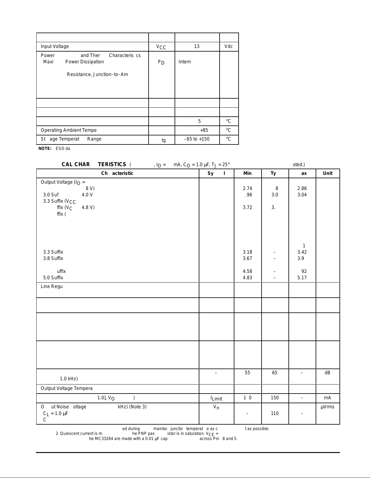
MAXIMUM RATINGS
ÁÁÁ
ÁÁÁ
ÁÁÁ
ÁÁÁ
ÁÁÁ
Á
Á
Á
Á
Á
ÁÁÁ
Á
ÁÁÁ
ÁÁÁ
ÁÁÁ
(TC = 25°C, unless otherwise noted.)
Rating
Input Voltage
Power Dissipation and Thermal Characteristics
Maximum Power Dissipation P
Case 751 (SO–8) D Suffix
Thermal Resistance, Junction–to–Ambient R
Thermal Resistance, Junction–to–Case R
Case 846A (Micro–8) DM Suffix
Thermal Resistance, Junction–to–Ambient R
Output Current
Maximum Adjustable Output Voltage
Operating Junction Temperature
Operating Ambient Temperature
Storage Temperature Range
NOTE: ESD data available upon request.
MC33264
Symbol Value Unit
V
T
CC
θJA
θJC
θJA
I
O
V
T
T
stg
D
O
J
A
13
Vdc
Internally Limited W
180 °C/W
45 °C/W
240 °C/W
100
1.15 x V
nom
125
–40 to +85
–65 to +150
mA
Vdc
°C
°C
°C
ELECTRICAL CHARACTERISTICS (V
= 6.0 V, IO = 10 mA, CO = 1.0 µF, TJ = 25°C (Note 1), unless otherwise noted.)
in
Characteristic Symbol Min Typ Max Unit
Output Voltage (IO = 0 mA)
V
O
2.8 Suffix (VCC = 3.8 V) 2.74 2.8 2.86
3.0 Suffix (VCC = 4.0 V) 2.96 3.0 3.04
3.3 Suffix (VCC = 4.3 V) 3.23 3.3 3.37
3.8 Suffix (VCC = 4.8 V) 3.72 3.8 3.88
4.0 Suffix (VCC = 5.0 V) 3.92 4.0 4.08
4.75 Suffix (VCC = 5.75 V) 4.66 4.75 4.85
5.0 Suffix (VCC = 6.0 V) 4.9 5.0 5.1
Vin = (VO + 1.0) V to 12 V, IO < 60 mA,TA= –40° to +85°C
2.8 Suffix 2.7 – 2.9
3.0 Suffix 2.9 – 3.1
3.3 Suffix 3.18 – 3.42
3.8 Suffix 3.67 – 3.93
4.0 Suffix 3.86 – 4.14
4.75 Suffix 4.58 – 4.92
5.0 Suffix 4.83 – 5.17
Line Regulation (Vin = [VO + 1.0] V to 12 V, IO = 60 mA)
Reg
line
–
2.0
All Suffixes
Load Regulation (Vin = [VO + 1.0], IO = 0 mA to 60 mA)
Reg
load
–
16
All Suffixes
Dropout Voltage
VI – V
O
IO = 10 mA – 47 90
IO = 50 mA – 131 200
IO = 60 mA – 147 230
Quiescent Current
I
Q
ON Mode (Vin = [VO + 1.0] V, IO = 0 mA) – 95 150
OFF Mode – 0.3 2.0
ON Mode (Vin = [VO + 0.5] V, IO = 0 mA) [Note2] – 540 900
Ripple Rejection (Vin peak–to–peak = [VO + 1.5] to [VO + 5.5]
БББББББББББББББББ
V at f = 1.0 kHz)
Output Voltage Temperature Coefficient
Current Limit (Vin = [VO + 1.0], VO Shorted)
Output Noise Voltage (10 Hz to 100 kHz) (Note 3)
–
ÁÁÁ
TC
I
Limit
V
n
55
ÁÁ
–
100
65
ÁÁ
±120
150
CL = 1.0 µF – 110 –
CL = 100 µF – 46 –
NOTES: 1. Low duty pulse techniques are used during test to maintain junction temperature as close to ambient as possible.
2.Quiescent current is measured where the PNP pass transistor is in saturation. VCE = –0.5 V guarantees this condition.
3.Noise tests on the MC33264 are made with a 0.01 µF capacitor connected across Pins 8 and 5.
10
25
–
ÁÁ
–
–
V
mV
mV
mV
µA
dB
ÁÁ
ppm/°C
mA
µVrms
2
MOTOROLA ANALOG IC DEVICE DATA
MC33264
ÁÁÁ
ÁÁÁ
ELECTRICAL CHARACTERISTICS (continued) (V
Characteristic UnitMaxTypMinSymbol
ON/OFF INPUTS
On/Off Input (Pin 3 Tied to Ground)
Logic “1” (Regulator ON) 2.4 – V
Logic “0” (Regulator OFF) 0 – 0.5
On/Off Input (Pin 2 Tied to Vin)
Logic “0” (Regulator ON) 0 – Vin – 2.4
Logic “1” (Regulator OFF) Vin – 0.2 – V
On/Off Pin Input Current (Pin 3 Tied to Ground)
V
= 2.4 V – 1.9 –
On/Off
On/Off Pin Input Current (Pin 2 Tied to Vin)
V
= Vin – 2.4 V – 12 –
On/Off
NOTES: 1. Low duty pulse techniques are used during test to maintain junction temperature as close to ambient as possible.
2.Quiescent current is measured where the PNP pass transistor is in saturation. VCE = –0.5 V guarantees this condition.
3.Noise tests on the MC33264 are made with a 0.01 µF capacitor connected across Pins 8 and 5.
= 6.0 V, IO = 10 mA, CO = 1.0 µF, TJ = 25°C (Note 1), unless otherwise noted.)
in
V
On/Off
I
On/Off
DEFINITIONS
Dropout V oltage – The input/output voltage dif ferential at
which the regulator output no longer maintains regulation
against further reductions in input voltage. Measured when
the output drops 100 mV below its nominal value (which is
measured at 1.0 V differential), dropout voltage is affected by
junction temperature, load current and minimum input supply
requirements.
Line Regulation – The change in output voltage for a
change in input voltage. The measurement is made under
conditions of low dissipation or by using pulse techniques such
that average chip temperature is not significantly affected.
Load Regulation – The change in output voltage for a
change in load current at constant chip temperature.
Maximum Power Dissipation – The maximum total
device dissipation for which the regulator will operate within
specifications.
Quiescent Current – Current which is used to operate the
regulator chip and is not delivered to the load.
Output Noise V oltage – The rms ac voltage at the output,
with constant load and no input ripple, measured over a
specified frequency range.
V
in
in
µA
5.0
1.0
, QUIESCENT CURRENT (mA)
Q
0.10
I
0.03
TA = 25°C
MC33264D–5.0
0.1
Figure 1. Quiescent Current
versus Load Current
1.0 10 100 1.0 2.0 3.0 4.0 5.0 6.0
I
, LOAD CURRENT (mA)
load
Figure 2. Output V oltage versus Input Voltage
6.0
TA = 25°C
5.0
MC33264D–5.0
, OUTPUT VOL TAGE (V)
V
4.0
3.0
2.0
O
1.0
0
0
RL = 5.0 k
RL = 100
Vin, INPUT VOLTAGE (V)
Ω
MOTOROLA ANALOG IC DEVICE DATA
3
 Loading...