

查询MC33264D-3.0供应商
Order this document by MC33264/D
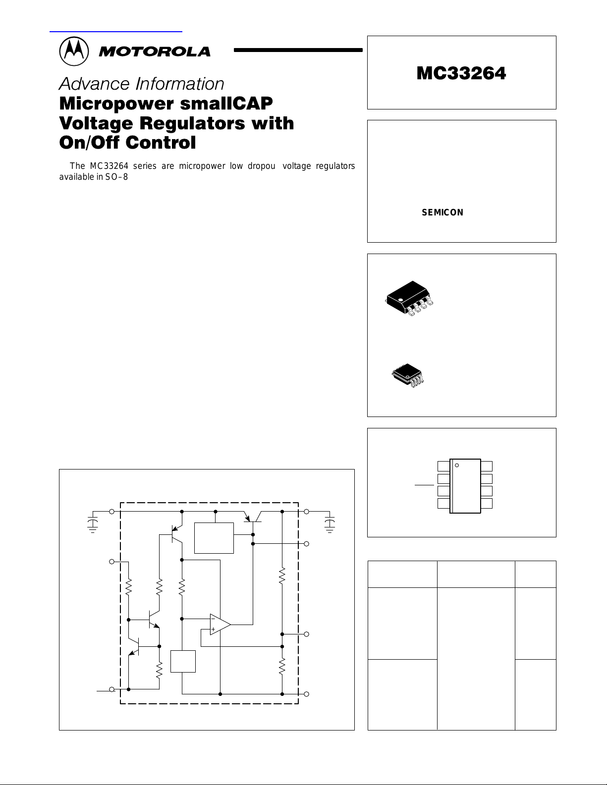
The MC33264 series are micropower low dropout voltage regulators
available in SO–8 and Micro–8 surface mount packages and a wide range of
output voltages. These devices feature a very low quiescent current (100 µA
in the ON mode; 0.1 µA in the OFF mode), and are capable of supplying
output currents up to 100 mA. Internal current and thermal limiting protection
is provided. They require only a small output capacitance for stability .
Additionally, the MC33264 has either active HIGH or active LOW control
(Pins 2 and 3) that allows a logic level signal to turn–off or turn–on the
regulator output.
Due to the low input–to–output voltage differential and bias current
specifications, these devices are ideally suited for battery powered
computer, consumer, and industrial equipment where an extension of useful
battery life is desirable.
MC33264 Features:
• Low Quiescent Current (0.3 µA in OFF Mode; 95 µA in ON Mode)
• Low Input–to–Output Voltage Dif ferential of 47 mV at 10 mA, and
131 mV at 50 mA
• Multiple Output Voltages A vailable
• Extremely Tight Line and Load Regulation
• Stable with Output Capacitance of Only
0.22 µF for 4.0 V, 4.75 V and 5.0 V Output V oltages
0.33 µF for 2.8 V, 3.0 V, 3.3 V and 3.8 V Output Voltages
• Internal Current and Thermal Limiting
• Logic Level ON/OFF Control
• Functionally Equivalent to TK1 15XXMC and LP2980
Representative Block Diagram
1
V
in
2
On/Off
3
On/Off
This device contains 37 active transistors.
This document contains information on a new product. Specifications and information herein
are subject to change without notice.
MOTOROLA ANALOG IC DEVICE DATA
1.23 V
V
ref
MC33264
Thermal and
Anti–Sat
Protection
R
int
52.5 k
8
V
out
7
Base
5
Adj
6
Gnd
LOW DROPOUT
MICROPOWER VOLTAGE
REGULATORS WITH
ON/OFF CONTROL
SEMICONDUCTOR
TECHNICAL DATA
D SUFFIX
PLASTIC PACKAGE
8
1
8
1
PIN CONNECTIONS
1
Input
2
On/Off
3
On/Off
4
N/C
(Top View)
ORDERING INFORMATION
Device
MC33264D–2.8
MC33264D–3.0
MC33264D–3.3
MC33264D–3.8
MC33264D–4.0
MC33264D–4.75
MC33264D–5.0
MC33264DM–2.8
MC33264DM–3.0
MC33264DM–3.3
MC33264DM–3.8
MC33264DM–4.0
MC33264DM–4.75
MC33264DM–5.0
Motorola, Inc. 1997 Rev 1
Temperature Range
TA = – 40° to +85°C
CASE 751
(SO–8)
DM SUFFIX
PLASTIC PACKAGE
CASE 846A
(Micro–8)
8
Output
7
Base
6
Gnd
5
Adjust
Operating
Package
SO–8
Micro–8
1
MAXIMUM RATINGS
ÁÁÁ
ÁÁÁ
ÁÁÁ
ÁÁÁ
ÁÁÁ
Á
Á
Á
Á
Á
ÁÁÁ
Á
ÁÁÁ
ÁÁÁ
ÁÁÁ
(TC = 25°C, unless otherwise noted.)
Rating
Input Voltage
Power Dissipation and Thermal Characteristics
Maximum Power Dissipation P
Case 751 (SO–8) D Suffix
Thermal Resistance, Junction–to–Ambient R
Thermal Resistance, Junction–to–Case R
Case 846A (Micro–8) DM Suffix
Thermal Resistance, Junction–to–Ambient R
Output Current
Maximum Adjustable Output Voltage
Operating Junction Temperature
Operating Ambient Temperature
Storage Temperature Range
NOTE: ESD data available upon request.
MC33264
Symbol Value Unit
V
T
CC
θJA
θJC
θJA
I
O
V
T
T
stg
D
O
J
A
13
Vdc
Internally Limited W
180 °C/W
45 °C/W
240 °C/W
100
1.15 x V
nom
125
–40 to +85
–65 to +150
mA
Vdc
°C
°C
°C
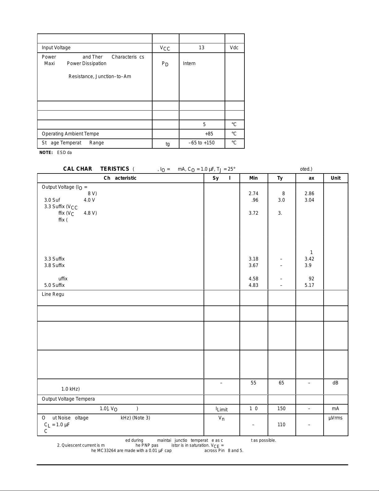
ELECTRICAL CHARACTERISTICS (V
= 6.0 V, IO = 10 mA, CO = 1.0 µF, TJ = 25°C (Note 1), unless otherwise noted.)
in
Characteristic Symbol Min Typ Max Unit
Output Voltage (IO = 0 mA)
V
O
2.8 Suffix (VCC = 3.8 V) 2.74 2.8 2.86
3.0 Suffix (VCC = 4.0 V) 2.96 3.0 3.04
3.3 Suffix (VCC = 4.3 V) 3.23 3.3 3.37
3.8 Suffix (VCC = 4.8 V) 3.72 3.8 3.88
4.0 Suffix (VCC = 5.0 V) 3.92 4.0 4.08
4.75 Suffix (VCC = 5.75 V) 4.66 4.75 4.85
5.0 Suffix (VCC = 6.0 V) 4.9 5.0 5.1
Vin = (VO + 1.0) V to 12 V, IO < 60 mA,TA= –40° to +85°C
2.8 Suffix 2.7 – 2.9
3.0 Suffix 2.9 – 3.1
3.3 Suffix 3.18 – 3.42
3.8 Suffix 3.67 – 3.93
4.0 Suffix 3.86 – 4.14
4.75 Suffix 4.58 – 4.92
5.0 Suffix 4.83 – 5.17
Line Regulation (Vin = [VO + 1.0] V to 12 V, IO = 60 mA)
Reg
line
–
2.0
All Suffixes
Load Regulation (Vin = [VO + 1.0], IO = 0 mA to 60 mA)
Reg
load
–
16
All Suffixes
Dropout Voltage
VI – V
O
IO = 10 mA – 47 90
IO = 50 mA – 131 200
IO = 60 mA – 147 230
Quiescent Current
I
Q
ON Mode (Vin = [VO + 1.0] V, IO = 0 mA) – 95 150
OFF Mode – 0.3 2.0
ON Mode (Vin = [VO + 0.5] V, IO = 0 mA) [Note2] – 540 900
Ripple Rejection (Vin peak–to–peak = [VO + 1.5] to [VO + 5.5]
БББББББББББББББББ
V at f = 1.0 kHz)
Output Voltage Temperature Coefficient
Current Limit (Vin = [VO + 1.0], VO Shorted)
Output Noise Voltage (10 Hz to 100 kHz) (Note 3)
–
ÁÁÁ
TC
I
Limit
V
n
55
ÁÁ
–
100
65
ÁÁ
±120
150
CL = 1.0 µF – 110 –
CL = 100 µF – 46 –
NOTES: 1. Low duty pulse techniques are used during test to maintain junction temperature as close to ambient as possible.
2.Quiescent current is measured where the PNP pass transistor is in saturation. VCE = –0.5 V guarantees this condition.
3.Noise tests on the MC33264 are made with a 0.01 µF capacitor connected across Pins 8 and 5.
10
25
–
ÁÁ
–
–
V
mV
mV
mV
µA
dB
ÁÁ
ppm/°C
mA
µVrms
2
MOTOROLA ANALOG IC DEVICE DATA
MC33264
ÁÁÁ
ÁÁÁ
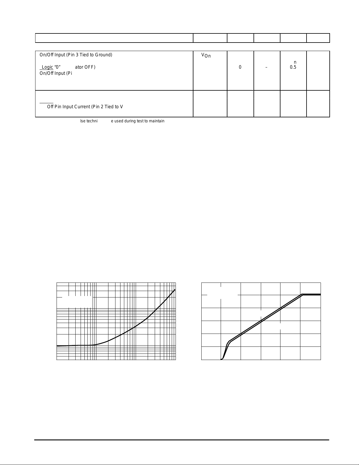
ELECTRICAL CHARACTERISTICS (continued) (V
Characteristic UnitMaxTypMinSymbol
ON/OFF INPUTS
On/Off Input (Pin 3 Tied to Ground)
Logic “1” (Regulator ON) 2.4 – V
Logic “0” (Regulator OFF) 0 – 0.5
On/Off Input (Pin 2 Tied to Vin)
Logic “0” (Regulator ON) 0 – Vin – 2.4
Logic “1” (Regulator OFF) Vin – 0.2 – V
On/Off Pin Input Current (Pin 3 Tied to Ground)
V
= 2.4 V – 1.9 –
On/Off
On/Off Pin Input Current (Pin 2 Tied to Vin)
V
= Vin – 2.4 V – 12 –
On/Off
NOTES: 1. Low duty pulse techniques are used during test to maintain junction temperature as close to ambient as possible.
2.Quiescent current is measured where the PNP pass transistor is in saturation. VCE = –0.5 V guarantees this condition.
3.Noise tests on the MC33264 are made with a 0.01 µF capacitor connected across Pins 8 and 5.
= 6.0 V, IO = 10 mA, CO = 1.0 µF, TJ = 25°C (Note 1), unless otherwise noted.)
in
V
On/Off
I
On/Off
DEFINITIONS
Dropout V oltage – The input/output voltage dif ferential at
which the regulator output no longer maintains regulation
against further reductions in input voltage. Measured when
the output drops 100 mV below its nominal value (which is
measured at 1.0 V differential), dropout voltage is affected by
junction temperature, load current and minimum input supply
requirements.
Line Regulation – The change in output voltage for a
change in input voltage. The measurement is made under
conditions of low dissipation or by using pulse techniques such
that average chip temperature is not significantly affected.
Load Regulation – The change in output voltage for a
change in load current at constant chip temperature.
Maximum Power Dissipation – The maximum total
device dissipation for which the regulator will operate within
specifications.
Quiescent Current – Current which is used to operate the
regulator chip and is not delivered to the load.
Output Noise V oltage – The rms ac voltage at the output,
with constant load and no input ripple, measured over a
specified frequency range.
V
in
in
µA
5.0
1.0
, QUIESCENT CURRENT (mA)
Q
0.10
I
0.03
TA = 25°C
MC33264D–5.0
0.1
Figure 1. Quiescent Current
versus Load Current
1.0 10 100 1.0 2.0 3.0 4.0 5.0 6.0
I
, LOAD CURRENT (mA)
load
Figure 2. Output V oltage versus Input Voltage
6.0
TA = 25°C
5.0
MC33264D–5.0
, OUTPUT VOL TAGE (V)
V
4.0
3.0
2.0
O
1.0
0
0
RL = 5.0 k
RL = 100
Vin, INPUT VOLTAGE (V)
Ω
MOTOROLA ANALOG IC DEVICE DATA
3

MC33264
Figure 3. Input Current versus Input Voltage Figure 4. Output Voltage versus Temperature
, OUTPUT VOL TAGE (V)
V
O
5.04
5.03
5.02
5.01
5.00
4.99
4.98
4.97
4.96
–55
IO = 10 mA
TA = 25
MC33264D–5.0
–25 25
TA, AMBIENT TEMPERATURE (
°
C
1000
A)
µ
, INPUT CURRENT (
in
I
800
600
400
200
No Load
°
C
TA = 25
MC33264D–5.0
0
0
2.0 4.0 8.0 10 12 0 50 75 100
Vin, INPUT VOLTAGE (V)
6.0
125
°
C)
Figure 5. Dropout Voltage versus Output Current Figure 6. Dropout Voltage versus Temperature
240
200
160
120
80
, DROPOUT VOLTAGE (mV)
O
– V
40
I
V
0
0.3
RL = 40 to 50 k
µ
CL = 1.0
TA = 25
MC33264D–5.0
1.0 10 400 0 50 100 150
F
°
C
IO, OUTPUT CURRENT (mA)
100
Ω
300
RL = 5.0 k
TA = 25
= 100 to 500
MC33264D–5.0
250
L
R
200
150
100
, DROPOUT VOLTAGE (mV)
O
50
– V
I
–50
V
°
C
TA, TEMPERATURE (°C)
RL = 100
RL = 5.0 k
RL = 500
APPLICATION INFORMATION
Introduction
The MC33264 regulators are designed with internal
current limiting and thermal shutdown making them
user–friendly. These regulators require only 0.33 µF (or
greater) capacitance between the output terminal and ground
for stability for 2.8 V, 3.0 V, 3.3 V and 3.8 V output voltage
options. Output voltage options of 4.0 V, 4.75 V and 5.0 V
require only 0.22 µF for stability. The output capacitor must
be mounted as close to the MC33264 as possible. If the
output capacitor must be mounted further than two
centimeters away from the MC33264, then a larger value of
output capacitor may be required for stability . A value of 0.68
µF or larger is recommended. Most types of aluminum,
tantalum or multilayer ceramic will perform adequately. Solid
tantalums or appropriate multilayer ceramic capacitors are
recommended for operation below 25°C.
A bypass capacitor is recommended across the MC33264
input to ground if more than 4.0 inches of wire connects the
input to either a battery or power supply filter capacitor.
On/Off Control
On/Off control of the regulator may be accomplished in
either of two ways. Pin 3 may be tied to circuit ground and a
positive logic control applied to Pin 2. The regulator will be
turned on by a positive (>2.4 V) level, typically 5.0 V with
respect to ground, sourcing a typical current of 6.0 µA. The
regulator will turn off if the control input is a logic “0”
(<0.5 V). Alternatively, Pin 2 may be tied to the regulator
input voltage and a negative logic control applied to Pin 3.
The regulator will be turned on when the control voltage is
less than Vin – 2.4 V , sinking a typical current of 18 µA when
Vin = 6.0 V. The regulator is off when the control input is
open or greater than Vin – 0.2 V.
Programming The Output Voltage
The MC33264 output voltage is automatically set using its
internal voltage divider. Alternatively, it may be programmed
within a typical ±15% range of its preset output voltage. An
external pair of resistors is required, as shown in Figure 7.
55
50
45
40
35
30
= 5.0 k
L
R
, DROPOUT VOLTAGE (mV)
O
– V
I
V
4
MOTOROLA ANALOG IC DEVICE DATA

3.3 µF
Control Input
2
MC33264
Figure 7. Regulator Output Voltage Trim
V
in
1
V
in
On/Off
V
out
Base
8
7
N/C
3.3
µ
F
V
out
3.0, 3.3 or 5.0 V
3
On/Off
Gnd Adj
65
The complete equation for the output voltage is:
R1
where V
ǒ
V
+
out
is the nominal 1.235 V reference voltage and IFB is
ref
1
V
ref
)
R2
Ǔ
)
IFBR1
the feedback pin bias current, nominally –20 nA. The
minimum recommended load current of 1.0 µA forces an
upper limit of 1.2 MΩ on the value of R2, if the regulator must
work with no load. IFB will produce a 2% typical error in V
out
which may be eliminated at room temperature by adjusting
R1. For better accuracy, choosing R2 = 100 K reduces this
error to 0.17% while increasing the resistor program current
to 12 µA.
Output Noise
In many applications it is desirable to reduce the noise
present at the output. Reducing the regulator bandwidth by
4
N/C
R1
0.01
R2
increasing the size of the output capacitor is the only method
for reducing noise.
Noise can be reduced fourfold by a bypass capacitor
across R1, since it reduces the high frequency gain from 4 to
unity for the MC33264D–5.0. Pick
C
BYPASS
+
2π R1 x 200 Hz
1
or about 0.01 µF. When doing this, the output capacitor must
be increased to 3.3 µF to maintain stability. These changes
reduce the output noise from 430 µV to 100 Vrms for a
100 kHz bandwidth for the 5.0 V output device. With the
bypass capacitor added, noise no longer scales with output
voltage so that improvements are more dramatic at higher
output voltages.
Figure 8. Lithium Ion Battery Cell Charger
Unregulated Input
6.0 to 10 Vdc
2
Control
0.1
3
Ground
V
On/Off
MC33264D–5.0
On/Off
Gnd
6
MOTOROLA ANALOG IC DEVICE DATA
TYPICAL APPLICATIONS
1
in
Adj
5
V
out
Base
8
7
N/C
4
N/C
0.22
1N4001
200 k
1%
100 k
1%
50 k
4.2 V ± 0.15 V
Lithium Ion
Rechargeable Cell
5

MC33264
Figure 9. Low Drift Current Source
+V = 4.0 to 12 V
I
L
Load
IL = 1.23/R
1
V
Control
2
3
On/Off
On/Off
Gnd
6
in
Adj
5
V
out
Base
8
7
N/C
4
N/C
R
Figure 10. 2.0 Ampere Low Dropout Regulator
Current Limit
Section
680
470
1.0 µF
+V
in
0.1
1000 µF
0.05
75 k
2N3906
0.033
220
2N3906
120 k
2
3
On/Off
On/Off
Gnd
6
1
V
in
MC33264
Adj
5
V
out
Base
TIP32B
0.33
8
7
N/C
4.7
µ
F
4
N/C
0.01
R1
R2
Tant
100
V
@ 2.0 A
out
µ
F
6
MOTOROLA ANALOG IC DEVICE DATA

MC33264
Figure 11. Low Battery Disconnect
MC34164P–5
0.1
22.1 k
2
3
1.0
0.1
31.6 k
100 k
1
V
On/Off
On/Off
Gnd
4
in
MC33264
Adj
5
V
out
Base
1
5
3
6.0 V
Lead–Acid Battery
8
0.1
2
4
N/C
R2
3.0 k
R1
1.0 k
1.0
Main V+
Memory V+
20
µ
F
NiCad
Backup Battery
Figure 12. RF Amplifier Supply
V
7.0 V
100
µ
F
200
Battery
VBB Double
3
11
V
1.0
Idle Mode Input
BB
Triple
9
Tx On Input
13
On/Off
6
Gnd
12 2 1
V
BB
Generator
(Voltage Tripler)
Charge
Pump
7
5
1.0
14
V
CC
MC33169
Priority
Management
Sense
Negative
Generator
(–2.5 V or –4.0 V)
1N5819
V
SS
Output
4
0.22
8
Gate Drive
Output
10
Sense
Input
2
3
On/Off
On/Off
Gnd
6
1
V
in
MC33264
Adj
5
V
out
Base
8
7
N/C
4
N/C
RF In
3.0 k
1.0 k
0.33
TIP32B
0.01
5.0 V @ 0.5 A
µ
4.7
Tant
Power Amplifier
100
F
100 µF
RF
Out
0.1
MOTOROLA ANALOG IC DEVICE DATA
7

A
E
B
C
A1
PIN 1 ID
SEATING
PLANE
–T–
0.038 (0.0015)
MC33264
OUTLINE DIMENSIONS
D SUFFIX
PLASTIC PACKAGE
CASE 751–05
D
58
0.25MB
1
H
4
M
e
A
SEATING
PLANE
0.10
B
SS
A0.25MCB
–A–
K
G
–B–
8 PL
D
0.08 (0.003) A
M
C
H
J
(SO–8)
ISSUE R
h
X 45
_
q
DM SUFFIX
PLASTIC PACKAGE
CASE 846A–02
(Micro–8)
ISSUE C
S
B
T
S
L
NOTES:
1. DIMENSIONING AND TOLERANCING PER ASME
Y14.5M, 1994.
C
L
2. DIMENSIONS ARE IN MILLIMETERS.
3. DIMENSION D AND E DO NOT INCLUDE MOLD
PROTRUSION.
4. MAXIMUM MOLD PROTRUSION 0.15 PER SIDE.
5. DIMENSION B DOES NOT INCLUDE MOLD
PROTRUSION. ALLOWABLE DAMBAR
PROTRUSION SHALL BE 0.127 TOTAL IN EXCESS
OF THE B DIMENSION AT MAXIMUM MATERIAL
CONDITION.
MILLIMETERS
DIM MIN MAX
A 1.35 1.75
A1 0.10 0.25
B 0.35 0.49
C 0.18 0.25
D 4.80 5.00
E
3.80 4.00
1.27 BSCe
H 5.80 6.20
h
0.25 0.50
L 0.40 1.25
0 7
q
NOTES:
1. DIMENSIONING AND TOLERANCING PER ANSI
Y14.5M, 1982.
2. CONTROLLING DIMENSION: MILLIMETER.
3. DIMENSION A DOES NOT INCLUDE MOLD FLASH,
PROTRUSIONS OR GATE BURRS. MOLD FLASH,
PROTRUSIONS OR GATE BURRS SHALL NOT
EXCEED 0.15 (0.006) PER SIDE.
4. DIMENSION B DOES NOT INCLUDE INTERLEAD
FLASH OR PROTRUSION. INTERLEAD FLASH OR
PROTRUSION SHALL NOT EXCEED 0.25 (0.010)
PER SIDE.
DIM MIN MAX MIN MAX
A 2.90 3.10 0.114 0.122
B 2.90 3.10 0.114 0.122
C ––– 1.10 ––– 0.043
D 0.25 0.40 0.010 0.016
G 0.65 BSC 0.026 BSC
H 0.05 0.15 0.002 0.006
J 0.13 0.23 0.005 0.009
K 4.75 5.05 0.187 0.199
L 0.40 0.70 0.016 0.028
__
INCHESMILLIMETERS
Motorola reserves the right to make changes without further notice to any products herein. Motorola makes no warranty , representation or guarantee regarding
the suitability of its products for any particular purpose, nor does Motorola assume any liability arising out of the application or use of any product or circuit, and
specifically disclaims any and all liability, including without limitation consequential or incidental damages. “T ypical” parameters which may be provided in Motorola
data sheets and/or specifications can and do vary in different applications and actual performance may vary over time. All operating parameters, including “Typicals”
must be validated for each customer application by customer’s technical experts. Motorola does not convey any license under its patent rights nor the rights of
others. Motorola products are not designed, intended, or authorized for use as components in systems intended for surgical implant into the body, or other
applications intended to support or sustain life, or for any other application in which the failure of the Motorola product could create a situation where personal injury
or death may occur. Should Buyer purchase or use Motorola products for any such unintended or unauthorized application, Buyer shall indemnify and hold Motorola
and its officers, employees, subsidiaries, affiliates, and distributors harmless against all claims, costs, damages, and expenses, and reasonable attorney fees
arising out of, directly or indirectly, any claim of personal injury or death associated with such unintended or unauthorized use, even if such claim alleges that
Motorola was negligent regarding the design or manufacture of the part. Motorola and are registered trademarks of Motorola, Inc. Motorola, Inc. is an Equal
Opportunity/Affirmative Action Employer.
Mfax is a trademark of Motorola, Inc.
How to reach us:
USA/EUROPE /Locations Not Listed: Motorola Literature Distribution; JAPAN: Nippon Motorola Ltd.; T atsumi–SPD–JLDC, 6F Seibu–Butsuryu–Center,
P.O. Box 5405, Denver, Colorado 80217. 303–675–2140 or 1–800–441–2447 3–14–2 Tatsumi Koto–Ku, Tokyo 135, Japan. 81–3–3521–8315
Mfax: RMFAX0@email.sps.mot.com – TOUCHTONE 602–244–6609 ASIA/PACIFIC: Motorola Semiconductors H.K. Ltd.; 8B Tai Ping Industrial Park,
INTERNET: http://Design–NET.com 51 Ting Kok Road, Tai Po, N.T ., Hong Kong. 852–26629298
8
◊
MOTOROLA ANALOG IC DEVICE DATA
MC33264/D
 Loading...