MC33260
Product Preview
GreenLine
Compact
Power Factor Controller:
Innovative Circuit for
Cost Effective Solutions
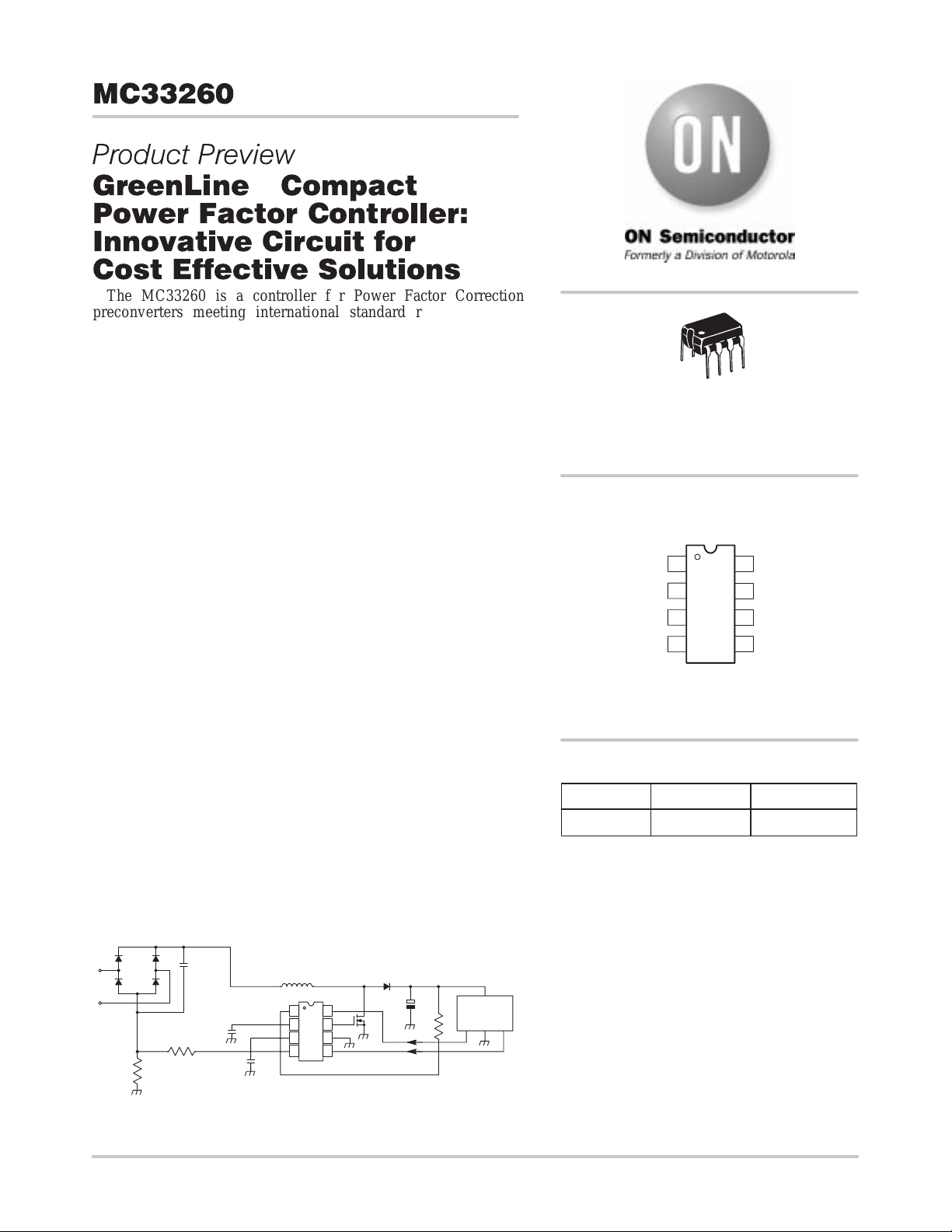
The MC33260 is a controller for Power Factor Correction
preconverters meeting international standard requirements in
electronic ballast and off–line power conversion applications.
Designed to drive a free frequency discontinuous mode, it can also be
synchronized and in any case, it features very effective protections that
ensure a safe and reliable operation.
This circuit is also optimized to offer extremely compact and cost
effective PFC solutions. While it requires a minimum number of
external components, the MC33260 can control the follower boost
operation that is an innovative mode allowing a drastic size reduction
of both the inductor and the power switch. Ultimately, the solution
system cost is significantly lowered.
Also able to function in a traditional way (constant output voltage
regulation level), any intermediary solutions can be easily
implemented. This flexibility makes it ideal to optimally cope with a
wide range of applications.
General Features
• Standard Constant Output Voltage or “Follower Boost” Mode
• Switch Mode Operation: Voltage Mode
• Latching PWM for Cycle–by–Cycle On–Time Control
• Constant On–Time Operation That Saves the Use of an Extra Multiplier
• Totem Pole Output Gate Drive
• Undervoltage Lockout with Hysteresis
• Low Start–Up and Operating Current
• Improved Regulation Block Dynamic Behavior
• Synchronization Capability
• Internally Trimmed Reference Current Source
Safety Features
• Overvoltage Protection: Output Overvoltage Detection
• Undervoltage Protection: Protection Against Open Loop
• Effective Zero Current Detection
• Accurate and Adjustable Maximum On–Time Limitation
• Overcurrent Protection
• ESD Protection on Each Pin
http://onsemi.com
8
1
DIP–8
P SUFFIX
CASE 626
PIN CONNECTIONS AND
MARKING DIAGRAM
AWL
YYWW
V
CC
Gate Drive
7
Gnd
6
Synchronization
5
Input
Feedback Input
V
control
Oscillator
Capacitor (CT)
Current Sense
Input
AWL = Manufacturing Code
18
2
3
MC33260
4
YYWW = Date Code
(Top View)
ORDERING INFORMATION
Device Package Shipping
MC33260P Plastic DIP–8 50 Units / Rail
TYPICAL APPLICATION
D1...D4
R
cs
This document contains information on a product under development. ON Semiconductor
reserves the right to change or discontinue this product without notice.
Semiconductor Components Industries, LLC, 1999
November, 1999 – Rev. 1
Filtering
Capacitor
V
control
R
OCP
L1
8
1
2
7
3
6
MC33260
4
CT
5
V
Sync
D1
C1
CC
+
M1
LOAD
(SMPS, Lamp
Ballast,...)
R
o
1 Publication Order Number:
MC33260/D
CT
MC33260
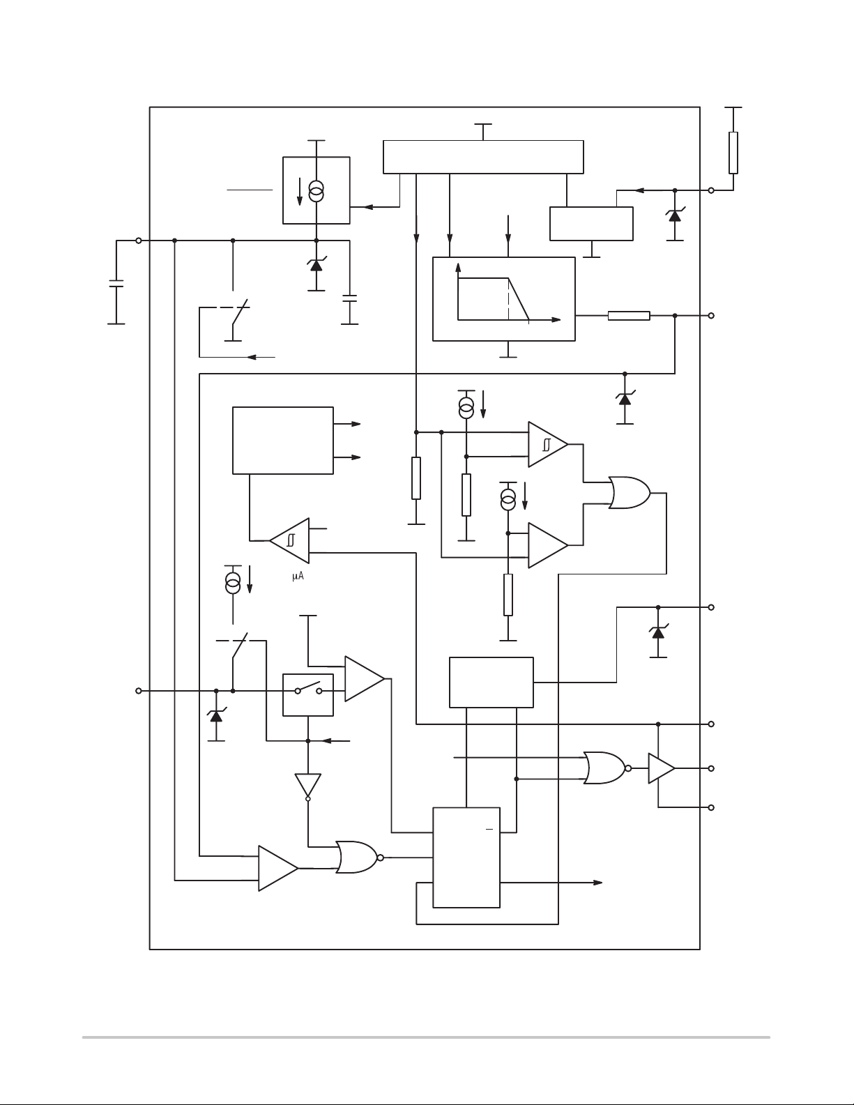
BLOCK DIAGRAM
V
o
Current Mirror
2 x IO x I
I
– ch =
OSC
3
O
I
ref
11 V
I
o
I
oIo
I
ref
V
ref
1.5 V
Current
Mirror
I
o
FB
1
Current
Sense
01
Output_Ctrl
REGULATOR
Enable
–
+
Ics (205 mA)
–60 mV
01
4
11 V
LEB
15 pF
V
ref
I
ref
11 V/8.5 V
+
–
Output_Ctrl
300 k
V
reg
I
o
97%I
r
r
Synchro
Arrangement
I
ref
ref
I
ovpH/IovpL
r
I
+
–
uvp
+
–
11 V
OVP
UVP
11 V
V
control
2
Synchro
5
V
CC
8
+
–
PWM Comparator
ThStdwn
S
R
PWM
R
Latch
RQ
http://onsemi.com
2
Drive
7
Gnd
6
Q
Output_Ctrl
MC33260
MC33260
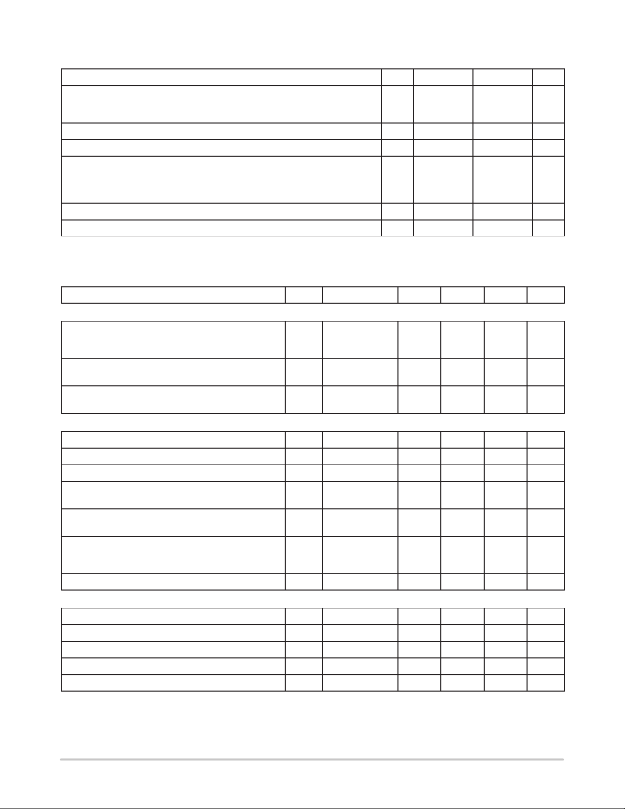
MAXIMUM RATINGS
Rating Pin # Symbol Value Unit
Gate Drive Current (Pin 7)*
Source
Sink
VCC (Pin 8) Maximum Voltage 8 (Vcc)
Input Voltage V
Power Dissipation and Thermal Characteristics
P Suffix, DIP Package
Maximum Power Dissipation @ TA = 85°C
Thermal Resistance Junction to Air
Operating Junction Temperature T
Operating Ambient Temperature T
*The maximum package power dissipation must be observed.
7
I
O(Source)
I
O(Sink)
max
in
P
D
R
θJA
J
A
–500
500
16 V
–0.3 to +10 V
600
100
150 °C
–40 to +105 °C
mA
mW
°C/W
ELECTRICAL CHARACTERISTICS (V
unless otherwise noted.)
Characteristic
GATE DRIVE SECTION
Gate Drive Resistor
Source Resistor @ I
Sink Resistor @ I
Gate Drive Voltage Rise Time (From 3 V Up to 9 V)
(Note 1)
Output Voltage Falling Time (From 9 V Down to 3 V)
(Note 1)
OSCILLATOR SECTION
Maximum Oscillator Swing 3 ∆V
Charge Current @ I
Charge Current @ I
Ratio Multiplier Gain Over Maximum Swing
@ I
=100 µA
pin1
Ratio Multiplier Gain Over Maximum Swing
@ I
=200 µA
pin1
Average Internal Pin 3 Capacitance Over Oscillator
Maximum Swing (V
(Note 2)
Discharge Time (CT = 1 nF) 3 T
REGULATION SECTION
Regulation High Current Reference 1 I
Ratio (Regulation Low Current Reference)/I
Pin 2 Impedance 1 Z
Pin 1 Clamp Voltage @ I
Pin 1 Clamp Voltage @ I
pin1
pin1
= 100 mA
pin7
= 100 mA
pin7
= 100 µA 3 I
= 200 µA 3 I
Varying From 0 Up to 1.5 V)
pin3
= 100 µA 1 V
pin1
= 200 µA 1 V
pin1
= 13 V, TJ = 25°C for typical values, TJ = –40 to 105°C for min/max values
CC
Pin # Symbol Min Typ Max Unit
7
7 t
7 t
3 K
3 K
3 C
reg–H
1 I
reg–L/Ireg–H
R
OL
R
OH
r
f
T
charge
charge
osc
osc
int
disch
reg–H
pin3
pin1–100
pin1–200
10
5
— 50 — ns
— 50 — ns
1.4 1.5 1.6 V
87.5 100 112.5 µA
350 400 450 µA
5600 6400 7200 1/(V.A)
5600 6400 7200 1/(V.A)
10 15 20 pF
— 0.5 1 µs
192 200 208 µA
0.965 0.97 0.98 —
— 300 — kΩ
1.5 2.1 2.5 V
2 2.6 3 V
20
10
35
25
Ω
http://onsemi.com
3
MC33260
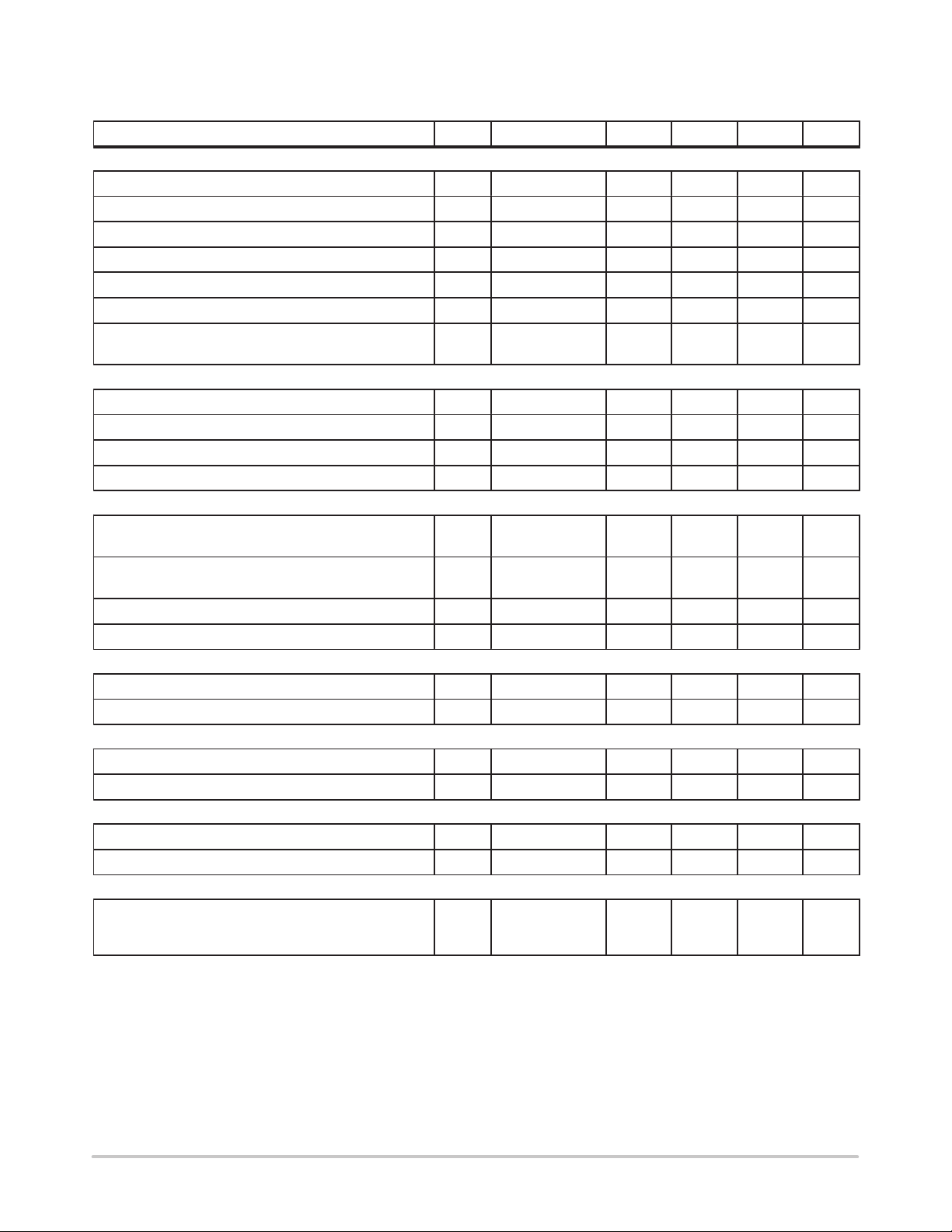
ELECTRICAL CHARACTERISTICS (V
unless otherwise noted.)
Characteristic UnitMaxTypMinSymbolPin #
CURRENT SENSE SECTION
Zero Current Detection Comparator Threshold 4 V
Negative Clamp Level (I
Bias Current @ V
Propagation Delay (V
Pin 4 Internal Current Source 4 I
Leading Edge Blanking Duration τ
OverCurrent Protection Propagation Delay
(Pin 4 < V
SYNCHRONIZATION SECTION
Synchronization Threshold 5 V
Negative Clamp Level (I
Minimum Off–Time 7 T
Minimum Required Synchronization Pulse Duration 5 T
OVERVOLTAGE PROTECTION SECTION
OverVoltage Protection High Current Threshold
and I
reg–H
OverVoltage Protection Low Current Threshold
and I
reg–H
Ratio (I
OVP–H/IOVP–L
Propagation Delay (I
UNDERVOLTAGE PROTECTION SECTION
Ratio (UnderVoltage Protection Current Threshold)/I
Propagation Delay (I
THERMAL SHUTDOWN SECTION
Thermal Shutdown Threshold 7 T
Hysteresis 7 ∆T
VCC UNDERVOLTAGE LOCKOUT SECTION
Start–Up Threshold 8 V
Disable Voltage After Threshold T urn–On 8 V
TOTAL DEVICE
Power Supply Current
Start–Up (VCC = 5 V with VCC Increasing)
Operating @ I
NOTES:
(1) 1 nF being connected between the pin 7 and ground.
(2) Guaranteed by design.
(3) No load is connected to the gate drive which is kept high during the test.
pin4
ZCD–th
Difference
Difference
pin1
= –1 mA) 4 Cl–neg — –0.7 — V
pin2
= V
ZCD–th
> V
pin4
ZCD–th
to Gate Drive Low)
= –1 mA) 5 Cl–neg — –0.7 — V
pin5
) 1 I
pin1
pin1
= 200 µA
> 110% I
< 12% I
to Gate Drive Low) 7 T
ref
to Gate Drive Low) 7 T
ref
= 13 V, TJ = 25°C for typical values, TJ = –40 to 105°C for min/max values
CC
4 I
) to Gate Drive High 7 T
7 T
reg–H
1 I
1 I
1 I
8 I
OVP–H–Ireg–H
OVP–L–Ireg–H
OVP–H/IOVP–L
ZCD–th
b–cs
ZCD
OCP
LEB
OCP
sync–th
off
sync
OVP
UVP/Ireg–H
UVP
stdwn
stdwn
stup–th
disable
CC
–90 –60 –30 mV
–0.2 — — µA
— 500 — ns
192 205 218 µA
— 400 — ns
100 160 240 ns
0.8 1 1.2 V
1.5 2.1 2.7 µs
— — 0.5 µs
8 13 18 µA
0 — — —
1.02 — — —
— 500 — ns
12 14 16 %
— 500 — ns
— 150 — °C
— 30 — °C
9.7 11 12.3 V
7.4 8.5 9.6 V
—
—
0.1
4
0.25
8
mA
http://onsemi.com
4
MC33260
1.6
1.4
1.2
1.0
0.8
control
V : REGULATION BLOCK OUTPUT (V)
0.6
0.4
0.2
0
20
0
60
40
I
pin1
–40°C
25°C
105°C
100
80
: FEEDBACK CURRENT (µA)
120
140
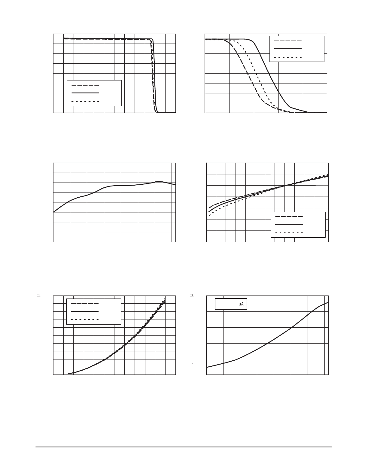
Figure 1. Regulation Block Output versus
Feedback Current
1.340
1.335
1.330
1.325
1.320
1.315
1.310
MAXIMUM OSCILLAT OR SWING (V)I , OSCILLATOR CHARGE CURRENT ( A)
1.305
1.300
–40
–20 0
20
40 60
JUNCTION TEMPERATURE (°C)
160
180
200
80
220
100
240
1.6
1.4
1.2
1.0
0.8
0.6
0.4
0.2
control
V : REGULATION BLOCK OUTPUT (V)
0
185
190 195 200 205 210
I
: FEEDBACK CURRENT (µA)
pin1
Figure 2. Regulation Block Output versus
Feedback Current
3.5
3.0
2.5
2.0
1.5
1.0
FEEDBACK INPUT VOLTAGE (V)
0.5
0
0
20 40 60 80 100 120 140 160 180 200 220 240
I
: FEEDBACK CURRENT (µA)
pin1
–40°C
25°C
105°C
–40°C
25°C
105°C
Figure 3. Maximum Oscillator Swing versus
Temperature
m
500
450
400
350
300
250
200
150
100
50
osc–ch
0
0
20 40 60 80 100 120 140 160 180 200 220 240
I
pin1
–40°C
25°C
105°C
: FEEDBACK CURRENT (µA)
Figure 5. Oscillator Charge Current versus
Feedback Current
Figure 4. Feedback Input Voltage versus
Feedback Current
m
410
I
= 200 mA
pin1
405
400
395
390
385
osc–ch
I , OSCILLATOR CHARGE CURRENT ( A)
–40
–20 0
20
40 60
JUNCTION TEMPERATURE (°C)
Figure 6. Oscillator Charge Current versus
Temperature
80
100
http://onsemi.com
5
MC33260
104
103
102
101
100
99
98
OSCILLATOR CHARGE CURRENT ( A)µ
97
I
= 100 mA
pin1
–40
–20 0 20 40 60 80 100
TJ, JUNCTION TEMPERATURE (°C)
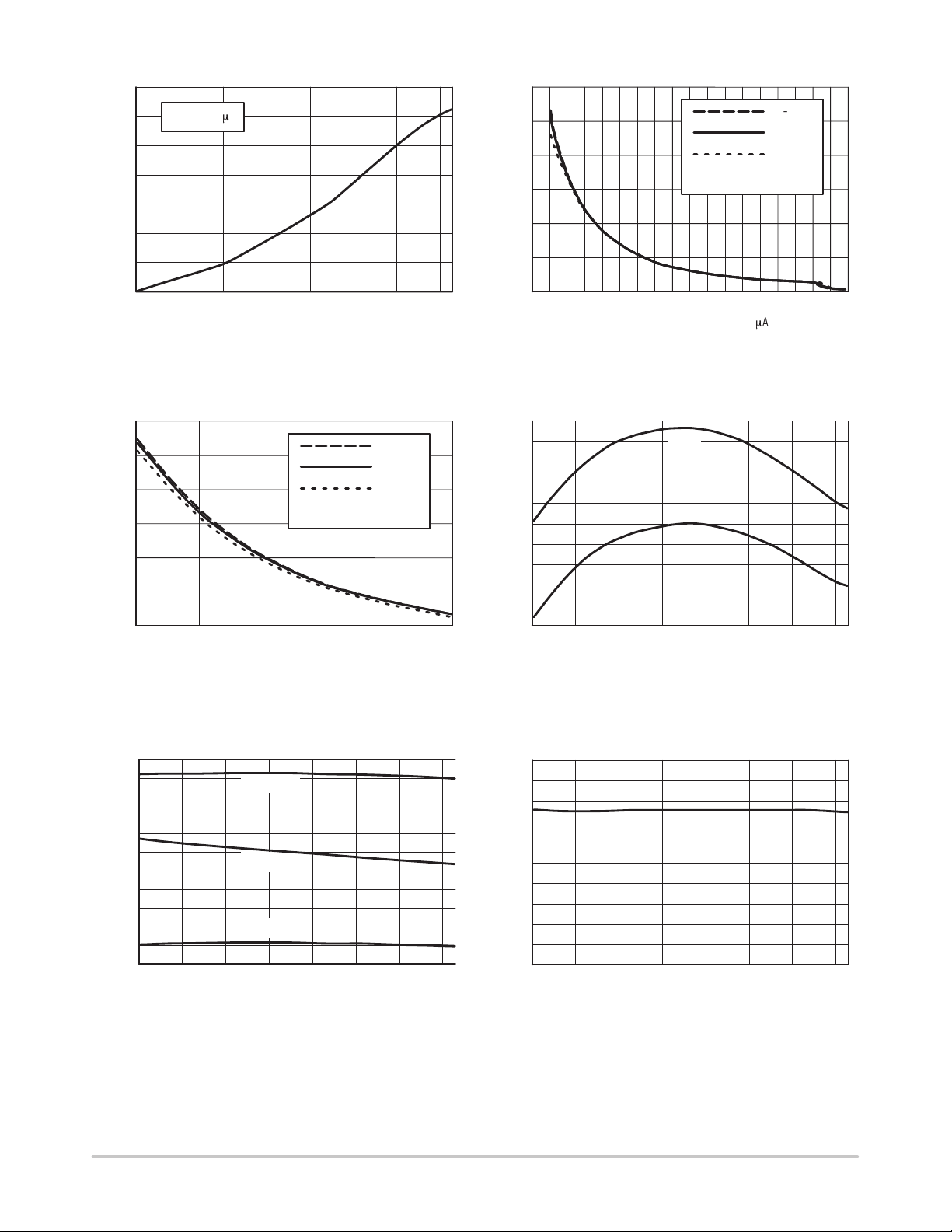
Figure 7. Oscillator Charge Current versus
T emperature
75
65
55
45
ON–TIME ( s)µ
35
25
15
50
60 70 80 90 100
I
: FEEDBACK CURRENT (µA)
pin1
1 nF Connected to Pin 3
–40°C
25°C
105°C
120
100
80
60
ON–TIME ( s)µ
40
20
0
30
50 70 90 110 130 150 170 190 210
I
: FEEDBACK CURRENT (mA)
pin1
1 nF Connected to Pin 3
Figure 8. On–Time versus Feedback Current
207
I
206
205
204
203
202
201
200
199
198
197
REGULATION AND CS CURRENT SOURCE ( A)µ
–20 0 20 40 60 80 100
–40
TJ, JUNCTION TEMPERATURE (°C)
OCP
I
regH
–40°C
25°C
105°C
Figure 9. On–Time versus Feedback Current Figure 10. Internal Current Sources versus
T emperature
1.07
)
1.06
ref
/I
1.05
regL
1.04
), (I
1.03
ref
/I
1.02
1.01
ovpL
1.00
), (I
ref
0.99
/I
0.98
ovpH
(I
0.97
0.96
–40
Figure 11. (I
(I
(I
–20 0 20 40 60 80 100
TJ, JUNCTION TEMPERATURE (°C)
ovpH/Iref
ovpH/Iref
ovpL/Iref
(I
regL/Iref
)
)
)
), (I
ovpL/Iref
), (I
regL/Iref
)
versus T emperature
0.150
0.148
ref
/I )
0.146
uvp
0.144
0.142
0.140
0.138
0.136
0.134
UNDERVOLTAGE RATIO (I
0.132
0.130
–20 0 20 40 60 80 100
–40
TJ, JUNCTION TEMPERATURE (°C)
Figure 12. Undervoltage Ratio versus
T emperature
http://onsemi.com
6
 Loading...