

查询PC33253DW供应商
Freescale Semiconductor, Inc.
Order Number: MC33253/D
Rev 3, 03/2001
nc...
I
cale Semiconductor,
Frees
Advance Information
Full Bridge Pre-Driver
The MC33253 is a full bridge driver including integrated charge
pump, two independent high and low side driver channels.
The high and low side drivers include a cross conduction suppression
circuit, which, if enabled, prevents the external power FETs from being on
at the same time.
The drive outputs are capable to source and sink 1 A pulse peak
current. The low side channel is referenced to ground, the high side
channel is floating above ground.
A linear regulator provides a maximum of 15.5V to supply the low
side gate driver stages. The high side driver stages are supplied with a
10V charge pump voltage. Such built-in feature, associated to external
capacitor provides a full floating high side drive.
An under- and over-voltage protection prevents erratic system
operation at abnormal supply voltages. Under fault, these functions force
the driver stages into off state.
The logic inputs are compatible with standard CMOS or LSTTL
outputs. The input hysteresis makes the output switching time
independent of the input transition time.
The global enable logic signal can be used to disable the charge
pump and all the bias circuit. The net advantage is the reduction of the
quiescent supply current to under 10µA. To wake up the circuit, 5 V has to
be provided at G_EN. A built-in single supply operational amplifier could
be used to feedback information from the output load to the external
MCU.
Operating Voltage Range from 5.5 V up to 55 V
•V
CC
Operating Voltage Range from 5.5 V up to 28 V
•V
CC2
• Automotive Temperature Range -40°C to 125°C
• 1A Pulse Current Output Driver
• Fast PWM Capability
• Built-In Charge Pump
• Cross Conduction Suppression Circuit
V
CC
C2
OUT
CP_
SRC_
HS
GATE_HS
/IN_HS
IN_HS
/IN_LS
IN_LS
GATE_LS
GND1
OUT
LR_
V
CC2
GND_A
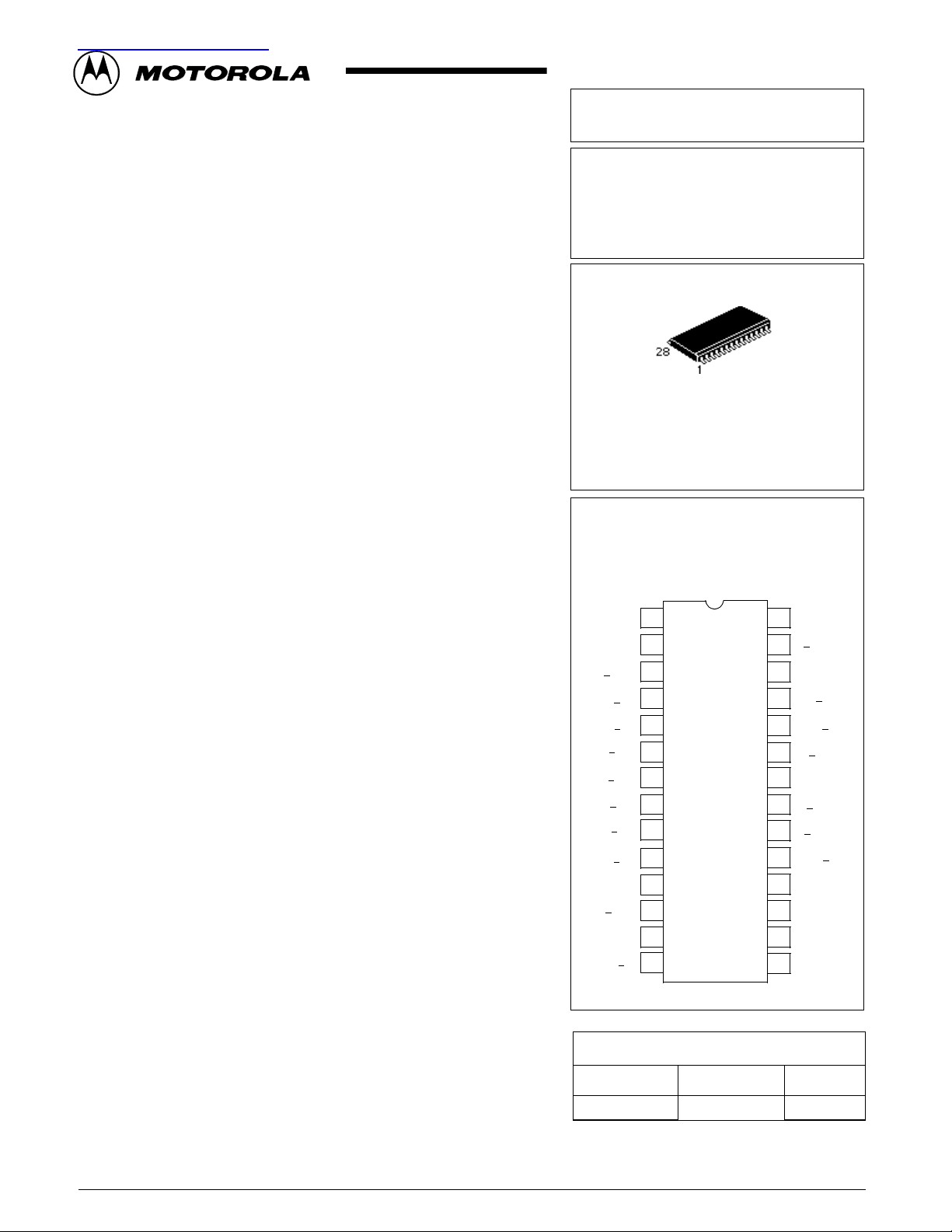
MC33253
55 VOLTS
SEMICONDUCTOR
TECHNICAL DATA
DW SUFFIX
PLASTIC PACKAGE
CASE 751F-05
PIN CONNECTIONS
(TOP VIEW)
CASE 751F-05
1
2
3
4
1
5
1
6
1
7
1
8
1
9
1
10
1
11
12
13
14
28
27
26
25
24
23
22
21
20
19
18
17
16
15
IS
OUT
G_EN
/CCS
SRC_HS
HS
GATE_
/IN_HS
IN_HS
2
/IN_LS
2
IN_LS
2
GATE_LS
GND2
IS
-IN
IS
+IN
C1
2
2
2
2
This document contains information on a new product. Specifications and information herein are
subject to change without notice.
© Motorola, Inc., 2001. All rights reserved.
For More Information On This Product,
Go to: www.freescale.com
ORDERING INFORMATION
Device
PC33253DW
Temperature
Range
Package
SOIC28-40oC to +125oC
Page 1/15
nc...
I
cale Semiconductor,
Frees
G_EN
/CCS
IN_HS1
/IN_HS1
IN_LS1
/IN_LS1
IN_HS2
/IN_HS2
IN_LS2
UV/OV
Detect
Freescale Semiconductor, Inc.
V
CC
V
DD
V
DD
V
DD
V
DD
MC33253
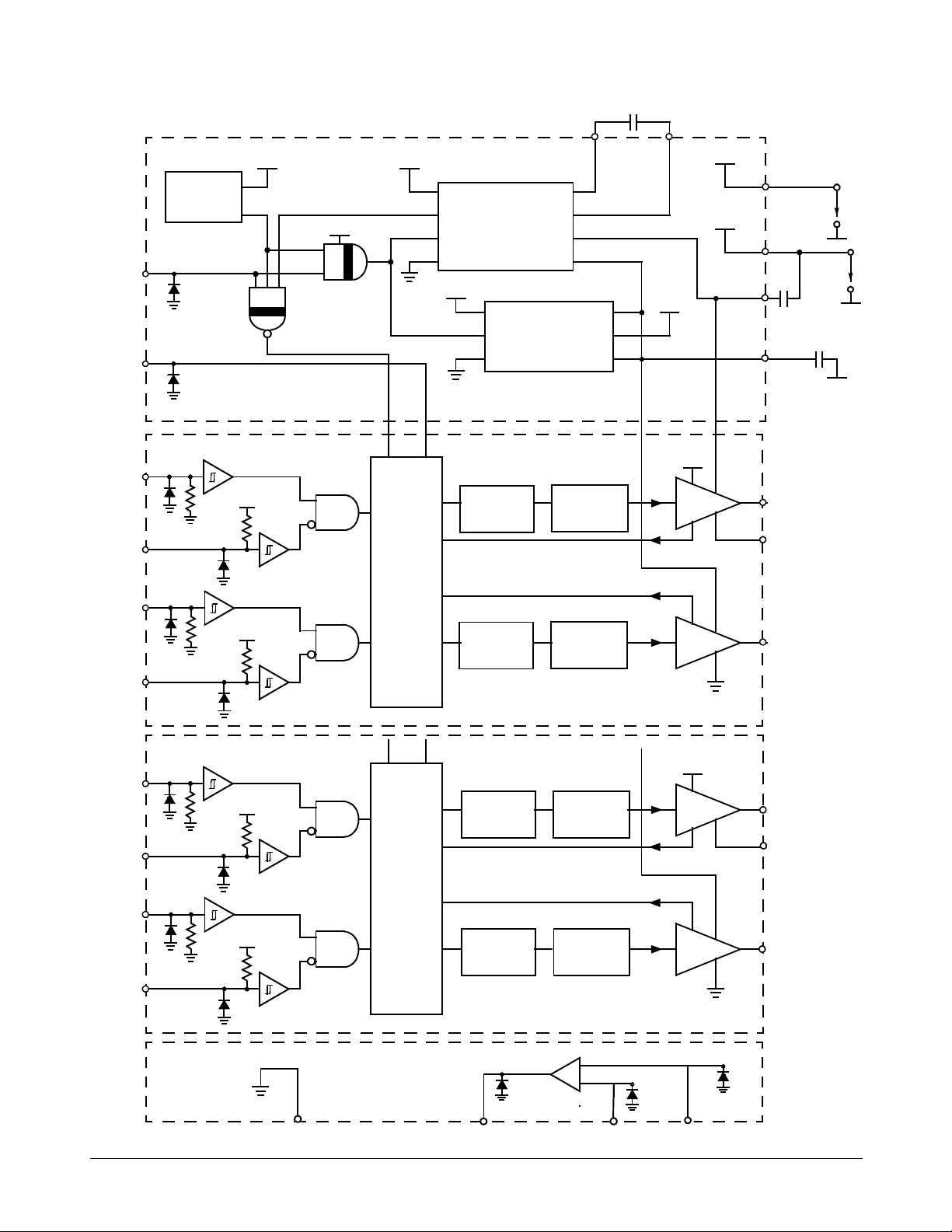
Figure 1. Principal Building Blocks
V
CC
V
CC
RDY
V
DD
BRG_EN CCS
Input
&
CCS
LOGIC
Input
&
CCS
Charge
Pump
EN
GND
V
CC2
V
CC2
EN
GND
HIGH AND LOW SIDE
CONTROL WITH CHARGE PUMP
CCSBRG_EN
VDD/V
POS
Level Shift
VDD/V
CC
Level Shift
HIGH AND LOW SIDE CHANNEL
WITH CROSS CONDUCTION SUPPRESSION
CCSBRG_EN
VDD/V
POS
Level Shift
VDD/V
CC
Level Shift
C1
C2
Vpos
+13.5 V
Linear
Reg
+13.5 V
+5.0 V
+13.5 V
Pulse
Generator
G_LOW_H
G_LOW_LS
Pulse
Generator
Pulse
Generator
G_LOW_H
G_LOW_LS
Pulse
Generator
Ccp
V
DD
Vgs_ls
IN
IN
Vgs_ls
IN
IN
C2C1
V
CC
Output
Driver
Output
Driver
V
CC
Output
Driver
Output
Driver
V
CC2
V
CC2
V
CC
CP_OUT
CP_OUT
LR_OUT
GATE_HS1
SRC_HS1
GATE_LS1
GATE_HS2
SRC_HS2
GATE_LS2
5.5 V...
28 V
5.5 V...
C
LR_OUT
55 V
V
CC
C
Vgs_hsVgs_ls
OUT
OUT
OUT
OUT
/IN_LS2
SENSE CURRENT AMPLIFIER
GND
MC33253 MOTOROLA rev3.0 - 2/15
For More Information On This Product,
HIGH AND LOW SIDE CHANNEL WITH
CROSS CONDUCTION SUPPRESSION
-
CAO
IS
OUT
+
IS
+IN
CA
-
CA
+
IS
-IN
Go to: www.freescale.com
ABSOLUTE MAXIMUM RATINGS Absolute Maximum Ratings indicate sustained limits beyond which damage to the device may occur. All voltage
parameters are absolute voltages referenced to GND.
Rating Symbol Min Max Unit
Freescale Semiconductor, Inc.
MC33253
nc...
I
cale Semiconductor,
Frees
Supply Voltage1 V
Supply Voltage2 (NOTE 1) V
Linear Regulator Output Voltage V
High Side Floating Supply Absolute Voltage V
High Side Floating Source Voltage V
High Side Gate Voltage V
High Side Gate Source Voltage V
High Side Source Current from Cpout in Switch On State I
High Side Floating Supply Gate Voltage V
Low Side Output Voltage V
Wake up Voltage V
Logic Input Voltage V
Charge Pump Capacitor Voltage V
Charge Pump Capacitor Voltage V
Operational Amplifier Output Voltage V
Operational Amplifier Inverting Input Voltage
Operational Amplifier Non Inverting Input Voltage
ESD Voltage on any Pins (HBM, 100pF, 1.5kOhms) V
Power Dissipation and Thermal Characteristics
Maximum Power Dissipation@25°CP
Thermal Resistance Junction-to-Air R
Operating Junction Temperature T
Storage Temperature T
LR_out
CP_OUT
SRC_HS
GATE_HS
GATE_HS
- V
SRC_HS
CP_OUT
- V
GATE_HS
GATE_LS
G_EN
V
V
CC
CC2
S
IN
C1
C2
CAO
CA
CA
ESD
D
θJA
J
stg
-
+
-0.3 65 V
-0.3 35 V
-0.3 18 V
-0.3 65 V
-0.3 65 V
-0.3 65 V
-0.3 20 V
-0.3 65 V
-0.3 17 V
-0.3 35 V
-0.3 10 V
-0.3 V
-0.3 65 V
-0.3 7 V
-0.3 7 V
-0.3 7 V
-2.0 2.0 kV
-40 +150 °C
-65 +150 °C
250 mA
LR_OUT
2W
60 °C/W
V
OPERATING CONDITIONS
Supply Voltage1 V
Supply Voltage2 V
High Side Floating Supply Absolute Voltage V
NOTE1: VCC can sustain load dump pulse 40V, 400ms, 2Ohms
MC33253 MOTOROLA rev3.0 - 3/15
Typical values for TA = 25°C, Min/Max values for TA = -40°C to +125°C
Rating Symbol Min Max Unit
CC
CC2
CP_OUT
5.5 55 V
5.5 28 V
VCC+4 VCC+11but<65 V
For More Information On This Product,
Go to: www.freescale.com
STATIC ELECTRICAL CHARACTERISTICS V
Typical values for TA = 25°C, Min/Max values for TA = -40°C to +125°C, unless otherwise specified.
Characteristics Pin # Symbol Min Typ Max Unit
LOGIC SECTION
Freescale Semiconductor, Inc.
= 12 V, V
CC
MC33253
= 12 V, CCP = 33 nF, G_EN = 4.5 V unless otherwise specified.
CC2
Logic “1” Input Voltage (IN_LS & IN_HS) 7, 9, 20, 22 V
Logic “0” Input Voltage (IN_LS & IN_HS) V
Logic “1” Input Current Vin=5V 7, 9, 20, 22 I
Logic “0” Input Current Vin=0V I
Logic “0” Input Voltage (/IN_LS & /IN_HS&/CCS) 6, 8, 21, 23,
Logic “1” Input Voltage (/IN_LS & /IN_HS&/CCS) V
Logic “0” Input Current Vin=5V 6, 8, 21, 23,
Logic “1” Input Current Vin=0V I
Wake Up Input Voltage (G_EN) 27 V
Wake Up Current (G_EN) VG_EN = 14 V 27 I
nc...
I
cale Semiconductor,
Frees
LINEAR REGULATOR SECTION
Linear Regulator
V
0mA to 20mA
Linear Regulator
V
V
Charge Pump Output Voltage, referenced to V
Charge Pump Output Voltage, referenced to V
Charge Pump Output Voltage, referenced to V
Charge Pump Output Voltage, referenced to V
Peak current through pin 15under rapid changing
Vcc voltages (see Figure 6)
@ V
LR_OUT
@ V
LR_OUT
@ V
LR_OUT
CHARGE PUMP SECTION
from 16.5 to 28 V, I
CC2
=12 V, I
CC2
=5.5V, I
CC2
I
= 0mA, C
LOAD
I
= 7mA, C
LOAD
= VCC=5.5V
V
CC2
= 0mA, C
I
LOAD
V
= VCC=5.5V
CC2
I
= 7mA, C
LOAD
from
LOAD
= 20mA
LOAD
=TBD, VCC = 5.5V12 TBD V
LOAD
CC
CC
CC
CC
Cpout
Cpout
Cpout
Cpout
=1uF
=1uF
=1uF
=1uF
26
26
12 V
12 V
3V
3V
3V
3V
15 I
IH
IL
in+
in-
V
IH
IL
I
in+
in-
G_EN
G_EN
LR_OUT
LR_OUT
CP_OUT
CP_OUT
CP_OUT
CP_OUT
C1
2.0 10 V
0.8 V
200 1000 uA
200 1000 uA
2.0 10 V
0.8 V
TBD TBD uA
TBD TBD uA
4.5 5.0 V
200 500 uA
13.5 16.5 V
V
-
CC2
1.5
V
LR_OUT
- 2
V
LR_OUT
-3
V
LR_OUT
- TBD
V
LR_OUT-
-TBD
-2.0 2.0 A
CC2
V
V
V
V
V
V
Minimum peak voltage at pin 15under rapid
changing Vcc voltages (see Figure 6)
SUPPLY VOLTAGE SECTION
Quiescent Vcc Supply Current V
Operating Vcc Supply Current
=55V and V
(@V
CC
=12V and V
(@V
CC
Quiescent Vcc2 Supply Current V
CC2
CC2
=28V)
=12V)
MC33253 MOTOROLA rev3.0 - 4/15
=0V 1 TBD uA
G_EN
=0V 13 TBD uA
G_EN
For More Information On This Product,
15 V
1
1
min -1.5 V
C1
TBD
TBD
Go to: www.freescale.com
mA
mA
Characteristics Pin # Symbol Min Typ Max Unit
Operating Vcc2 Supply Current
(@V
=55V and V
CC
=12V and V
(@V
CC
Logic pin inactive (high impedance)
CC2
CC2
=28V)
=12V)
Freescale Semiconductor, Inc.
MC33253
13
13
10
8
mA
Under Voltage Shutdown V
Under Voltage Shutdown V
Over Voltage Shutdown V
Over Voltage Shutdown V
OUTPUT SECTION
Output Sink Resistance (Turned off)
V
GATE_HS
Output Source Resistance (Turned on)
V
CP_OUT
High Side Source Current from Cpout in Switch
On State
nc...
I
Max Voltage (V
INH=1, I
Output Dynamic Range (I
Open Loop Gain (at 25°C) A 50 dB
Input Bias Current 16, 17 I
Input Offset Voltage (at 25°C) V
Input Common Mode Voltage Range ICMR 0 5 V
Common Mode Rejection Ratio CMRR 70 dB
Sink Capability (Vo>1.1V) (Note 3) 28 I
Source Capability (Vo<5V) (Note 3) 28 I
cale Semiconductor,
Gain Bandwidth Product GBW 1.8 MHz
Operational Amplifier Output Voltage, I
Operational Amplifier Output Voltage,
Frees
I
source=500uA
Operational Amplifier Slew Rate (+) SR+ 1 V/us
- V
- V
GATE_HS
Smax
SENSE CURRENT AMPLIFIER SECTION (Internal VCC supply @ 12V)
=1V 3, 4, 5, 10,
SRC_HS
=0.1V
GATE_HS
=200mA
(Note2) 13 UV2 4.6 5.1 5.5 V
CC2
CC
CC
CC2
- V
SRC_HS)
sink/source
,
= 200µA) 28 V
sink=500uA
1UV4.65.15.5V
1 OV 576164 V
13 OV2 29.5 31 32.5 V
R
DS
19, 24, 25
4, 25 I
4, 5, 24, 25
28 V
28 V
R
DS
max 200 mA
S
OH
V
OL
IB
io
sink
source
CAO
CAO
4.7 5.0
-5.0 2.0 5.0 mV
2.0 3.0 mA
2.0 3.0 mA
5V
22.0 Ohms
22.0 Ohms
18 V
300
1.0 uA
0.5 V
V
mV
Operational Amplifier Slew Rate (-) SR- 1 V/us
MC33253 MOTOROLA rev3.0 - 5/15
For More Information On This Product,
Go to: www.freescale.com

Freescale Semiconductor, Inc.
MC33253
DYNAMIC ELECTRICAL CHARACTERISTICS V
Typical values for TA = 25°C, Min/Max values for TA = -40°C to +125°C, unless otherwise specified.
Characteristics Pin # Symbol Min Typ Max Unit
Prop. Delay HS and LS, C
Between 50% Input to 50% Output
(see Figure 2)
Turn On Rise Time, C
10% to 90% (NOTE 4) (see Figure 2)
Turn Off Fall Time, C
10% to 90% (NOTE 4) (see Figure 2)
NOTE 2: Between 4.6V and 5.5V, the device has been a non erroneous behaviour.
NOTE 3: Input overdrive 1V
NOTE 4: Rise time is given by time needed to charge the gate from 1V to 10V (Vice versa for fall time)
nc...
I
NOTE : C
N.B.
Pin15 (C1).
corresponds to a capacitor between GATE_HS and SRC_HS for the high side and between GATE_LS and ground for low side.
load
In some applications a large dV/dt at Pin 2 (C2) due to sudden changes at V
Positive transitions at Pin2 (C2) ;mimimum peak current :
min = 2.0A
I
c1
min = 600ns (see for peak description)
t
c1
load
load
load
=5nF ;
=5nF ;
=5nF;
= 12 V, V
CC
5, 6, 7, 8, 9,
20, 21, 22, 23
5, 10, 19, 24
= 12 V, CCP = 33 nF, G_EN = 4.5 V unless otherwise specified.
CC2
t
PD
200 300 ns
t
r
t
f
can cause a large peak currents flowing through
CC
80 180 ns
80 180 ns
Negative transitions at Pin2 (C2); maximum peak current :
max = 2.0A
I
c1
t
max = 600ns (see for peak description)
c1
Current sourced by Pin 15 (C1) during a large dV/dt will result in a negative voltage at Pin 15; negative transitions at Pin2(C2);
minimum peak voltage:
V
min = -1.5V
c1
t
max = 600ns (see for peak description)
c1
cale Semiconductor,
Frees
Figure 2. Limits of C1 Current&Voltage with Large ValuesdV/dt of Vcc
VCC
I
max
c1
I[C1+C2]
0 A
tc1max
V[LR_OUT]
min
t
C1
I
min
c1
V[C1]
0 V
min
V
c1
MC33253 MOTOROLA rev3.0 - 6/15
For More Information On This Product,
Go to: www.freescale.com

Freescale Semiconductor, Inc.
MC33253
Figure 3. Dynamic Characteristics
/IN_HS
or /IN_LS
50%
IN_HS
or IN_LS
GATE_HS
or GATE_LS
50%
50%
t
pd
10%
t
f
90%
50%
50%
t
pd
90%10%
50%
t
r
Driver Characteristics
nc...
I
Turn-On
For turn-on the current required to charge the gate source capacitor Ciss in the specified time can be calculated as follows:
Peak Current for Rise/Fall Time (tr) and a typical PowerMosFET Gate Charge Qg. IP = Qg/tr = 75 nC/80 ns ª 1.0 A
Turn-Off
The peak current for turn-off can be obtained in the same way as for turn-on. In addition to the dynamic current, required to
turn-off or turn-on the FET, various application related switching scenarios have to be considered:
The output driver sources a peak current of up to 1A for 200 ns to turn on the gate. After 200 ns 100 mA are provided
continuously to maintain the gate charged. The output driver sinks a peak current of up to 1A for 200 ns to turn off the gate. After
200 ns 100 mA are sinked continuously to maintain the gate discharged. In order to withstand high dV/dt spikes a low resistive
path between gate and source is implemented during the off state.
Figure 4. OFF-State Driver Requirement
Flyback Spike charge LS-Gate via C
Charge Current I
trolled Turn-On of Low Side FET
cale Semiconductor,
up to 2.0 A! Uncon-
rss
C
g_hs g_hs g_hs
Frees
C
iss
C
I
rss
V
GATE
g_ls g_ls g_ls g_ls
OFF
rss
rss
V
BAT
Flyback Spike pull down HS-
rss
Drain V
Turn-Off of High Side FET
I
L1
GS
C
LOAD
C
C
OFF
Increase Delayed
rss
iss
rss
Flyback Spike charge LS-Gate via
C
Charge Current I
rss
Delayed Turn-Off of Low Side FET
V
BAT
L1
I
LOAD
OFF
C
rss
C
iss
C
rss
up to 2.0 A!
rss
V
BAT
V
-V
GATE
DRN
L1
Flyback Spike pull down HSDrain V
Turn-On of High Side FET
OFF
g_hs
I
LOAD
Increase Uncontrolled
GS
C
rss
C
iss
C
rss
V
BAT
I
LOAD
L1
C
iss
Driver Requirement: Low
Resistive Gate-Source
Path during OFF-State
Driver Requirement: Low Resistive
Gate Source Path during OFF-State.
High Peak Sink Current Capab.
MC33253 MOTOROLA rev3.0 - 7/15
C
iss
C
iss
Driver Requirement:
High Peak Sink Current Capab.
For More Information On This Product,
C
iss
Driver Requirement: Low Resistive
Gate-Source Path during OFF-State
Go to: www.freescale.com

Freescale Semiconductor, Inc.
Driver Supply
The High Side Driver is supplied from the internal charge pump buffered at CP_OUT. The low-drop regulator provides
approx. 3.5 mA (f
7.0 mA for the low side. (Note: The average current required to switch a gate with a frequency of 100kHz is: Average Current
(Charge Pump) for PWM Frq. (f
and one low side at the same time.)
External capacitors on Charge Pump and on Linear Regulator are necessary to supply high peak current absorbed during
switching. The Low Side Driver is supplied from built in low drop regulator.
Gate Protection
The low side gate is protected by the internal linear regulator, which guarantees that V
V
. Especially when working with the charge pump the voltage at POS_HS can be up to 65V. The high side gate is clamped
GS
internally, in order to avoid a V
The Gate protection does not include a Flyback Voltage Clamp that protects the driver and the external FET from a Flyback
voltage that can appear when driving inductive load.This Flyback voltage can reach high negative voltage values and needs to
be clamped externally.
nc...
I
TMOS Failure Protection
All output driver stages are protected against TMOS failure conditions. If one of the external power FETs is destroyed (Gate
, or Gate = Gnd) the function of the remaining output driver stages is not affected. All output drivers are short circuit
= V
CC
protected against short circuits to ground.
Cross Conduction Suppression
The purpose of the cross conduction suppression is to avoid that high and low side FET are turned on at the same time,
cale Semiconductor,
which prevents the half bridge power FETs of a shoot-through condition. The CCS can be disabled / enabled by an external
signal (/CCS).
- /CCS=0, the cross conduction is not allowed.
- /CCS=1, the cross conduction is allowed.
= 50kHz) per gate. In case of the full bridge that means approximately. 14 mA; 7.0 mA for the high side and
PWM
) and ICP = Qg*f
PWM
exceeding 14V.
GS
Figure 5. Gate Protection and Flyback Voltage Clamp
V
gs_ls
IN
Output
Driver
G_LOW
G_LOW
IN
Output
Driver
PWM
MC33253
= 75 nC*100 kHz = 7.5mA. A full bridge application switch only one high side
does not exceed the maximum
GATE_LS
V
gs_hs
V
CC
VGS < 14 V
under all
conditions
Inductive
Flyback Voltage
Clamp
OUT
OUT
GATE_HS
SRC_HS
D
cl
GATE_LS
M
1
L
1
M
2
Frees
MC33253 MOTOROLA rev3.0 - 8/15
For More Information On This Product,
Go to: www.freescale.com

Freescale Semiconductor, Inc.
Figure 6. Input Logic and Cross Conduction Suppression
MC33253
G_EN
AND
/CCS
BRG_EN
IN_HS
/IN_HS
nc...
I
IN_LS
/IN_LS
10 k
AND
10 k
10 k
AND
AND
EN_CP/LDO
UV_OV
RDY
CCS
AND
AND
“1” Enable Charge Pump and LDO
“1” Supply is ok
{
“1” Charge Pump is Ready
“0” Cross Conduction Suppression is Enabled
en2hs = G_LOW_LS, en2ls = G_LOW_HS
“1” Cross Conduction Suppression is Disabled
en2hs = “1”, en2ls = “1” en1hs = “0”, en1ls = “0”
OUT_HS
en2_hs
en2_ls
drv_ls
AND
“1” Turn-On FET
G_LOW_H
“1” FET is Turned-Off
G_LOW_LS
“1” FET is Turned-Off
OUT_LS
AND
“1” Turn-On FET
en1_hs
OR
OR
en1_ls
Logic Inputs
Logic Input Voltage Range:
Absolute Max :
-0.3 V ... 10 V
Wake Up Function:
(G_EN)
4.5 V ... V
During Wake-Up the logic is supplied from the G_EN pin.
Low Drop Linear Regulator
cale Semiconductor,
Frees
The low drop linear regulator provides the 5.0 V for the logic section of the driver, the V
charge pump, which generates the V
exceeds 14.5V the output is limited to 14V.
Charge Pump
The charge pump generates the high side driver supply voltage ( V
charge pump without load:
CC2
buffered at LR_OUT and the +13.5 V for the
CP_OUT
gs_ls
. The basic circuit (Fig 7), shows
CP_OUT
. The low drop linear regulator provides 3.5 mA average current per driver stage. If typically V
gs_hs
), buffered at C
gs_hs
Figure 7. Charge Pump Basic Circuit
V
Ccp_out
Vbat
V
LR_OUT
Osc.
Ccp
(2)
D1
A
D2
(1)
CC2
When the oscillator is in low state (1), Ccp is charged through D2 until its voltage reaches V
state (2), C
the MC33253 oscillator is about 330 kHz.
MC33253 MOTOROLA rev3.0 - 9/15
is discharged though D1 in C
cp
, and final voltage of the charge pump, V
cp_out
cp_out
is V
For More Information On This Product,
. When the oscillator is in high
bat-Vd2
bat+VLR_OUT
- 2Vd. The frequency of
Go to: www.freescale.com

z
Freescale Semiconductor, Inc.
The Figure 8 represents a simplified circuitry of the high side gate driver.
V
LR-OUT
Tosc2
Tosc1
T1
Figure 8. High Side Gate Driver
Ccp
C1
C2
GATE_HS
MC33253
CP_out
D1
D2
Vcc
(3)
Ccp_out
HS
MOSFET
SRC_HS
20KhZ
100 KhZ
Rg
cp_out
LS
MOSFET
Versus Ccp
21.5
21
20.5
20
19.5
Vcp_out (V)
19
18.5
5 25456585
M
provides peak current to the HS MOSFET
cp_out
20kHz
100kH
Ccp (nF)
T2
nc...
I
pins
The transistors Tosc1 and Tosc2 are the oscillator switching MOSFETs. When Tosc1 is on, the oscillator is at low level. When
Tosc2 is on, the oscillator is at high level. The high side MOSFET predriver is composed of two transistors T1 and T2. When T1 is on
the HS MOSFET is turn on, when T2 is on the HS MOSFET is off. The capacitor C
through T1 during turn on (3) as shown in figure 11.
C
cp
C
choice depends on Power MOSFET characteristics and the working switching frequency. The following diagrams show the
cp
influence of C
(MTP60N06HD and MPT36N06V).
cale Semiconductor,
value on V
cp
average voltage level. The diagrams are given at two different frequencies for two power MOSFETs
cp_out
Figure 9. V
Frees
21
20.5
20
19.5
19
Vcp_out (v)
18.5
18
5 25456585
Ccp ( nF)
MTP60N06HD (Qg=50nC)
Figure 10.
MC33253 MOTOROLA rev3.0 - 10/15
For More Information On This Product,
MTP36N06V (Qg=40nC)
Go to: www.freescale.com

Freescale Semiconductor, Inc.
The smaller Ccp value is, the smaller V
increases, the average V
C
cp_out
As shown in figure 11, at high side MOSFET turn on, V
value as following :
C
cp_out
: Power MosFET Gate Charge
Q
g
level decreases. For most of the applications a typical value of 33nF is recommended.
cp_out
cp_out
MC33253
value is. Moreover, for a same C
voltage decreases. This decrease can be calculated according to
cp_out
Q
g
V
=∆
outCcp
_
C
outcp
_
value, when the switching frequency
cp
The following figure is the simplified C
f
: working switching frequency
pwm
Figure 11. Simplified C
Oscillator
V
Cp_out
nc...
I
average V
I
Cp_out
Cp_out
in high
state
cale Semiconductor,
LR_OUT
C
LR_OUT
provides peak current needed by the low side MOSFET turn on. V
C
current and voltage waveforms.
cp_out
Current and Voltage Waveforms
cp_out
Oscillator
in low
state
f=330kHz
Peak
Current
∆
High Side
turn on
outCcpV_
f
PWM
decreasing is as follow:
LR_OUT
Frees
V
outLR
_
Capacitors typical values
In most working cases the following typical values are advised for a good charge pump performing:
=33nF, C
C
cp
These values give a typical 100mV voltage ripple on V
OP-Amp
The built-in A.O.P. available in the MC33253 allows to get a voltage image of the H-bridge current. This voltage can be
provided by a shunt resistor, as shown in figure 13.
Typically shunt resistivity is dimensioned as low as possible (25mOhm/10A). The maximum A.O.P output voltage is 5V.
Therefore a gain of 10 sets the maximum drop voltage on the sensing resistance at 500mV.
MC33253 MOTOROLA rev3.0 - 11/15
=470nF and C
cp_out
=470nF.
LR_OUT
cp_out
For More Information On This Product,
=∆
C
and V
Q
g
outLR
_
LR_OUT
with Qg=50nC.
Go to: www.freescale.com

R
A differential mode is advised as shown in fig 12:
nc...
I
Freescale Semiconductor, Inc.
with R2=R4 and R1=R3, )12(
Figure 12. : Differential A.O.P
V
2
V
1
A gain of 10 gives 10
R
3
MC33253
R
4
R
1
IS
+IN
IS
-IN
IS
AOP
out
=
R
2
OUT
2
R
1
R
( a )
V
out
VV
−=
+
_
V
2
R
1
cale Semiconductor,
Frees
To minimize the perturbations, impedance seen by the A.O.P inputs may be as low as possible.
Knowing the maximum output current (2mA), the minimum value of (R1+R2) can be deduced when V
V
RR 5,2
)(
with (a) and (b), the minimum values of R1, R2, R3 and R4 can be calculated.
R1=R3=227 Ohms and R2=R4=2.27 kOhms
Over/Under Voltage Shutdown
The under voltage protection becomes active at V
at V
above 28 V. If the O/UV protection is activated the outputs are driven low, in order to switch off the FETs.
CC2
Protection
A protection against double battery and load dump spikes up to 55 V is given by V
polarity is given by the external power FET with the free wheeling diodes, forming a conducting pass from ground to V
additional protection is not provided within the circuit. There is a temperature shut down protection per each half bridge. It protects
the circuitry against temperature damage by blocking the output drives.
CC
5
2
==+
mA
min21
below 5.5 V and the overvoltage protection is activated at VCC above 55 V or
( b )
k
= 55 V. A protection against reverse
CC
maximum is 5V:
OUT
CC
. An
MC33253 MOTOROLA rev3.0 - 12/15
For More Information On This Product,
Go to: www.freescale.com

Freescale Semiconductor, Inc.
Figure 13. DC Motor Control with Microcontroller
MC33253
V
BAT
V
LOGIC
C
CAN
PWM
1
PWM
2
PWM
3
PWM
4
mC
nc...
I
Cp
33nF
HS_1
LS_1
HS_2
LS_2
CURRENT FDB
VCC/V
/G_EN
IN_HS
IN_LS
IN_HS
IN_LS
ISOUT
CC2
/CCS
C
C2
1
1
1
2
2
FULL
BRIDGE
DRIVER
R
2
C
LR_OUT
CP_OUT
GATE_HS
SRC_HS
GATE_LS
GATE_HS
SRC_HS
GATE_LS
GND
IS
+IN
IS
-IN
LRout
1
1
1
2
2
2
470nF
470nF
C
Pout
50ohms
50ohms
50ohms
R
4
M
1
M
3
M
50ohms
M
2
G
S
L
R
3
R
M
G
sense
4
S
L
This application use the internal charge pump to provide the high side floating voltage. This voltage can be provided by an
external source also.
cale Semiconductor,
Frees
R
1
MC33253 MOTOROLA rev3.0 - 13/15
For More Information On This Product,
Go to: www.freescale.com

Freescale Semiconductor, Inc.
Pin Symbol Pin Description
1V
2 C2 Charge Pump Capacitor
3 CP_OUT Charge Pump Out
4 SRC_HS1 Source 1 Output High Side
5 GATE_HS1 Gate 1 Output High Side
6 /IN_HS1 Neg. Input High Side 1
7 IN_HS1 Pos. Input High Side 1
8 /IN_LS1 Neg. Input Low Side 1
9 IN_LS1 Pos. Input Low Side 1
10 GATE_LS1 Gate 1 Output Low Side
11 GND1 Power Ground
12 LR_OUT Linear Regulator Output
nc...
I
cale Semiconductor,
13 V
14 GND_A Analog Ground (A.O.P)
15 C1 Charge Pump Capacitor
16 IS+ Sense OpAmp Pos. Input
17 IS- Sense OpAmp Neg. Input
18 GND2 Logic Ground 2
19 GATE_LS2 Gate 2 Output Low Side
20 IN_LS2 Pos. Input Low Side 2
21 /IN_LS2 Neg. Input Low Side 2
22 IN_HS2 Pos. Input High Side 2
23 /IN_HS2 Neg. Input High Side 2
24 GATE_HS2 Gate 2 Output High Side
25 SRC_HS2 Source 2 Output High Side
26 /CCS Enable Cross Conduction Suppression
27 G_EN Global Enable
28 IS_OUT Sense Current OpAmp Output
CC
CC2
MC33253
Supply1
Supply 2
Frees
MC33253 MOTOROLA rev3.0 - 14/15
For More Information On This Product,
Go to: www.freescale.com

Freescale Semiconductor, Inc.
nc...
I
cale Semiconductor,
Frees
A
28
E
1
B
D
PIN 1 IDENT
e
B
M
0.025 B
S
A
C
15
M
M
H
0.25 B
14
A
0.10
A1
SEATING
C
S
PLANE
C
NOTES:
1. DIMENSIONS ARE IN MILLIMETERS.
2. INTERPRET DIMENSIONS AND TOLERANCES
PER ASME Y14.5M, 1994.
3. DIMENSIONS D AND E DO NOT INCLUDE
MOLD PROTRUSIONS.
4. MAXIMUM MOLD PROTRUSION 0.015 PER
SIDE.
5. DIMENSION B DOES NOT INCLUDE D AMBAR
PROTRUSION. ALLOWABLE DAMBAR
PROTRUSION SHALL BE 0.13 TOTAL IN
MILLIMETERS
DIM MIN MAX
A
2.35 2.65
A1
0.13 0.29
B
0.35 0.49
C
0.23 0.32
D
L
θ
17.80 18.05
E
e
H
10.05 10.55
L
θ
7.40 7.60
1.27 BSC
0.41 0.90
0 8
°°
CASE 751F-05
ISSUE F
Motorola reserves the right to make changes without further notice to any products herein. Motorola makes no warranty, representation or guarantee regarding the suitability
of its products for any particular purpose, nor does Motorola assume any liability arising out of the application or use of any product or circuit, and specifically disclaims any and all
liability, including without limitation consequential or incidental damages. “Typ ical ” parameters which may be provided in Motorola data sheets and/or specifications can and do
vary in different applications and actual performance may vary over time. All operating parameters, including “Typical” must be validated for each customer application by
customer’s technical experts. Motorola does not convey any license under its patent rights nor the rights of others. Motorola products are not designed, intended, or authorized for
use as components in systems intended for surgical implant into the body, or other applications intended to support or sustain life, or for any application in which the failure of the
Motorola product could create a situation where personal injury or death may occur. Should Buyer purchase or use Motorola products for any such unintended or unauthorized
application, Buyer shall indemnify and hold Motorola and its officers, employees, subsidiaries, affiliates, and distributors harmless against all claims, costs, damages, and
expenses, and reasonable attorney fees arising out of, directly or indirectly, any claim of personal injury or death associated with such unintended or un authorized use, even if
such claim alleges that Motorola was negligent regarding the design or manufacture of the parts. Motorola and are registered trademarks of Motorola, Inc. Motorola, Inc. is
an Equal Employment Opportunity/Affirmative Action Employer.
How to reach us:
USA / EUROPE / Locations Not Listed: Motorola Literature Distribution; JAPAN: Motorola Japan Ltd.; SPS, Technical Information Center, 3-20-1,
P.O. Box 5405, Denver, Colorado 80217. 1-303-675-2140 or 1-800-441-2447 Minami-Azabu, Minato-ku, Tokyo 106-8573 Japan. 81-3-344-3569
Technical Information Center: 1-800-521-6274 ASIA / PACIFIC: Motorola Semiconductors H.K. Ltd.; Silicon Harbour Centre,
2, Dai King Street, Tai Po Industrial Estate, Tai Po, N.T., Hong Kong.
HOME PAGE: http://www.motorola.com/semiconductors
MC33253 MOTOROLA
For More Information On This Product,
852-26668334
MC33253/D
Go to: www.freescale.com
 Loading...