

Motorola MC33218AP, MC33218DW Datasheet

Order this document by MC33218A/D
Device
Operating
Temperature Range
Package
SEMICONDUCTOR
TECHNICAL DATA
DW SUFFIX
PLASTIC PACKAGE
CASE 751E
VOICE SWITCHED
SPEAKERPHONE WITH
µPROCESSOR INTERFACE
PIN CONNECTIONS
ORDERING INFORMATION
MC33218ADW
MC33218AP
TA = – 40° to +85°C
SO–24L
Plastic DIP
24
1
P SUFFIX
PLASTIC PACKAGE
CASE 724
24
1
CP2 1 24
(Top View)
V
CC
2
3
4
5
6
7
8
9
10
11
12
23
22
21
20
19
18
17
16
15
14
13
XDI
CPT
TLI
TLO
V
B
C
T
CD
NC
CPR
RLI
RLO
TAO
MCO
MCI
POR
DR
DATA
CLK
RXI
RXO
RAO
GND
1
MOTOROLA ANALOG IC DEVICE DATA
The Motorola MC33218A Voice Switched Speakerphone Circuit
incorporates the necessary amplifiers, attenuators, level detectors, and
control algorithm to form the heart of a high quality hands–free
speakerphone system. Included are a microphone amplifier with mute,
transmit and receive attenuators, a background monitoring system for both
the transmit and receive paths, and level detectors for each path. An AGC
system reduces the receive gain on long lines where loop current and power
are in short supply. A dial tone detector prevents fading of dial tone. A Chip
Disable pin permits conserving power when the circuit is not in use.
Additionally, the MC33218A has a serial data port which permits
microprocessor control of the receive volume level, microphone mute,
attenuator range, and selection of transmit, receive, idle or normal modes.
The data port can be operated at up to 1.0 MHz.
The MC33218A can be operated from a power supply, or from the
telephone line, requiring typically 4.6 mA. It can be used in conjunction with a
variety of speech networks. Applications include not only speakerphones,
but intercoms and other voice switched devices.
• Supply Voltage Range: 2.7 to 6.5 V
• Attenuator Range: 53 or 27 dB (Selectable)
• 2 Point Sensing with Background Noise Monitor in Each Path
• Microprocessor Port for Control of:
Volume Control (40 dB Range over 16 Levels)
Mute Microphone Amplifier
Force to Receive, Transmit, or Idle Modes
Attenuator Range Selection (27 or 53 dB)
• Chip Disable Pin Powers Down the Entire IC
• 24 Pin Narrow Body (300 mil) DIP and 24 Pin SOIC
This document contains information on a new product. Specifications and information herein are
subject to change without notice.
Motorola, Inc. 1995
Simplified Block Diagram
This device contains 610 active transistors.
Microphone
Transmit
Out
V
B
V
B
V
B
V
B
V
B
BNM
Reg.
Rx Attenuator
MC33218A
V
CC
Tx Attenuator
Attenuator Control
DTD
Speaker
Amplifier
Speaker
CD
Receive
In
BNM
DR
DATA
POR
CLK
Serial
Port
MC33218A
2
MOTOROLA ANALOG IC DEVICE DATA
MAXIMUM RATINGS
Rating Symbol Min Max Unit
Supply Voltage V
CC
–0.5 7.0 Vdc
Any Input V
in
–0.4 VCC + 0.4 Vdc
Maximum Junction Temperature T
J
– +150 °C
Storage Temperature Range T
stg
–65 +150 °C
NOTE: Devices should not be operated at or outside these values. The “Recommended Operating Limits”
provide for actual device operation.
RECOMMENDED OPERATING LIMITS
Characteristic Symbol Min Typ Max Unit
Supply Voltage (Non–AGC Range) V
CC
3.5 – 6.5 Vdc
(AGC Range) 2.7 – 3.5
Maximum Attenuator Input Signal V
in(max)
– – 300 mVrms
Logic Input Voltage (Pins 8, 17–19) V
INL
Vdc
Low 0 – 0.8
High 2.0 – V
CC
Clock and Data Rate (Serial Port) F
DATA
0 – 1.0 MHz
VB Output Current I
VB
– See
Figure 14
– mA
Operating Ambient Temperature Range T
A
–40 – +85 °C
ELECTRICAL CHARACTERISTICS (T
A
= +25°C, VCC = 5.0 V, CD ≤ 0.8 V, unless noted, see Figure 3.)
Characteristic
Symbol Min Typ Max Unit
POWER SUPPLY
Supply Current (Enabled, CD ≤ 0.8, VB Open, See Figure 13) I
CCE
mA
Idle Mode 3.0 4.6 6.0
Tx Mode – 4.6 –
Rx Mode – 5.3 –
Supply Current (Disabled, CD = 2.0 V , VB Open) I
CCD
µA
VCC = 3.0 V – 67 –
VCC = 5.0 V 50 110 170
VCC = 6.5 V – 150 –
VB Output Voltage (IVB = 0, CD = 0) V
B
Vdc
VCC = 2.7 V – 0.9 –
VCC = 5.0 V 2.1 2.2 2.3
VCC = 6.5 V – 3.0 –
VB Output Resistance (IVB ≤ –1.0 mA) R
OVB
– 600 – Ω
PSRR @ VB versus VCC, f = 1.0 KHz, CVB = 100 µF PSRR – 57 – dB
ATTENUATOR CONTROL
CT Voltage (with Respect to VB) VCT – V
B
mV
(Full Range, B5 = 0) Rx Mode (Maximum Volume) – +150 –
(Full Range, B5 = 0) Idle Mode – 0 –
(Full Range, B5 = 0) Tx Mode – –100 –
(Half Range, B5 = 1) Rx Mode (Maximum Volume – +85 –
(Half Range, B5 = 1) Idle Mode – 0 –
(Half Range, B5 = 1) Tx Mode – –35 –
CT Source Current (Switching to Rx Mode) I
CTR
–55 –42 –33 µA
CT Sink Current (Switching to Tx Mode) I
CTT
33 42 55 µA
CT Idle Current I
CTI
–3.0 0 3.0 µA
Dial Tone Detector Threshold (with Respect to VB at RXO) V
DT
–40 –20 –8.0 mV
MC33218A
3
MOTOROLA ANALOG IC DEVICE DATA
ELECTRICAL CHARACTERISTICS (continued) (T
A
= +25°C, VCC = 5.0 V, CD ≤ 0.8 V, unless noted, see Figure 3.)
Characteristic UnitMaxTypMinSymbol
ATTENUATORS
Receive Attenuator Gain (f = 1.0 kHz, Maximum Volume) dB
Full Attenuation Range (B5 = 0)
Rx Mode
G
RXF
3.0 6.7 9.0
Tx Mode G
RXTF
–49 –47 –43
Idle Mode G
RXIF
–28 –25 –22
Range (Rx to Tx Mode) ∆G
RXF
50 53 56
Half Attenuation Range (B5 = 1)
Rx Mode
G
RXH
–10 –7.0 –4.0
Tx Mode G
RXTH
–37 –34 –31
Idle Mode G
RXIH
–28 –25 –22
Range (Rx to Tx Mode) ∆G
RXH
23 27 29
Volume Control Range
(Rx Mode Only, B3–B0 Changed from 0000 to 1111, See Figures 6, 7)
V
CR
dB
Full Range 34 40 46
Half Range – 25 –
AGC Attenuation Range
(VCC = 3.5 to 2.7 V , Receive Mode Only, B3–B0 = 0000, See Figure 8)
G
AGC
dB
Full Range 12 21 28
Half Range – 19 –
Transmit Attenuator Gain (f = 1.0 kHz, Maximum V olume) dB
Full Attenuation Range (B5 = 0)
Tx Mode G
TXF
3.0 6.7 9.0
Rx Mode G
TXRF
–49 –47 –43
Idle Mode G
TXIF
–19 –16 –13
Range (Tx to Rx Mode) ∆G
TXF
50 53 56
Half Attenuation Range (B5 = 1)
Tx Mode G
TXH
–9.0 –6.5 –3.0
Rx Mode G
TXRH
–36 –34 –30
Idle Mode G
TXIH
–19 –16 –13
Range (Tx to Rx Mode) ∆G
TXH
23 27 29
RAO, TAO Output Current Capability I
OATT
– 2.0 – mA
RAO Offset Voltage with Respect to V
B
V
RAO
mVdc
Rx Mode – –50 –
Idle Mode – 0 –
Tx Mode – –2.0 –
TAO Offset Voltage with Respect to V
B
V
TAO
mVdc
Rx Mode – –2.0 –
Idle Mode – –5.0 –
Tx Mode – –50 –
MICROPHONE AMPLIFIER (Pins 21, 22)
Output Offset with Respect to VB (RF = 300 kΩ) MCO
VOS
– –10 – mVdc
Input Bias Current (Pin 21) I
MBIAS
– –30 – nA
Open Loop Gain (f < 100 Hz) A
VOLM
– 80 – dB
Gain Bandwidth GBW
M
– 1.5 – MHz
Maximum Output Voltage Swing (Note 1) V
OMAX
– 350 – mVrms
Maximum Output Current Capability I
OMCO
– 2.0 – mA
MUTING (∆ Gain)
Microphone Amplifier Only (Measured at Pin 22) AMT dB
RF = 300 kΩ – 73 –
RF = 100 kΩ – 64 –
Microphone Amplifier + Transmit Attenuator in Receive Mode
(Measured at Pin 23) RF = 300 kΩ
TMT
95 113 –
dB
NOTE: 1. Output swing is limited by the capability of the transmit attenuator input. See Figure 16.
MC33218A
4
MOTOROLA ANALOG IC DEVICE DATA
ELECTRICAL CHARACTERISTICS (continued)
(TA = +25°C, VCC = 5.0 V, CD ≤ 0.8 V, unless noted, see Figure 3.)
Characteristic UnitMaxTypMinSymbol
MUTING (∆ Gain)
Timing from Data Ready Lo–to–Hi (See Figure 27) µs
To Mute t
MM
– 2.0 –
To Enable t
ENM
– 1.0 –
RECEIVE AMPLIFIER (Pins 15, 16)
Output Offset with Respect to VB (RF = 10 kΩ) RXO
VOS
– –1.3 – mVdc
Input Bias Current (Pin 16) I
RBIAS
– –30 – nA
Open Loop Gain (f < 100 Hz) A
VOLR
– 80 – dB
Gain Bandwidth G
BWR
– 1.5 – MHz
Maximum Output Voltage Swing (Note 2) V
OMAX
– 350 – mVrms
Maximum Output Current Capability I
ORXO
– 2.0 – mA
LEVEL DETECTORS AND BACKGROUND NOISE MONITORS
Tx–Rx Switching Threshold (Pins 4, 11) I
TH
0.8 1.0 1.2 µA/µA
CPR, CPT Output Resistance (for Pulldown) R
CP
– 5.0 – Ω
CPR, CPT Leakage Current I
CPLK
– –0.2 – µA
CPR, CPT Nominal DC Voltage (No Signal) V
CP
– 1.9 – Vdc
TLO, RLO, CP2 Source Current (@ VB – 1.0 V) I
LDOH
– –2.0 – mA
TLO, RLO, CP2 Output Resistance R
LD
– 500 – Ω
TLO, RLO, CP2 Sink Current (@ VB + 1.0 V) I
LDOL
– 2.0 – µA
CD INPUT (Pin 8)
Switching Threshold V
THCD
– 1.5 – Vdc
Input Resistance (Vin = 0.8 V) R
CD
170 235 300 kΩ
Input Current (Vin = 5.0 V) I
CD
– 40 – µA
Timing µs
To Disable t
CD
– 3.0 –
To Enable t
ENC
– See
Figure 26
–
POR INPUT (Pin 20)
Switching Threshold (2.7 V ≤ VCC ≤ 6.5 V) V
THPOR
– 1.2 – Vdc
Nominal DC Voltage (2.7 V ≤ VCC ≤ 6.5 V) V
POR
– 1.5 – Vdc
Effective Resistance (0 V < Vin < 0.5 V) R
POR
70 115 160 kΩ
Input Current I
POR
µA
Vin = 0 V – –40 –
Vin = 5.0 V – 630 –
Timing to Reset (Pin 20 Taken to < 1.2 V) t
POR
– 30 – µs
Minimum Power On Reset Time (See Figure 20) T
MPOR
ms
C = 0.1 µF VCC = 6.5 V – 2.7 –
C = 0.1 µF VCC = 5.0 V – 3.7 –
C = 0.1 µF VCC = 2.7 V – 10.6 –
NOTE: 2. Output swing is limited by the capability of the receive attenuator input. See Figure 16.
MC33218A
5
MOTOROLA ANALOG IC DEVICE DATA
ELECTRICAL CHARACTERISTICS (continued) (T
A
= +25°C, VCC = 5.0 V, CD ≤ 0.8 V, unless noted, see Figure 3.)
Characteristic UnitMaxTypMinSymbol
SERIAL PORT (Pins 17–19)
Switching Threshold V
THSP
– 1.3 – Vdc
Clock Input Current (Pin 17) I
INCK
µA
DR ≤ 0.8 V Vin = 0.9 V 5.6 7.5 12.8
DR ≤ 0.8 V Vin = 5.0 V – 75 –
DR ≥ 2.0 V Vin = 0.6 V 5.2 7.9 13.3
DR ≥ 2.0 V Vin = 5.0 V – 84 –
Data Input Current (Pin 18)
Vin = 0.9 V
Vin = 5.0 V
I
INDA
5.6
–
7.5
75
12.8
–
µA
Data Ready Input Current (Pin 19)
Vin = 0.9 V
Vin = 5.0 V
I
INDR
13.8
–
20
200
36
–
µA
Timing (Minimum Requirements) (See Figure 2) ns
Data Ready Falling Edge to Clock t
1
– 200 –
8th Clock Rising Edge to DR Rising Edge t
2
– 100 –
Data Setup Time t
3
– 100 –
Data Hold Time t
4
– 100 –
Clock High Time t
5
– 200 –
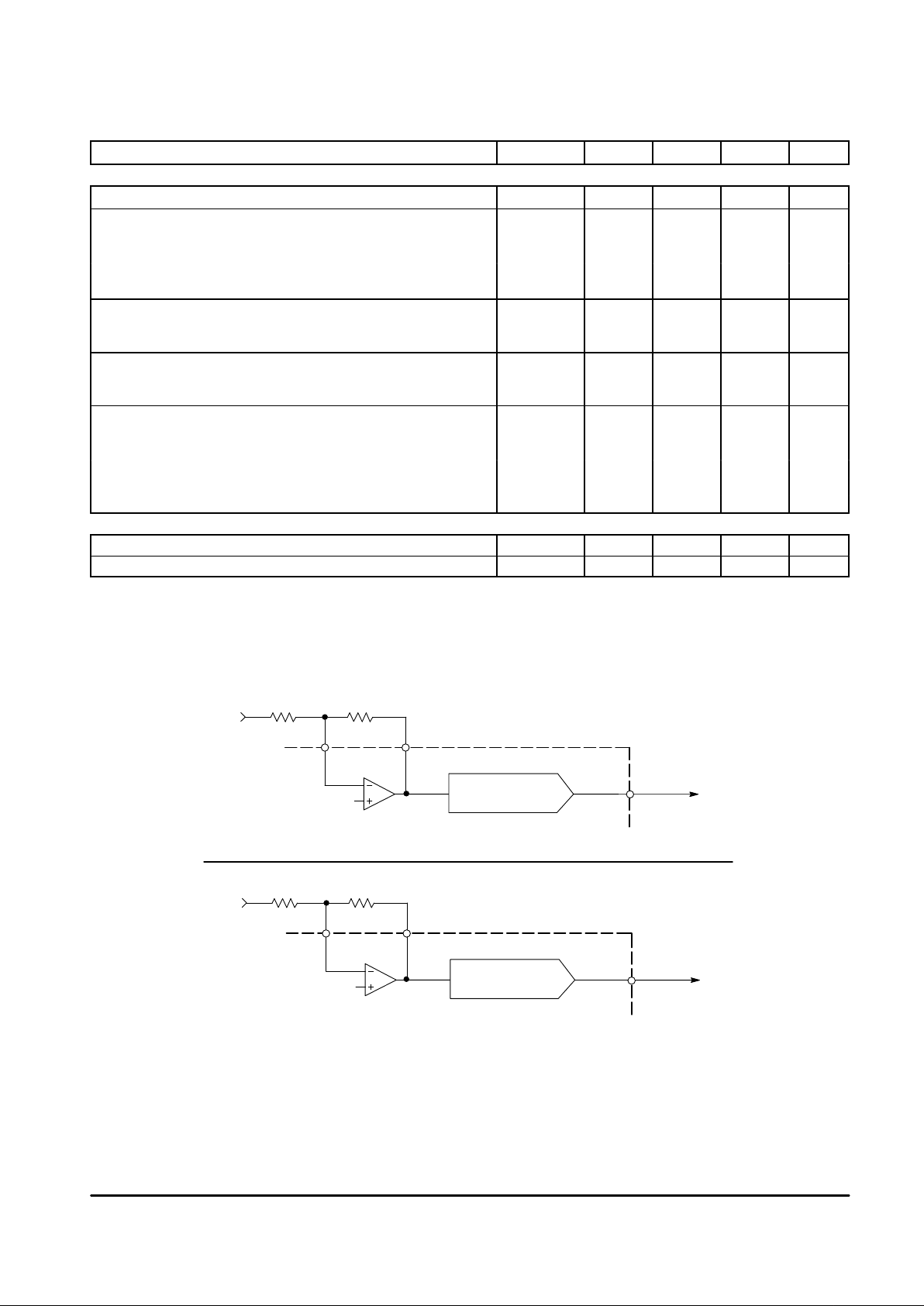
SYSTEM DISTORTION (See Figure 1)
Microphone Amplifier + Tx Attenuator Distortion THD
T
– 0.2 3.0 %
Receive Amplifier + Rx Attenuator Distortion THD
R
– 0.2 3.0 %
Figure 1. System Distortion Test
V
out
V
in
3.5 mV
1.0 kHz
V
B
Tx Attenuator
23
TAO
2221
MCI MCO
3.0 k 300 k
NOTE: Rx Attenuator forced to receive mode.
NOTE: Tx Attenuator forced to transmit mode.
V
out
V
in
350 mV
1.0 kHz
V
B
Rx Attenuator
14
RAO
1516
RXI RXO
10 k 10 k
MC33218A
6
MOTOROLA ANALOG IC DEVICE DATA
TYPICAL TEMPERATURE PERFORMANCE
Characteristics –40°C 0°C +25°C +85°C Unit
Power Supply Current
Enabled, VB Open 5.4 4.9 4.6 4.2 mA
Disabled, VB Open 129 118 110 125 µA
VB Output Voltage (IVB = 0) 2.0 2.15 2.2 2.3 Vdc
CT Source Current (Switching to Rx Mode) –37 –41 –42 –42 µA
CT Sink Current (Switching to Tx Mode) 36 41 42 43 µA
Attenuator “On” Gain (Full Range) 6.7 6.7 6.7 6.4 dB
Attenuator Range (Full Range) 53 53 53 53 dB
Volume Control Range (Rx Mode Only, B3–B0
Changed from 0000 to 1111)
36 39 40 42 dB
AGC Attenuation Range 38 20 21 22 dB
NOTE: Temperature data is typical performance only, based on sample characterization, and does not provide guaranteed limits over temperature.
PIN FUNCTION DESCRIPTION
Pin Symbol
Description
1 CP2 A capacitor at this pin stores voltage representing the transmit background noise and speech levels for the
background noise monitor.
2 XDI Input to the transmit background noise monitor .
3 CPT An RC sets the time constant for the transmit background noise monitor.
4 TLI Input to the transmit level detector.
5 TLO Output of the transmit level detector.
6 V
B
A mid–supply reference voltage, and analog ground for the amplifiers. This must be well bypassed for proper
power supply rejection.
7 C
T
An RC sets the switching time between transmit, receive and idle modes.
8 CD Chip Disable (Logic Input). When low, the IC is active. When high, the entire IC is powered down and
non–functional, except for VB. Input impedance is nominally 235 kΩ.
9 NC No internal connection.
10 CPR An RC sets the time constant for the receive background noise monitor.
11 RLI Input to the receive level detector.
12 RLO Output of the receive level detector.
13 GND Ground pin for the entire IC.
14 RAO Output of the receive attenuator.
15 RXO Output of the receive path input amplifier, and input of the receive attenuator and the dial tone detector.
16 RXI Inverting input of the receive amplifier. Bias current flows out of the pin.
17 CLK Serial Port Clock. 1.0 MHz maximum. Data is entered on clock’s rising edge.
18 DATA Serial Port Data Input. Data consists of an 8 bit word, B7 first, B0 last.
19 DR Serial Port Data Ready. Taking this line high latches new data into the registers.
20 POR Power On Reset for the serial port. Upon power up, or when CD is active, all internal registers are set to logic 0.
This logic input may be taken low to reset the registers.
21 MCI Inverting input of the microphone amplifier. Bias current flows out of the pin.
22 MCO Output of the microphone amplifier, and input of the transmit attenuator.
23 TAO Output of the transmit attenuator.
24 V
CC
Power Supply Pin. Operating Range is 2.7 V to 6.5 Vdc. Bypassing is requried.
MC33218A
7
MOTOROLA ANALOG IC DEVICE DATA
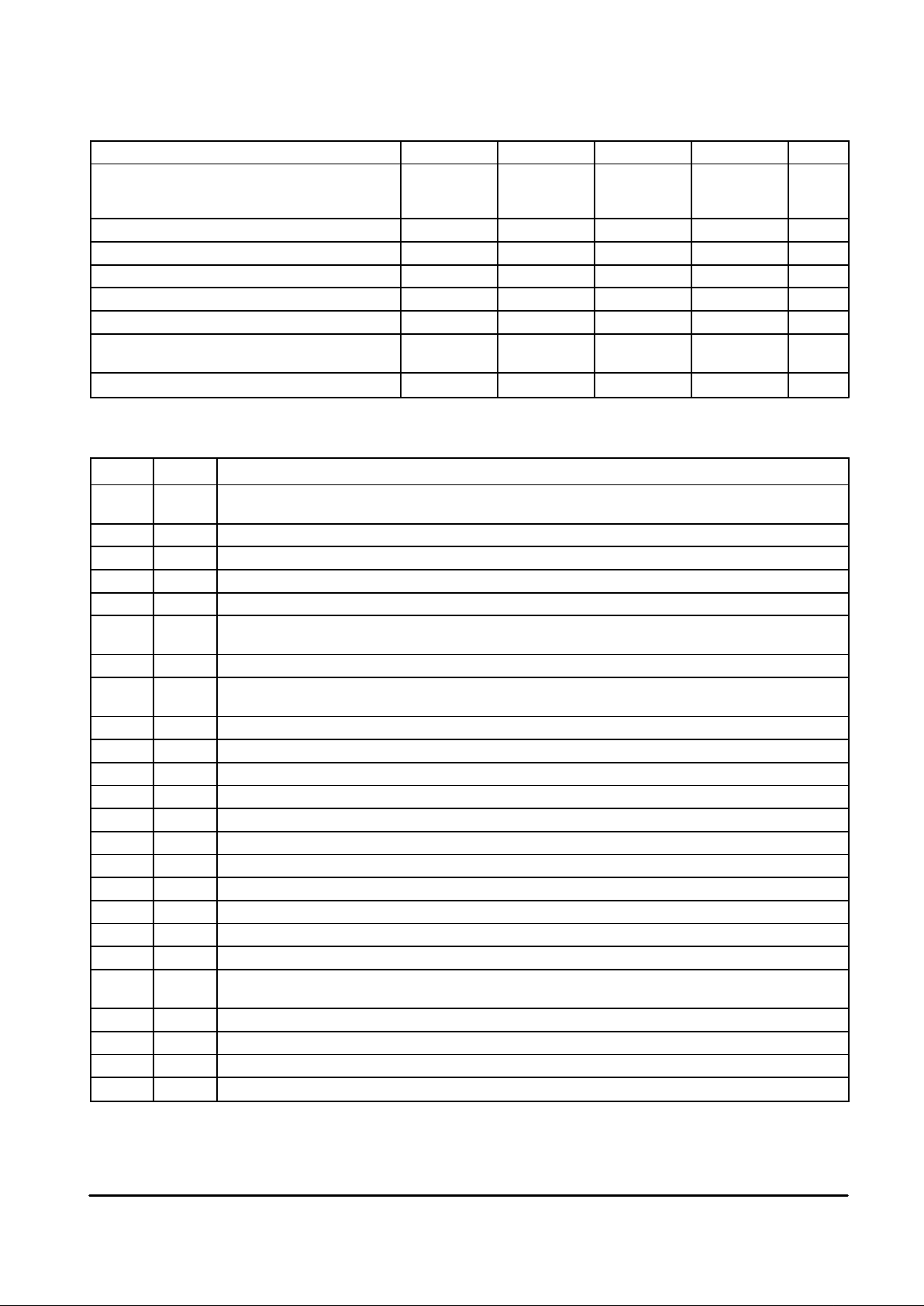
Figure 2. Serial Port Timing Diagram
NOTES: 1. Maximum clock and data rate is 1.0 MHz. There is no required minimum rate.
2.B7 is to be entered first, B0 last.
3.Data is entered on the clock rising edge.
4.Clock can continue to toggle after B0 is entered if Data Ready goes high before the clock’s next rising edge.
This is not recommended due to possible noise problems.
5.Upon power up, all bits are internally set to logic 0, by the POR pin.
6.Data Ready must go low before the first falling clock edge after the clock rising edge associated with B7.
See text for additional information.
B7
t
2
Data Ready
Clock
Data In
t
5
B6 B5 B4 B3 B2 B1 B0
t
1
t3t
4
SERIAL PORT CONTROL BITS
Bits Code Function
B7, B6 00
01
10
11
Normal voice switched operation
Force to receive mode
Force to idle mode
Force to transmit mode
B5 01Attenuator range is 53 dB
Attenuator range is 27 dB
B4 01Microphone amplifier is active
Microphone amplifier is muted
B3–B0
(Note 1)
0000
1111
Maximum receive volume
Minimum receive volume
NOTE: 1. Bit B0 is the LSB for the volume control.
MC33218A
8
MOTOROLA ANALOG IC DEVICE DATA
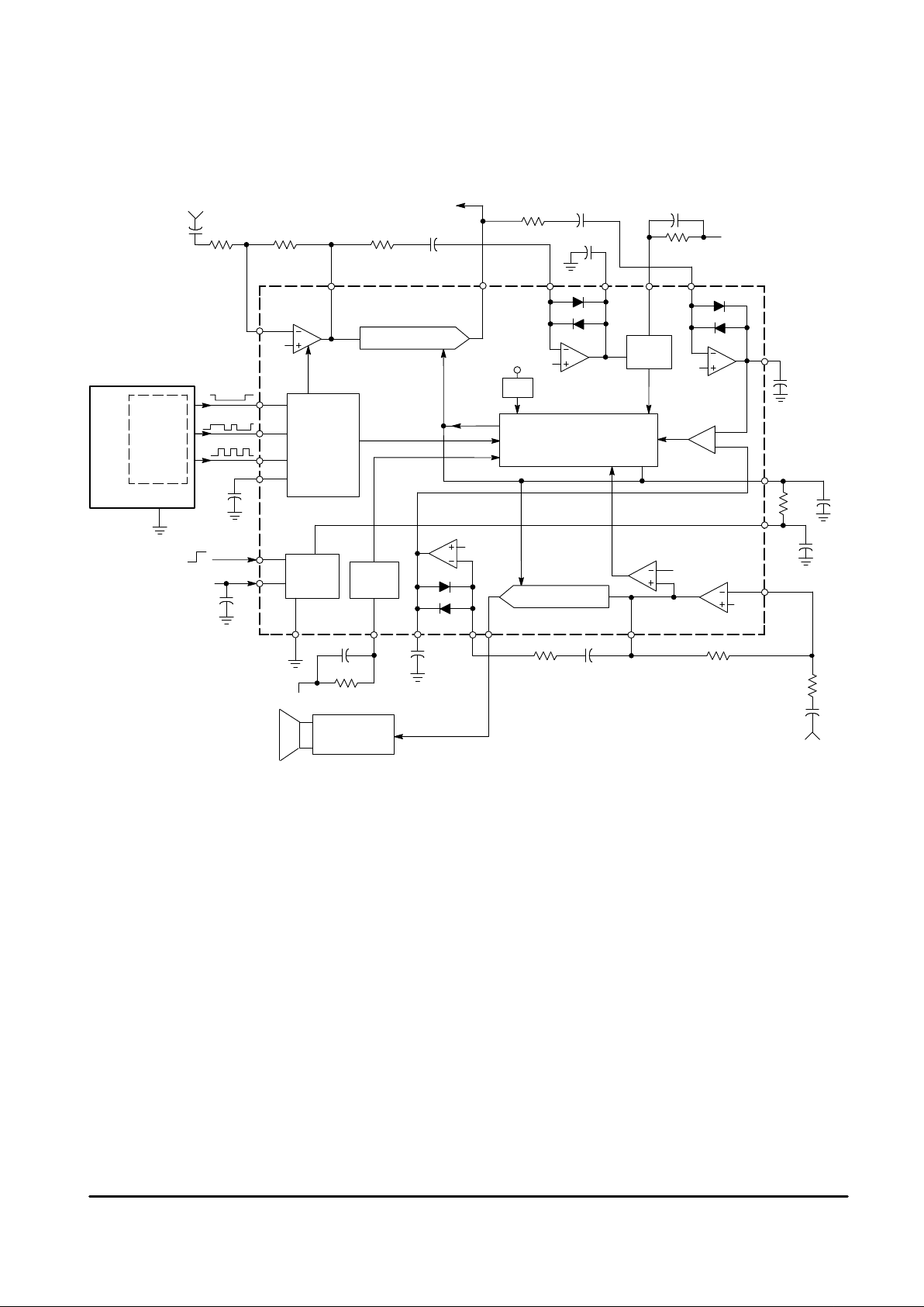
Figure 3. MC33218A Block Diagram and Test Circuit
NOTES: 1. All capacitors are in µF unless otherwise noted.
2.Values shown are suggested initial values only . See Applications Information for circuit adjustments.
MC341 19
Speaker
Amplifier
Receive Input
From 2–4 Wire
Converter
Rx Attenuator
Attenuator Control Circuit
Tx Attenuator
Bias
AGC
T
x
BNM
Dial Tone
Detector
R
x
BNM
0.1
5.1 k
R
2
10 k
10 k
0.1
1.0
47
100 k
V
CC
100
15
15 k
1.0
100
V
B
V
B
V
TH
Microprocessor
DR
Disable
CD
V
CC
0.22
From
Microphone
Transmit Output
To 2–4 Wire Converter
470.14.7 k
0.1
5.1 k
300 k
1.0
100 k
V
CC
VB6
7
5
16
15
14111210
13
24
8
18
21
22
3.0 k
V
B
34
223
1
Tx–Rx Comp.
V
B
V
CC
V
B
Clock
Data
Data
Register
and
Decode
Logic
17
20
19
SPI
Normal
0.1
GND CPR RLO RLI RAO RXO
RXI
CT
TLO
TLICPTCP2TAOMCO XDI
R
1
POR
CK
DIN
DR
MCI
MC33218A
9
MOTOROLA ANALOG IC DEVICE DATA
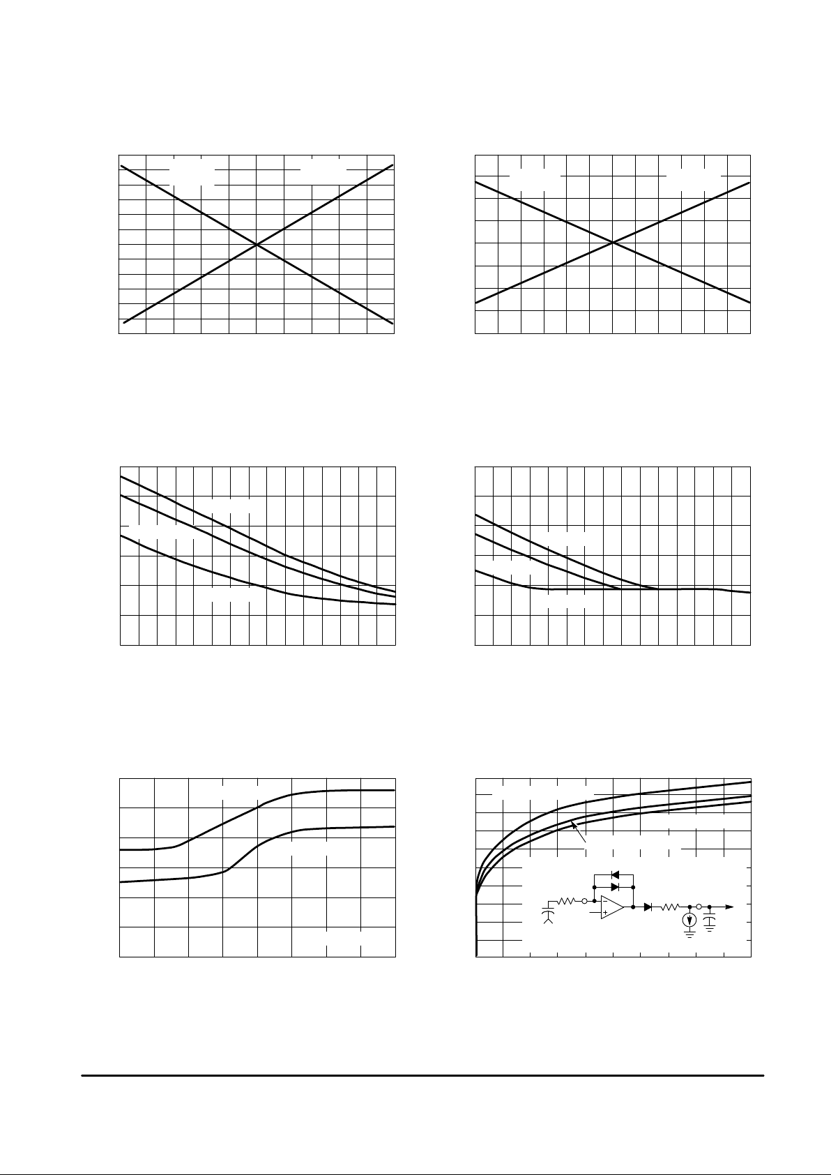
–35
0
–100
10
ATTENUATOR GAIN (dB)
VCT – VB (mV)
ATTENUATOR GAIN (dB)
0–50
50
150100
5.0
8545
0
–10
–20
–30
–40
–10
–20
–30
–40–50
Transmit
Attenuator
Receive
Attenuator
Transmit
Attenuator
Receive
Attenuator
VCT – VB (mV)
0
10
4
8F
C
0
–10
–20
–30
–50
–40
RECEIVE ATTENUATOR GAIN (dB)
VOLUME SETTING (BITS B3–B0, HEX VALUE)
0
10
4
8F
C
0
–10
–20
–30
–50
–40
RECEIVE ATTENUATOR GAIN (dB)
VOLUME SETTING (BITS B3–B0, HEX VALUE)
V
out – B
, OUTPUT VOL TAGE (mV)V
0
100
Vin, INPUT SIGNAL (mVrms)
60
20
0
–60
–20
–100
2.0 µA
V
out
1.0 µF
500
TLI
RLI
XDI
TLO
RLO
CP2
V
in
@ 1.0 kHz
40 80 120 160 200
C
R
2.7
10
2.9
3.1 3.5
3.3
0
–10
–20
–30
–50
–40
RECEIVE ATTENUATOR GAIN (dB)
VCC (Vdc)
Figure 4. Attenuator Gain versus VCT (Pin 7)
(Full Attenuator Range)
Figure 5. Attenuator Gain versus V
CT
(Half Attenuation Range)
Figure 6. Receive Gain versus Volume Control
Levels (Full Attenuation Range)
Figure 7. Receive Gain versus Volume Control
Levels (Half Attenuation Range)
Figure 8. Receive Gain versus V
CC
Figure 9. Level Detector AC
Transfer Characteristics
–15 25
65
VCC ≥ 3.5 V
VCC = 3.1 V
VCC = 2.7 V
VCC ≥ 3.5 V
VCC = 3.1 V
VCC = 2.7 V
Full Range
Half Range
B3–B0 = 0000
R = 5.1 k, C = 0.1 µF
R = 10 k, C = 0.047 µF
R = 10 k, C = 0.1 µF
V
B
 Loading...