Device
Operating
Temperature Range
Package
ORDERING INFORMATION
MC33215FB
MC33215B
T
A
= –20° to +70°C
TQFP–52
SDIP–42
B SUFFIX
PLASTIC PACKAGE
CASE 858
(SDIP–42)
Order this document by MC33215/D
FB SUFFIX
PLASTIC PACKAGE
CASE 848B
(TQFP–52)
52
1
42
1
1
MOTOROLA ANALOG IC DEVICE DATA
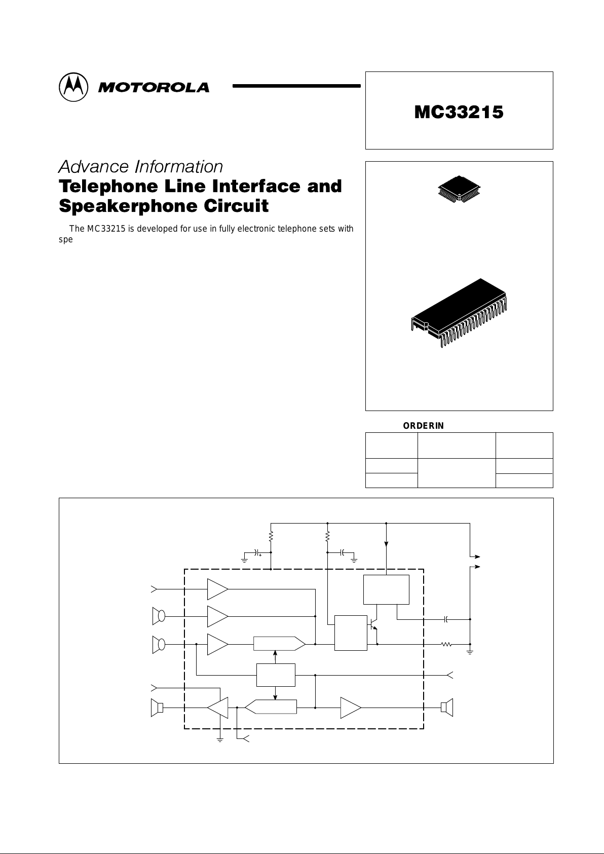
The MC33215 is developed for use in fully electronic telephone sets with
speakerphone functions. The circuit performs the ac and dc line termination,
2–4 wire conversion, line length AGC and DTMF transmission. The
speakerphone part includes a half duplex controller with signal and noise
monitoring, base microphone and loudspeaker amplifiers and an efficient
supply. The circuit is designed to operate at low line currents down to 4.0 mA
enabling parallel operation with a classical telephone set.
• Highly Integrated Cost Effective Solution
• Straightforward AC and DC Parameter Adjustments
• Efficient Supply for Loudspeaker Amplifier and Peripherals
• Stabilized Supply Point for Handset Microphone
• Stabilized Supply Point for Base Microphone
• Loudspeaker Amplifier can be Powered and Used Separately
• Smooth Switch–Over from Handset to Speakerphone Operation
• Adjustable Switching Depth for Handsfree Operation
Simplified Application
This device contains 2782 active transistors.
Attenuator
DTMF
Attenuator
Duplex
Controller
Line
Driver
Current
Splitter
1:10
Handset
Microphone
Base
Microphone
V
CC
or
External Supply
Base Loudspeaker
Auxiliary Input
Handset Earpiece
Receive Signal
Telephone
Line
V
CC
Supply
DC Slope
Line Current
DC Offset
AC
Impedance
R
x
LS
BM
HM
MF
This document contains information on a new product. Specifications and information herein
are subject to change without notice.
Motorola, Inc. 1997 Rev 0
MC33215
2
MOTOROLA ANALOG IC DEVICE DATA
FEATURES
Line Driver and Supply
• AC and DC Termination of Telephone Line
• Adjustable Set Impedance for Real and Complex
Termination
• Efficient Supply Point for Loudspeaker Amplifier and
Peripherals
• Two Stabilized Supply Points for Handset and Base
Microphones
• Separate Supply Arrangement for Handset and
Speakerphone Operation
Handset Operation
• Transmit and Receive Amplifiers
• Differential Microphone Inputs
• Sidetone Cancellation Network
• Line Length AGC
• Microphone and Earpiece Mute
• Separate Input for DTMF and Auxiliary Signals
• Parallel Operation Down to 4.0 mA of Line Current
Speakerphone Operation
• Handsfree Operation via Loudspeaker and Base
Microphone
• Integrated Microphone and Loudspeaker Amplifiers
• Differential Microphone Inputs
• Loudspeaker Amplifier can be Powered and Used
Separately from the Rest of the Circuit
• Integrated Switches for Smooth Switch–Over from
Handset to Speakerphone Operation
• Signal and Background Noise Monitoring in Both
Channels
• Adjustable Switching Depth for Handsfree Operation
•
Switch–Over
• Dial Tone Detector in the Receive Channel
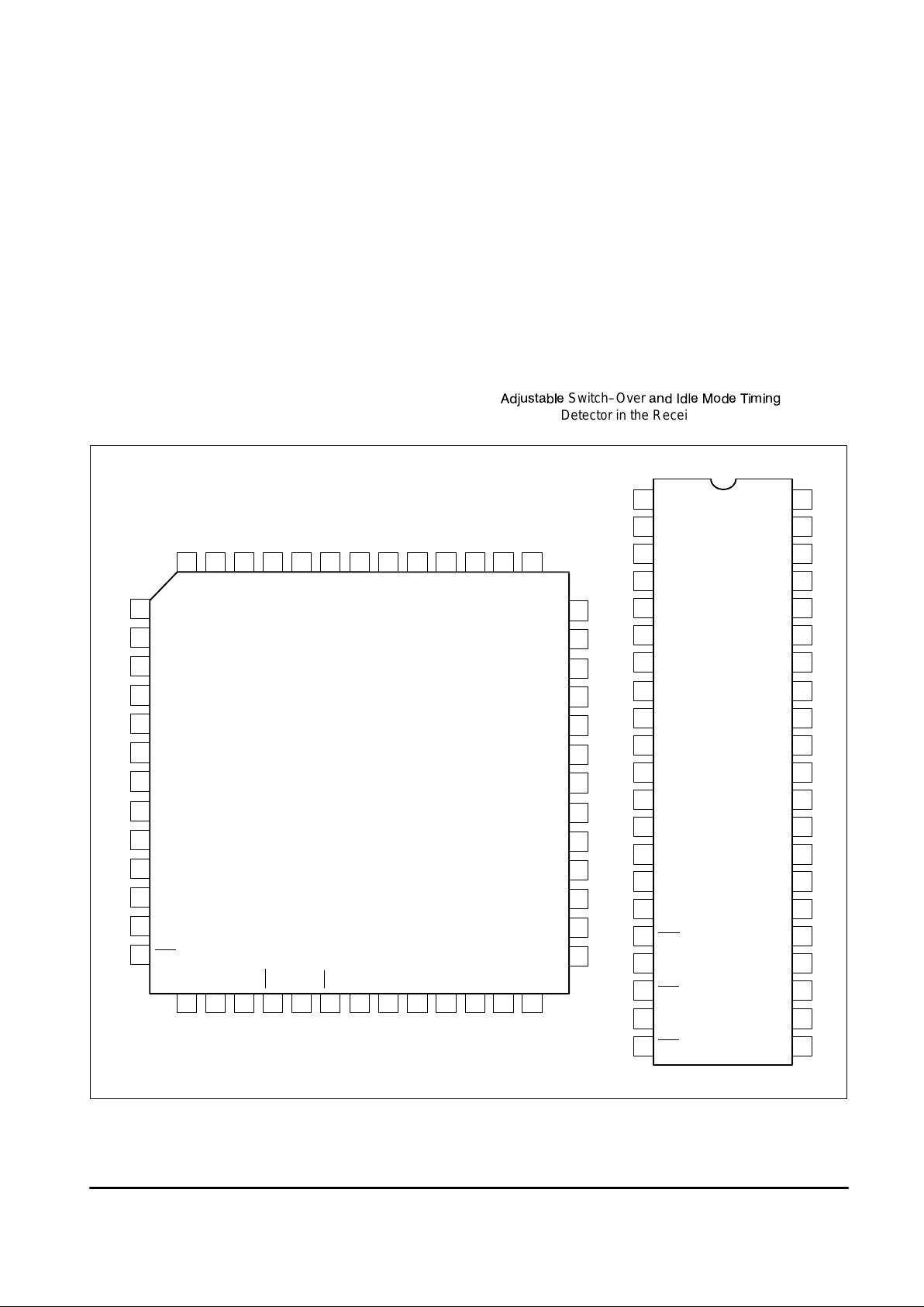
TQFP–52
Figure 1. Pin Connections
1
2
3
4
5
6
7
8
9
10
11
12
13
14
15
16
17
18
19
20
21
42
41
40
39
38
37
36
35
34
33
32
31
30
29
28
27
26
25
24
23
22
1
2
3
4
5
6
7
8
9
10
11
12
13
14 15 16 17 18 19 20 21 22 23 24 25 26
39
38
37
36
35
34
33
32
31
30
29
28
27
52 51 50 49 48 47 46 45 44 43 42 41 40
SLB
REG
SLP
MFI
HM1
HM2
BM2
BM1
V
DD
TSA
TSE
TBN
MUT
LSF
BVO
PPL
LSI
VOL
SWD
REF
AGC
Gnd
RLS
RSA
RSE
RBN
SLB
REG
SLP
MFI
HM1
HM2
BM2
BM1
V
DD
TSA
TSE
TBN
MUT
V
CC
VLN
VHF
VMC
SPS
PRS
SWT
LSM
LSF
BVO
PPL
LSI
VOL
SWD
REF
AGC
Gnd
RLS
RSA
RSE
RBN
RXI
GRX
RXO
RXS
PGD
LSO
VLS
LSB
(Top View)
(Top View)
N/C
N/C
N/C
N/C
SPS
PRS
SWT
LSM
N/C
RXS
RXO
GRX
RXI
N/C
N/C
N/C
N/C
VMC
VHF
VLN
CC
N/C
PGD
LSO
VLS
LSB
V
SDIP–42
MC33215
3
MOTOROLA ANALOG IC DEVICE DATA
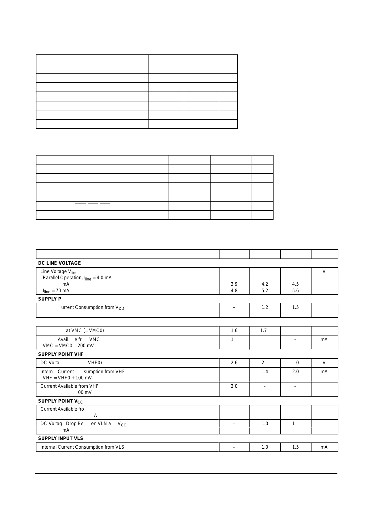
MAXIMUM RATINGS
Rating Min Max Unit
Peak Voltage at VLN –0.5 12 V
Maximum Loop Current – 160 mA
Voltage at VLS (if Powered Separately) –0.5 12 V
Voltage at VHF (if Externally Applied) –0.5 5.5 V
Voltage at SPS, MUT, PRS, LSM –0.5 7.5 V
Maximum Junction Temperature – 150 °C
Storage Temperature Range –65 150 °C
NOTE: ESD data available upon request.
RECOMMENDED OPERATING CONDITIONS
Characteristic Min Max Unit
Biasing Voltage at VLN 2.4 10 V
Loop Current 4.0 130 mA
Voltage at VLS 2.4 8.0 V
Voltage at VHF (if Externally Applied) 2.4 5.0 V
Voltage at SPS, MUT, PRS, LSM 0 5.0 V
Operating Ambient Temperature Range –20 70 °C
ELECTRICAL CHARACTERISTICS (All parameters are specified at T = 25°C, I
line
= 18 mA, VLS = 2.9 V, f = 1000 Hz,
PRS
= high, MUT = high, SPS = low, LSM = high, test figure in Figure 17 with S1 in position 1, unless otherwise stated.)
Characteristic
Min Typ Max Unit
DC LINE VOLTAGE
Line Voltage V
line
ÁÁÁÁ
V
Parallel Operation, I
line
= 4.0 mA – 2.4 –
I
line
= 20 mA
3.9
4.2
4.5
I
line
= 70 mA
4.8
ÁÁÁÁ
5.2
5.6
SUPPLY POINT V
DD
Internal Current Consumption from V
DD
–
ÁÁÁÁ
1.2
1.5
mA
VDD = 2.5 V
SUPPLY POINT VMC
DC Voltage at VMC (= VMC0)
1.6
ÁÁÁÁ
1.75
1.9
V
Current Available from VMC
1.0
ÁÁÁÁ
–
–
mA
VMC = VMC0 – 200 mV
SUPPLY POINT VHF
DC Voltage at VHF (= VHF0)
2.6
ÁÁÁÁ
2.8
3.0
V
Internal Current Consumption from VHF
–
ÁÁÁÁ
1.4
2.0
mA
VHF = VHF0 + 100 mV
Current Available from VHF
2.0
ÁÁÁÁ
–
–
mA
VHF = VHF0 – 300 mV
SUPPLY POINT V
CC
Current Available from V
CC
13
ÁÁÁÁ
15
–
mA
VCC = 2.4 V , I
line
= 20 mA
ÁÁÁÁ
DC Voltage Drop Between VLN and V
CC
–
ÁÁÁÁ
1.0
1.5
V
I
line
= 20 mA
ÁÁÁÁ
SUPPLY INPUT VLS
Internal Current Consumption from VLS
–
ÁÁÁÁ
1.0
1.5
mA
MC33215
4
MOTOROLA ANALOG IC DEVICE DATA
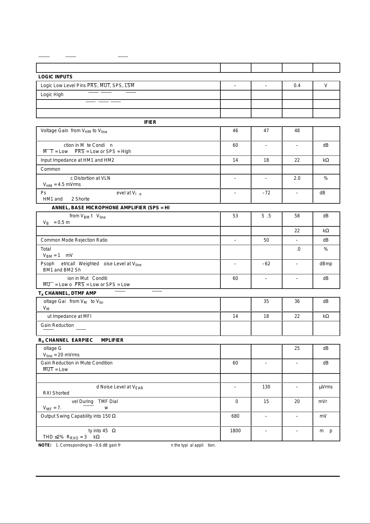
ELECTRICAL CHARACTERISTICS
(continued) (All parameters are specified at T = 25°C, I
line
= 18 mA, VLS = 2.9 V, f = 1000 Hz,
PRS
= high, MUT = high, SPS = low, LSM = high, test figure in Figure 17 with S1 in position 1, unless otherwise stated.)
Characteristic UnitMaxTypMin
LOGIC INPUTS
Logic Low Level Pins PRS, MUT, SPS, LSM – – 0.4 V
Logic High Level Pins PRS, MUT, SPS, LSM 2.0 – 5.0 V
Internal Pull Up Pins PRS, MUT, LSM – 100 – kΩ
Internal Pull Down Pin SPS
–
ÁÁÁÁ
100
–
kΩ
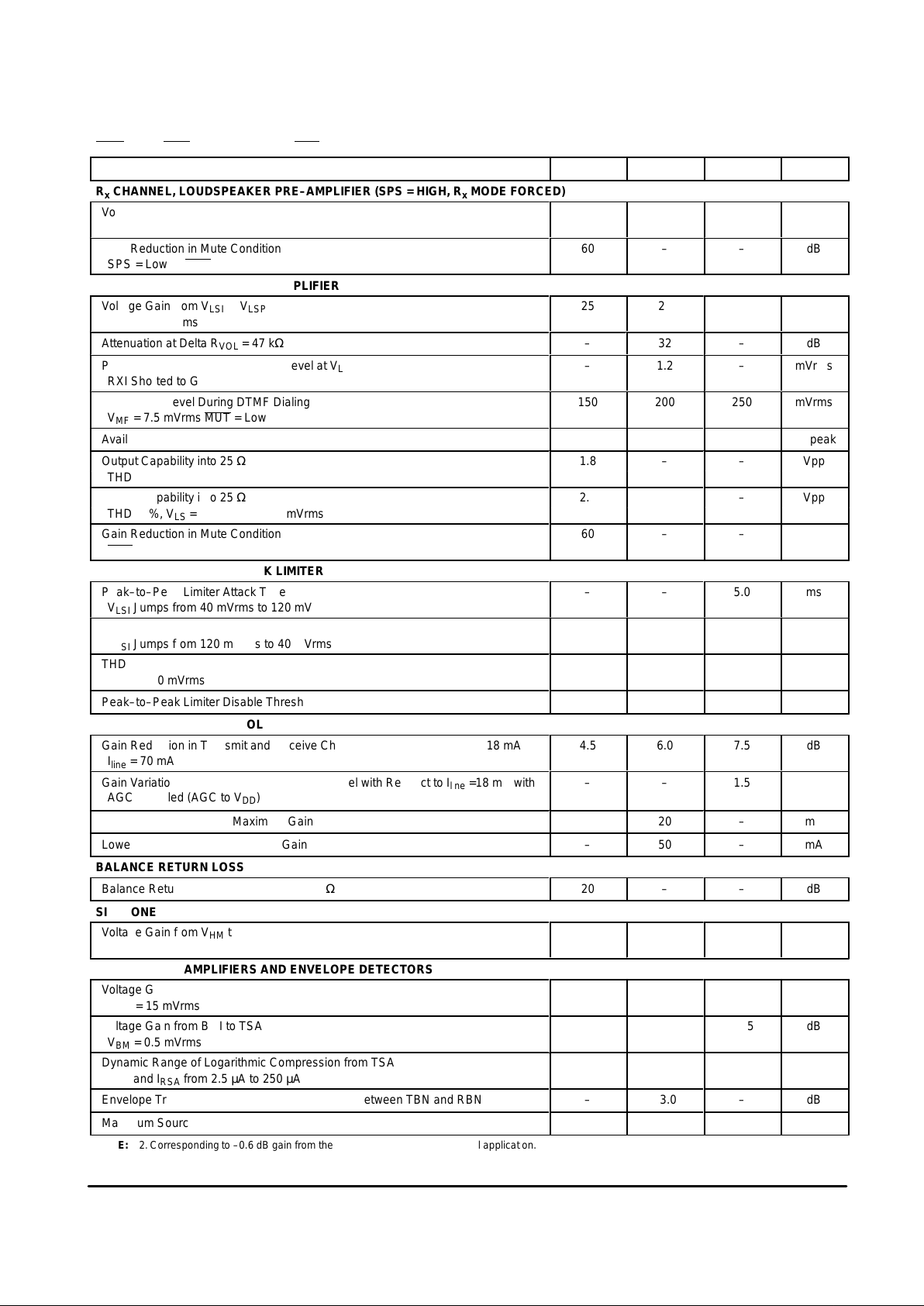
Tx CHANNEL, HANDSET MICROPHONE AMPLIFIER
Voltage Gain from VHM to V
line
46
ÁÁÁÁ
47
48
dB
VHM = 1.5 mVrms
Gain Reduction in Mute Condition
60
ÁÁÁÁ
–
–
dB
MUT = Low or PRS = Low or SPS = High
Input Impedance at HM1 and HM2
14
ÁÁÁÁ
18
22
kΩ
Common Mode Rejection Ratio
–
ÁÁÁÁ
50
–
dB
Total Harmonic Distortion at VLN
–
ÁÁÁÁ
–
2.0
%
VHM = 4.5 mVrms
Psophometrically Weighted Noise Level at V
line
–
ÁÁÁÁ
–72
–
dBmp
HM1 and HM2 Shorted with 200 Ω
Tx CHANNEL, BASE MICROPHONE AMPLIFIER (SPS = HIGH, Tx MODE FORCED)
Voltage Gain from VBM to V
line
53
ÁÁÁÁ
55.5
58
dB
VBM = 0.5 mVrms
БББББББББББББББББББ
Input Impedance at BM1 and BM2
ÁÁÁ
14
ÁÁÁÁ
ÁÁÁ18ÁÁ22ÁÁ
kΩ
БББББББББББББББББББ
Common Mode Rejection Ratio
ÁÁÁ
–
ÁÁÁÁ
ÁÁÁ50ÁÁ–ÁÁ
dB
Total Harmonic Distortion at VLN
–
ÁÁÁÁ
–
2.0
%
VBM = 1.5 mV
Psophometrically Weighted Noise Level at V
line
–
ÁÁÁÁ
–62
–
dBmp
BM1 and BM2 Shorted with 200 Ω
Gain Reduction in Mute Condition
60
–
–
dB
MUT = Low or PRS = Low or SPS = Low
Tx CHANNEL, DTMF AMPLIFIER (MUT = LOW OR PRS = LOW)
Voltage Gain from VMF to V
line
34
ÁÁÁÁ
35
36
dB
VMF = 7.5 mVrms
Input Impedance at MFI
14
ÁÁÁÁ
18
22
kΩ
Gain Reduction in Mute Condition
60
ÁÁÁÁ
–
–
dB
MUT = High or PRS = Low
Rx CHANNEL, EARPIECE AMPLIFIER
Voltage Gain from V
RXI
to V
EAR
(Note 1)
23
ÁÁÁÁ
24
25
dB
V
line
= 20 mVrms
Gain Reduction in Mute Condition
60
ÁÁÁÁ
–
–
dB
MUT = Low or SPS = Low
Input Impedance at RXI
24
ÁÁÁÁ
30
36
kΩ
Psophometrically Weighted Noise Level at V
EAR
–
ÁÁÁÁ
130
–
µVrms
RXI Shorted to Gnd via 10 µF
Confidence Level During DTMF Dialing
10
ÁÁÁÁ
15
20
mVrms
VMF = 7.5 mVrms, MUT = Low
Output Swing Capability into 150 Ω
680
ÁÁÁÁ
–
–
mVpp
THD ≤2%
Output Swing Capability into 450 Ω
1800
ÁÁÁÁ
–
–
mVpp
THD ≤2%, R
RXO
= 360 kΩ
NOTE: 1.Corresponding to –0.6 dB gain from the line to output RXO in the typical application.
MC33215
5
MOTOROLA ANALOG IC DEVICE DATA
ELECTRICAL CHARACTERISTICS (continued) (All parameters are specified at T = 25°C, I
line
= 18 mA, VLS = 2.9 V, f = 1000 Hz,
PRS
= high, MUT = high, SPS = low, LSM = high, test figure in Figure 17 with S1 in position 1, unless otherwise stated.)
Characteristic UnitMaxTypMin
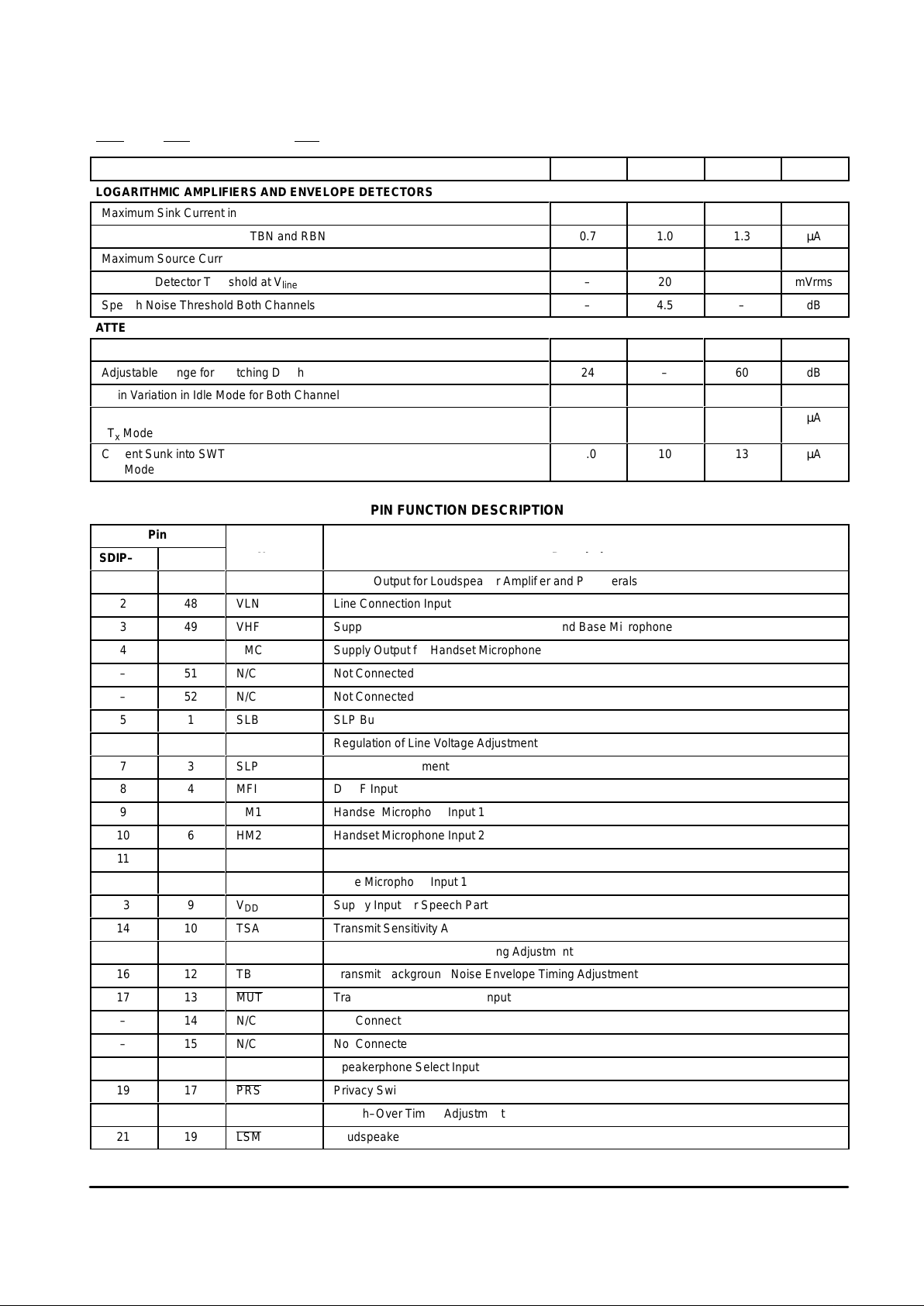
Rx CHANNEL, LOUDSPEAKER PRE–AMPLIFIER (SPS = HIGH, Rx MODE FORCED)
Voltage Gain from V
RXI
to V
RLS
(Note 2)
21
ÁÁÁÁ
24
27
dB
V
line
= 20 mVrms
Gain Reduction in Mute Condition
60
ÁÁÁÁ
–
–
dB
SPS = Low or MUT = Low
Rx CHANNEL, LOUDSPEAKER AMPLIFIER
Voltage Gain from V
LSI
to V
LSP
25
ÁÁÁÁ
26
27
dB
V
LSI
= 10 mVrms
БББББББББББББББББББ
Attenuation at Delta R
VOL
= 47 kΩ
ÁÁÁ
–
ÁÁÁÁ
ÁÁÁ32ÁÁ–ÁÁ
dB
Psophometrically Weighted Noise Level at V
LSP
–
ÁÁÁÁ
1.2
–
mVrms
RXI Shorted to Gnd via 10 µF
Confidence Level During DTMF Dialing
150
ÁÁÁÁ
200
250
mVrms
VMF = 7.5 mVrms MUT = Low
Available Peak Current from LSO
110
ÁÁÁÁ
–
–
mApeak
Output Capability into 25 Ω
1.8
–
–
Vpp
THD ≤2%, V
LSI
= 55 mVrms
Output Capability into 25 Ω
2.7
ÁÁÁÁ
–
–
Vpp
THD ≤2%, V
LS
= 5.0 V, V
LSI
= 90 mVrms
Gain Reduction in Mute Condition
60
ÁÁÁÁ
–
–
dB
LSM = Low
Rx CHANNEL PEAK–TO–PEAK LIMITER
Peak–to–Peak Limiter Attack Time
–
ÁÁÁÁ
–
5.0
ms
V
LSI
Jumps from 40 mVrms to 120 mVrms
Peak–to–Peak Limiter Release Time
–
ÁÁÁÁ
300
–
ms
V
LSI
Jumps from 120 mVrms to 40 mVrms
THD at 10 dB Overdrive
–
ÁÁÁÁ
–
7.0
%
V
LSI
= 120 mVrms
Peak–to–Peak Limiter Disable Threshold at PPL
–
ÁÁÁÁ
–
0.1
V
AUTOMATIC GAIN CONTROL
Gain Reduction in Transmit and Receive Channel with Respect to I
line
= 18 mA
4.5
ÁÁÁÁ
6.0
7.5
dB
I
line
= 70 mA
БББББББББББББББББББ
Á
Gain Variation in Transmit and Receive Channel with Respect to I
line
=18 mA with
AGC Disabled (AGC to VDD)
ÁÁÁ
Á
–
ÁÁÁÁ
ÁÁÁ
Á
–
ÁÁ
Á
1.5
ÁÁ
Á
dB
Highest Line Current for Maximum Gain
–
20
–
mA
Lowest Line Current for Minimum Gain
–
50
–
mA
BALANCE RETURN LOSS
Balance Return Loss with Respect to 600 Ω
20
–
–
dB
SIDETONE
Voltage Gain from VHM to V
EAR
–
–
28
dB
S1 in Position 2
LOGARITHMIC AMPLIFIERS AND ENVELOPE DETECTORS
Voltage Gain from RXI to RSA
18
20
22
dB
V
RXI
= 15 mVrms
Voltage Gain from BMI to TSA
17.5
18.5
19.5
dB
VBM = 0.5 mVrms
Dynamic Range of Logarithmic Compression from TSA to TSE and RSA to RSE
40
–
–
dB
I
TSA
and I
RSA
from 2.5 µA to 250 µA
Envelope Tracking Between TSE and RSE and Between TBN and RBN
–
±3.0
–
dB
Maximum Source Current from TSE or RSE
0.3
0.4
0.5
µA
NOTE: 2.Corresponding to –0.6 dB gain from the line to output RLS in the typical application.
MC33215
6
MOTOROLA ANALOG IC DEVICE DATA
ELECTRICAL CHARACTERISTICS
(continued) (All parameters are specified at T = 25°C, I
line
= 18 mA, VLS = 2.9 V, f = 1000 Hz,
PRS
= high, MUT = high, SPS = low, LSM = high, test figure in Figure 17 with S1 in position 1, unless otherwise stated.)
Characteristic UnitMaxTypMin
LOGARITHMIC AMPLIFIERS AND ENVELOPE DETECTORS
Maximum Sink Current into TSE or RSE
100
–
–
µA
Maximum Sink Current into TBN and RBN
0.7
1.0
1.3
µA
Maximum Source Current from TBN or RBN
100
–
–
µA
Dial Tone Detector Threshold at V
line
–
20
–
mVrms
Speech Noise Threshold Both Channels
–
4.5
–
dB
ATTENUATOR CONTROL
Switching Depth
46
50
54
dB
Adjustable Range for Switching Depth
24
–
60
dB
Gain Variation in Idle Mode for Both Channels
–
25
–
dB
Current Sourced from SWT
7.0
10
13
µA
Tx Mode
Current Sunk into SWT
7.0
10
13
µA
Rx Mode
PIN FUNCTION DESCRIPTION
Pin
SDIP–42 TQFP–52
Name Description
1
47
V
CC
Supply Output for Loudspeaker Amplifier and Peripherals
2
48
VLN
Line Connection Input
3
49
VHF
Supply Output for Speakerphone Section and Base Microphone
4
50
VMC
Supply Output for Handset Microphone
–
51
N/C
Not Connected
–
52
N/C
Not Connected
5
1
SLB
SLP Buffered Output
6
2
REG
Regulation of Line Voltage Adjustment
7
3
SLP
DC Slope Adjustment
8
4
MFI
DTMF Input
9
5
HM1
Handset Microphone Input 1
10
6
HM2
Handset Microphone Input 2
11
7
BM2
Base Microphone Input 2
12
8
BM1
Base Microphone Input 1
13
9
V
DD
Supply Input for Speech Part
14
10
TSA
Transmit Sensitivity Adjustment
15
11
TSE
Transmit Signal Envelope Timing Adjustment
16
12
TBN
Transmit Background Noise Envelope Timing Adjustment
17 13 MUT Transmit and Receive Mute Input
–
14
N/C
Not Connected
–
15
N/C
Not Connected
18
16
SPS
Speakerphone Select Input
19 17 PRS Privacy Switch Input
20
18
SWT
Switch–Over Timing Adjustment
21 19 LSM Loudspeaker Mute Input
 Loading...