

MOTOROLA MC33207P, MC33206DR2, MC33206DTB, MC33206DTBR2, MC33207DR2 Datasheet
SEMICONDUCTOR
TECHNICAL DATA
LOW VOLTAGE
RAIL–TO–RAIL
OPERATIONAL AMPLIFIERS
Order this document by MC33206/D
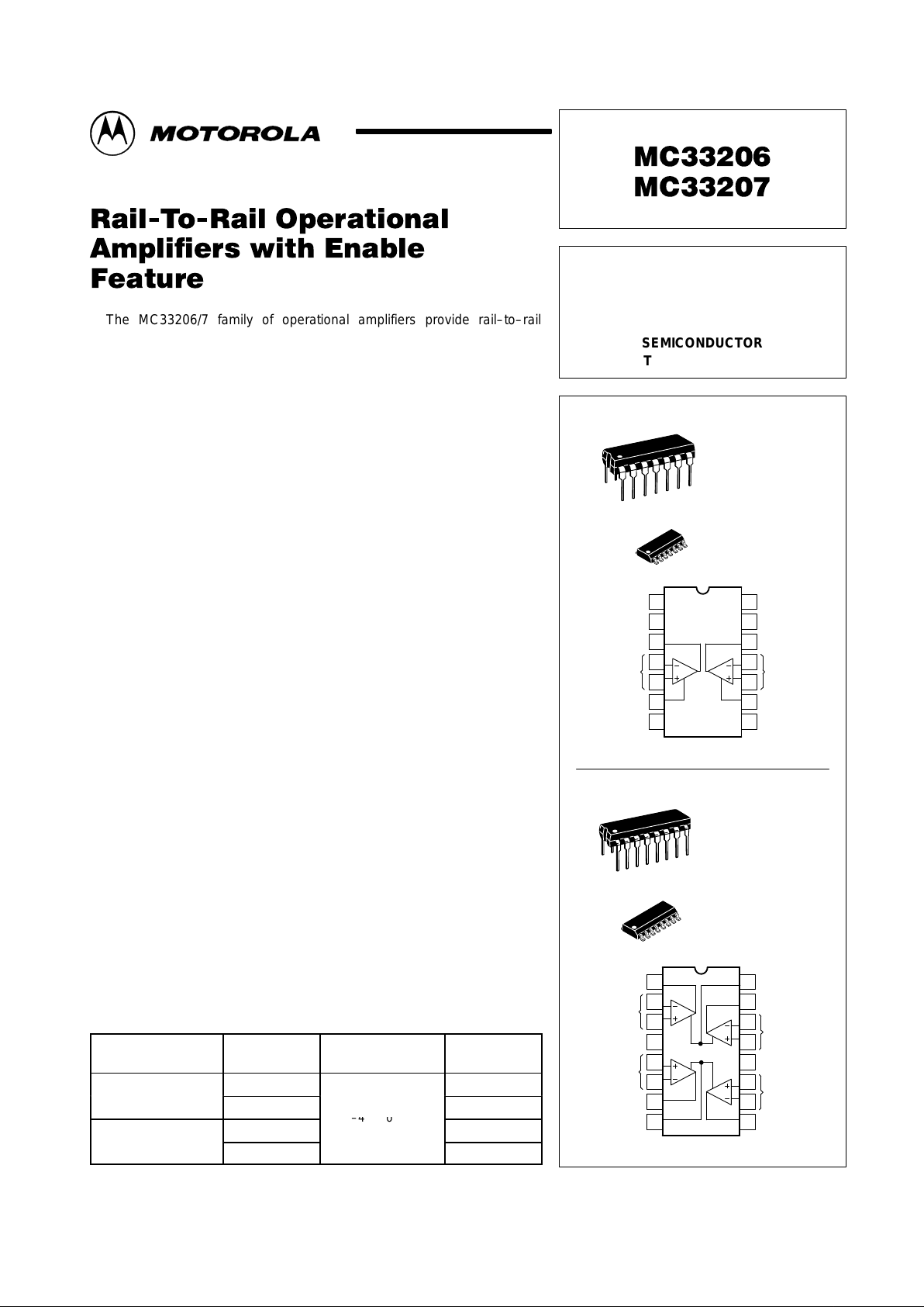
P SUFFIX
PLASTIC PACKAGE
CASE 646
14
1
D SUFFIX
PLASTIC PACKAGE
CASE 751A
(SO–14)
14
1
P SUFFIX
PLASTIC PACKAGE
CASE 648
16
1
D SUFFIX
PLASTIC PACKAGE
CASE 751B
(SO–16)
16
1
(Dual, Top View)
N.C.
Inputs 1
N.C.
12
13
14
11
3
2
1
4
105
96
V
EE
8
7
1
2
Inputs 2
N.C.
N.C.
Output 1
Enable 1
V
CC
Output 2
Enable 2
(Quad, Top View)
Output 1
Inputs 1
V
CC
Enable 1, 4
Inputs 4
1
14
15
16
13
3
2
1
4
125
116
107
Inputs 2 2
4
3
V
EE
Inputs 3
Enable 2, 3
9
8
Output 3
Output 2
Output 4
MC33207
MC33206
1
MOTOROLA ANALOG IC DEVICE DATA
The MC33206/7 family of operational amplifiers provide rail–to–rail
operation on both the input and output. The inputs can be driven as high as
200 mV beyond the supply rails without phase reversal on the outputs and
the output can swing within 50 mV of each rail. This rail–to–rail operation
enables the user to make full use of the supply voltage range available. It is
designed to work at very low supply voltages (±0.9 V) yet can operate with a
single supply of up to 12 V and ground. Output current boosting techniques
provide a high output current capability while keeping the drain current of the
amplifier to a minimum.
The MC33206/7 has an enable mode that can be controlled externally.
The typical supply current in the standby mode is <1.0 µA (V
Enable
= Gnd).
The addition of an enable function makes this amplifier an ideal choice for
power sensitive applications, battery powered equipment (ins trumentation and
monitoring), portable telecommunication, and sample–and–hold applications.
• Standby Mode (I
D
≤1.0 µA, Typ)
• Low V oltage, Single Supply Operation
(1.8 V and Ground to 12 V and Ground)
• Rail–to–Rail Input Common Mode Voltage Range
• Output Voltage Swings within 50 mV of both Rails
• No Phase Reversal on the Output for Over–Driven Input Signals
• High Output Current (I
SC
= 80 mA, Typ)
• Low Supply Current (I
D
= 0.9 mA, Typ)
• 600 Ω Output Drive Capability
• Typical Gain Bandwidth Product = 2.2 MHz
ORDERING INFORMATION
Operational
Amplifier Function
Device
Operating
Temperature Range
Package
MC33206D
SO–14
Dual
MC33206P
–
°
°
Plastic DIP
MC33207D
T
A
= –40 ° to +
105°C
SO–16
Quad
MC33207P Plastic DIP
Motorola, Inc. 1999 Rev 1
MC33206 MC33207
2
MOTOROLA ANALOG IC DEVICE DATA
MAXIMUM RATINGS
Rating Symbol Value Unit
Supply Voltage (VCC to VEE) V
S
13 V
ESD Protection Voltage at any Pin
Human Body Model
V
ESD
2,000 V
Voltage at any Device Pin V
DP
VS ± 0.5 V
Input Differential Voltage Range V
IDR
(Note 1) V
Common Mode Input Voltage Range (Note 2) V
CM
VCC + 0.5 to
VEE – 0.5
V
Output Short Circuit Duration (Note 3) t
s
(Note 3) sec
Maximum Junction Temperature T
J
+150 °C
Storage Temperature Range T
stg
–65 to +150 °C
Maximum Power Dissipation P
D
(Note 3) mW
NOTES: 1. The dif ferential input voltage of each amplifier is limited by two internal parallel back–to–back
diodes. For additional differential input voltage range, use current limiting resistors in series
with the input pins.
2.The common–mode input voltage range of each amplifier is limited by diodes connected from
the inputs to both power supply rails. Therefore, the voltage on either input must not exceed
either supply rail by more than 500 mV.
3.Power dissipation must be considered to ensure maximum junction temperature (TJ) is not
exceeded.
4.ESD data available upon request.
DC ELECTRICAL CHARACTERISTICS (V
CC
= 5.0 V , VEE = 0 V, V
Enable
= 5.0 V , TA = 25°C, unless otherwise noted.)
Characteristic Figure Symbol Min Typ Max Unit
Input Offset Voltage (VCM 0 to 0.5 V, VCM 1.0 to 5.0 V)
MC33206: TA = 25°C
MC33201: TA = –40° to +105°C
MC33207: TA = 25°C
MC33202: TA = –40° to +105°C
– V
IO
–
–
–
–
0.5
1.0
0.5
1.0
8.0
11
10
13
mV
Input Offset Voltage Temperature Coefficient (RS = 50 Ω)
TA = –40° to +105°C
– ∆VIO/∆T – 2.0 – µV/°C
Input Bias Current (VCM = 0 to 0.5 V, VCM = 1.0 to 5.0 V)
TA = 25°C
TA = –40° to +105°C
–
IIB
–
–
80
100
200
250
nA
Input Offset Current (VCM = 0 to 0.5 V, VCM = 1.0 to 5.0 V)
TA = 25°C
TA = –40° to +105°C
– IIO
–
–
5.0
10
50
100
nA
Common Mode Input Voltage Range – V
ICR
–
V
EE
VCC + 0.2
VEE – 0.2
V
CC
–
V
Large Signal Voltage Gain (VCC = 5.0 V , VEE = –5.0 V)
RL = 10 kΩ
RL = 600 Ω
– A
VOL
50
25
300
250
–
–
kV/V
Output Voltage Swing (VID = ±0.2 V)
RL = 10 kΩ
RL = 10 kΩ
RL = 600 Ω
RL = 600 Ω
–
V
OH
V
OL
V
OH
V
OL
4.85
–
4.75
–
4.95
0.05
4.85
0.15
–
0.15
–
0.25
V
Common Mode Rejection (Vin = 0 to 5.0 V) – CMR 60 90 – dB
Power Supply Rejection Ratio
VCC/VEE = 5.0 V/Gnd to 3.0 V/Gnd
– PSRR
PSR
–
66
25
92
500
–
µV/V
dB
Output Short Circuit Current (Source and Sink) – I
SC
50 80 – mA
MC33206 MC33207
3
MOTOROLA ANALOG IC DEVICE DATA
DC ELECTRICAL CHARACTERISTICS (continued) (V
CC
= 5.0 V , VEE = 0 V, V
Enable
= 5.0 V , TA = 25°C, unless otherwise noted.)
Characteristic UnitMaxTypMinSymbolFigure
Power Supply Current (VO = 2.5 V , TA = –40° to +105°C,
per Amplifier)
MC33206: V
Enable
= 5.0 Vdc
MC33206: V
Enable
= Gnd (Standby)
MC33207: V
Enable
= 5.0 Vdc
MC33207: V
Enable
= Gnd (Standby)
– I
D
–
–
–
–
0.8
0.5
1.5
0.5
1.125
6.0
2.25
6.0
mA
µA
mA
µA
Enable Input Voltage (per Amplifier)
Enabled – Amplifier “On”
Disabled – Amplifier “Off” (Standby)
– V
Enable
–
–
VEE + 1.8
VEE + 0.3
–
–
V
Enable Input Current (Note 5) (per Amplifier)
V
Enable
= 12 V
V
Enable
= 5.0 V
V
Enable
= 1.8 V
V
Enable
= Gnd
– I
Enable
–
–
–
–
2.5
2.2
0.8
0
–
–
–
–
µA
NOTE: 5. External control circuitry must provide for an initial turn–off transient of <10 µA.
AC ELECTRICAL CHARACTERISTICS (V
CC
= 5.0 V , VEE = 0 V, V
Enable
= 5.0 V , TA = 25°C, unless otherwise noted.)
Characteristic Figure Symbol Min Typ Max Unit
Slew Rate (VS = ±2.5 V , VO = –2.0 to +2.0 V ,
RL = 2.0 kΩ, AV = 1.0)
– SR 0.5 1.0 – V/µs
Gain Bandwidth Product (f = 100 kHz) – GBW – 2.2 – MHz
Phase Margin (RL = 600 Ω, CL = 0 pF) –
O
M
– 65 – Deg
Gain Margin (RL = 600 Ω, CL = 0 pF) – A
M
– 12 – dB
Channel Separation (f = 1.0 Hz to 20 kHz, AV = 100) – CS – 90 – dB
Power Bandwidth (VO = 4.0 Vpp, RL = 600 Ω, THD ≤ 1%) – BW
P
– 28 – kHz
Total Harmonic Distortion (RL = 600 Ω, VO = 1.0 Vpp, AV = 1.0)
f = 1.0 kHz
f = 10 kHz
–
THD
–
–
0.002
0.008
–
–
%
Open Loop Output Impedance
(VO = 0 V, f = 2.0 MHz, AV = 10)
– ZO – 100 – Ω
Differential Input Resistance (VCM = 0 V) – R
in
– 200 – kΩ
Differential Input Capacitance (VCM = 0 V) – C
in
– 8.0 – pF
Equivalent Input Noise Voltage (RS = 100 Ω)
f = 10 Hz
f = 1.0 kHz
– e
n
–
–
25
20
–
–
Hz
nV/
Equivalent Input Noise Current
f = 10 Hz
f = 1.0 kHz
– i
n
–
–
0.8
0.2
–
–
pA/
Hz
Time Delay for Device to Turn On – t
on
– 10 – µs
Time Delay for Device to Turn Off – t
off
– 2.0 – µs
MC33206 MC33207
4
MOTOROLA ANALOG IC DEVICE DATA
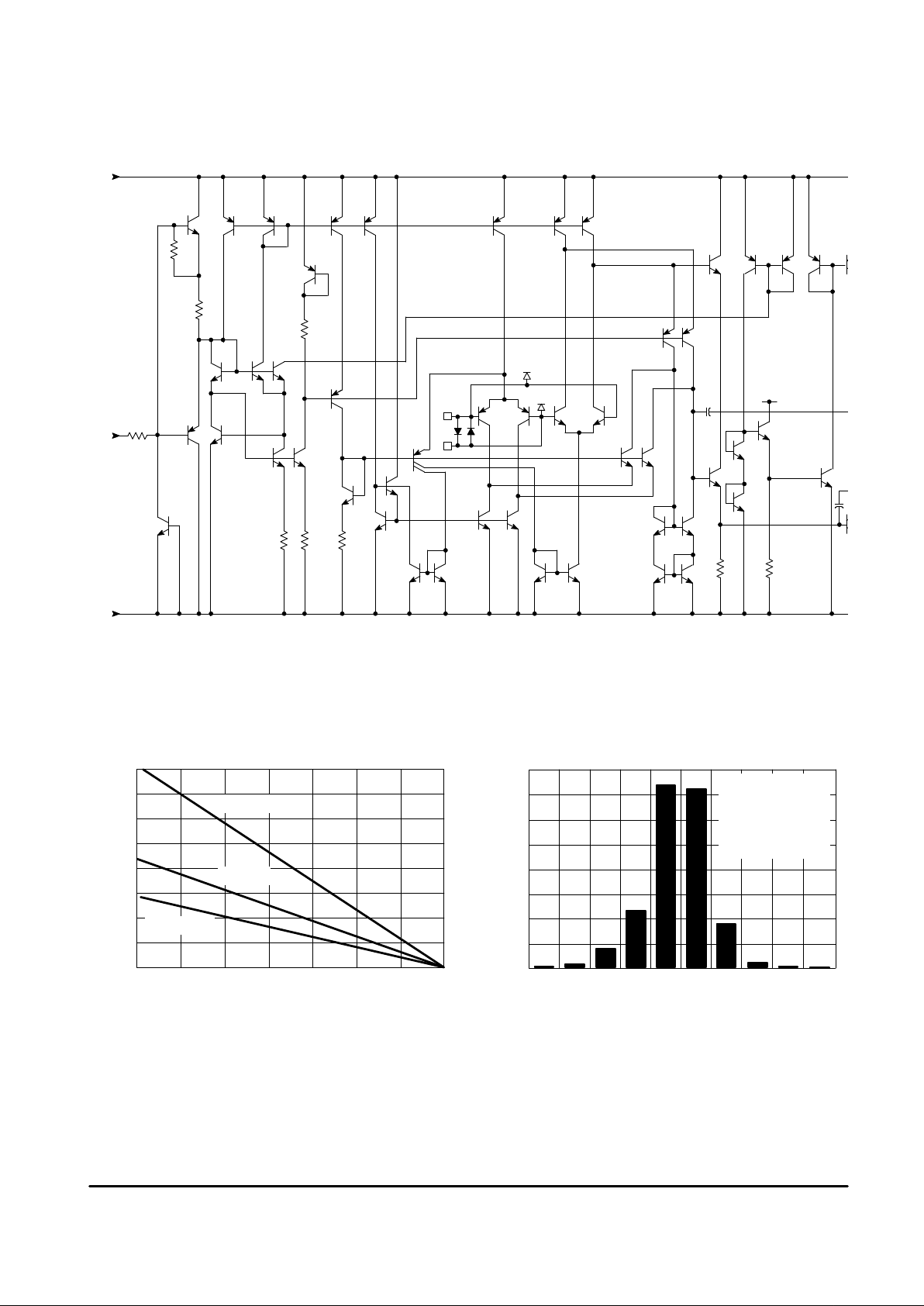
Figure 1. Circuit Schematic
(Each Amplifier)
This device contains 96 active transistors (each amplifier).
V
CC
Enable
V
EE
V
CC
V
CC
V
CC
Vin –
Vin +
Figure 2. Maximum Power Dissipation
versus Temperature
Figure 3. Input Offset Voltage Distribution
PERCENTAGE OF AMPLIFIERS (%)
40
35
VIO, INPUT OFFSET VOLTAGE (mV)
30
25
15
0
20
TA, AMBIENT TEMPERATURE (
°
C)
P
D(max)
, MAXIMUM POWER DISSIPATION (mW)
5.0
10
–10 0 4.0 8.0 10–2.0 2.0 6.0–6.0–8.0 –4.0
360 amplifiers tested
from 3 wafer lots
VCC = 5.0 V
VEE = Gnd
TA = 25
°
C
DIP Package
–60 –30
4000
3500
3000
2500
2000
1500
1000
500
0
0 30 60 90 120 150
16 Pin DIP
SO–14/SO–1
6
14 Pin DIP
 Loading...