

SEMICONDUCTOR
TECHNICAL DATA
AUTOMOTIVE WASH
WIPER TIMER
P SUFFIX
PLASTIC PACKAGE
CASE 626
8
1
18
7
6
5
2
3
4
INT
Osc2
Osc1
Out
PIN CONNECTIONS
Order this document by MC33197/D
(Top View)
D SUFFIX
PLASTIC PACKAGE
CASE 751
(SO–8)
8
1
18
7
6
5
2
3
4
Osc1
CONT
W/W
Osc2
(Top View)
CONT
Gnd
V
CC
W/W
V
CC
Gnd
Out
INT
(SO–8)
1
MOTOROLA ANALOG IC DEVICE DATA
The MC33197 is a standard wiper timer control device designed for harsh
automotive applications. The device can perform the intermittent, after wash,
and continuous wiper timer functions. It is designed to directly drive a wiper
motor relay. The MC33197 requires very few external components for full
system implementation. The intermittent control pin can be switched to
ground or V
bat
to meet a large variety of possible applications. The
intermittent timing can be fixed or adjustable via an external resistor. The
MC33197 is built using bipolar technology and parametrically specified over
the automotive ambient temperature range and 8.0 to 16 V supply voltage.
The MC33197 can operate in both front and rear wiper applications.
• Adjustable Time Interval of Less Than 500 ms to More Than 30 s
• Intermittent Control Pin Can Be Switched to Ground or V
bat
• Adjustable After Wipe Time
• Priority to Continuous Wipe
• Minimum Number of Timing Components
• Integrated Relay Driver With Free Wheeling Protection Diode
• Operating Voltage Range From 8.0 to 16 V
• For Front Wiper and Rear Wiper Window Applications
ORDERING INFORMATION
Device
Operating
Temperature Range
Package
MC33197D TA = – 40° to +105°C SO–8
MC33197P TA = – 40° to +125°C DIP–8
MAXIMUM RATINGS
Rating Symbol Value Unit
Continuous Supply Voltage (V
Pin 6
) V
CC
16 V
Storage Temperature T
stg
–55 to +150 °C
Thermal Resistance (Junction–to–Ambient) R
θJA
°C/W
DIP–8 Package 100
SO–8 Package 145
Operating Ambient Temperature Range T
A
°C
DIP–8 Package –40 to +125
SO–8 Package –40 to +105
Operating Junction Temperature Range T
J
–40 to +150 °C
Maximum Junction Temperature T
J(max)
150 °C
This document contains information on a new product. Specifications and information herein are
subject to change without notice.
Motorola, Inc. 1996
MC33197
2
MOTOROLA ANALOG IC DEVICE DATA
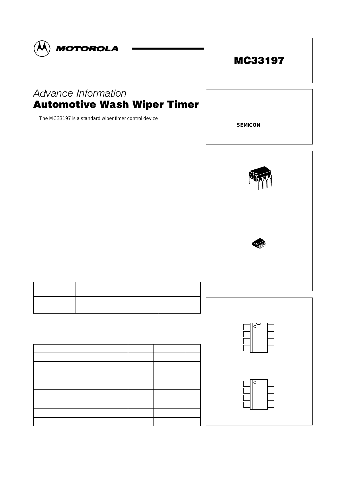
Representative Block Diagram
This device contains 390 active transistors.
R4
R5
Osc1
Osc2
INT
Logic
Ref
Ref
Ref
Input Comparator
with Hysteresis
Input
Comparator
Variable Current Sources
Out
W/W
CONT
Gnd
C2
R2
R3
R1
C1
MC33197
R1 = 220
Ω
R2 = 22 k
Ω
R3 = 1.5 to 22 k
Ω
R4 = 4.7 k
Ω
R5 = 4.7 k
Ω
C1 = 47 µF
C2 = 100 nF
Water Pump Motor
Cont Switch
Gnd
Int
V
M
Wiper
Motor
Relay
Switch
bb
V
bb
V
CC
V
bb
ELECTRICAL CHARACTERISTICS (–40°C ≤ T
A
≤ +125°C, 8.0 V ≤ VCC ≤ 16 V , unless otherwise noted. Typical values reflect approxi-
mate mean at TA = 25°C with VCC = 14 V at the time of initial device characterization.)
Characteristic Symbol Min Typ Max Unit
Functional Supply Voltage Range V
CCF
8.0 – 18 V
Operating Supply Voltage Range V
CCOP
8.0 – 16 V
Standby Supply Current (VCC = 16 V, R2 = 68 k) I
CC
– 4.0 5.2 mA
Supply Current INT Active (R3 = 2.5 k) I
CC
– 7.0 8.4 mA
Supply Current Relay “On” (R2 = 68 k) I
CC
– 7.5 11.2 mA
Supply Current INT and Relay “On” (R2 = 68 k, R3 = 2.5 k) I
CC
– 10 14.5 mA
Oscillator Variations with Supply Voltage and Temperature (excluding
external component tolerances, C2 = 100 nF polyester capacitor)
(Notes 1 & 2)
K
osc
%
10 V ≤ Vbb ≤ 16 V – 10 –
8.0 V ≤ Vbb ≤ 16 V – 15 –
Relay Resistance R
L
60 – – Ω
Output Voltage (I
out
= 200 mA) V
out
– 0.9 1.5 V
Output Clamp Voltage (I
out
= 20 mA) V
cl
19.5 – 22 V
Oscillator Period Coefficient (TA = 25°C) –
Vbb = 13 V (Note 3) t
b1
0.98 1.0 1.03
Vbb = 13 V (INT Connected to Gnd) (Note 4) t
b2g
15.1 15.5 15.9
Vbb = 13 V (INT Connected to V
bat
, R1 = 220 Ω) (Note 4) t
b2v
11.5 12.1 12.7
CONT Threshold (VCC = 13 V) V
ih
6.0 – 8.5 V
CONT Threshold (VCC = 16 V) V
ih
– VCC/2 – V
NOTES: 1. The oscillator frequency is defined by the current flowing through the external resistor R2. The voltage at the INT pin is (VCC/2 – Vbe) and hence the
current flowing through R3 is different if R3 is connected to Vbb or to Gnd because of the voltage drop across resistor R1. This voltage drop causes
the oscillator coefficient for tb2 to be different for the two cases of INT terminated to Gnd or to Vbb. Because of this, the oscillator coefficient is speci–
fied with a specific value of R1 whenever INT is connected to Vbb. If R1 is changed, the coefficient will change. Also, any extra current through the
resistor R1 other than the current used by the device will cause timing deviations in tb2 timings (as in the case where two devices are sharing a
common R1 resistor).
2. The oscillator stability with temperature is dependent on the temperature coefficients of the external components. If the capacitance value of the
external capacitor varies more than 5% over the parametric temperature range, the figures quoted for oscillator variation are not valid.
3. The tb1 duration is given by coefficient 4 x R2 x C2 (tb1 duration = tb1 x 4 x R2 x C2).
4. The tb2 duration is given by coefficient x R3 x C2 (tb2 duration = tb2 x R3 x C2).
MC33197
3
MOTOROLA ANALOG IC DEVICE DATA
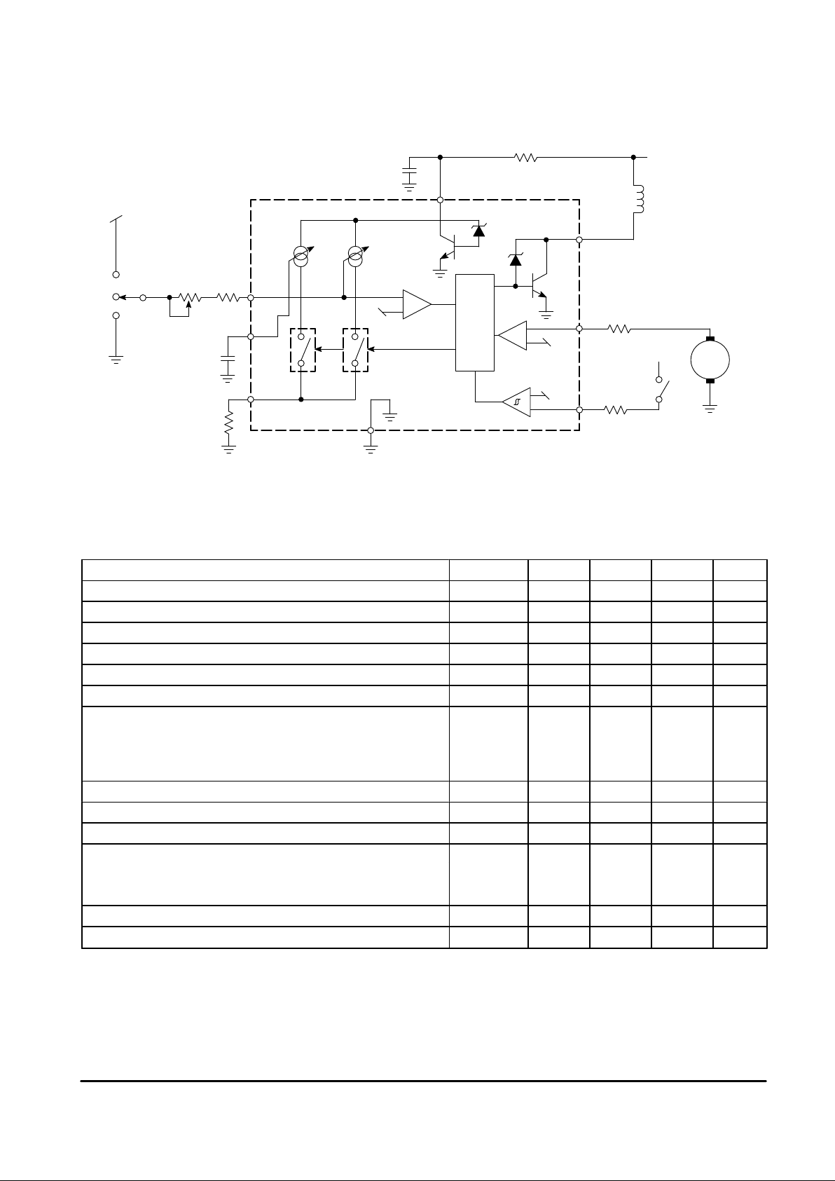
Figure 1. Intermittent Wash Wiper Typical Application
INT
Out
Gnd
V
C2
R2
R3
R1
C1
M
M
W/W
R4
Osc2 Osc1
+ Battery Line
Water
Pump
Wiper Motor
Wash Wipe
Switch
Low Speed
High Speed
MC33197
Low Speed
High Speed
Intermittent
Washer
This application shows the MC33197 with the external wirings and two speed
wiper motor. This application has the Intermittent and W ash Wiper functions.
V
bb
CC
INTRODUCTION
The MC33197 is a wiper timer control device designed for
use in harsh automotive applications. The device can
perform the intermittent, after wash, and continuous wiper
timer functions.
The MC33197 is designed to directly drive a wiper motor
relay. The MC33197 is suitable for both front and rear wiper
applications. The MC33197 connects directly to the vehicle’s
battery voltage (V
bat
) through a 220 Ω resistor used with a
47 µF de–coupling filter capacitor . The device has an internal
oscillator controlled by one of two external resistors (R2 and
R3) in addition to one external capacitor (C2), dependent on
the application function required. The values of C2 and R2
determine the tb1 time base. Tb1 is used to generate the relay
wiper activation during the INT function (T3) and the after
wash timing (T2) during the wash wipe mode. The values C2
and R3 determine the tb2 time base. The tb2 time base is
used to generate the pause or intermittent time (T4).
The intermittent wiper function can generate intermittent
timing (T4) from less than 500 ms to more than 30 seconds.
The intermittent function of the device can be activated by the
INT input connected to either ground or V
bat
. The intermittent
timing is externally adjustable by changing the value of
resistor R3.
The wash wiper timer function detects the water pump
motor’s operation. When the pump motor activation is
detected, the MC33197 turns the wiper on for the entire
duration of the pump motor’s activation. When the motor is
turned off, it generates an after wash timing (T2) to maintain
the wiping action. The W/W pin is connected to the water
pump motor through a protection resistor (R4).
The MC33197 also has a continuous function, which
activates the wiper relay whenever the CONT input is
activated. The CONT input is connected to a switch through
a protection resistor (R5). The CONT input comparator has
an input threshold of Vbb/2 with hysteresis.
The device has internal debounce circuitry, based on the
oscillator period. This provides filtering of the intermittent
(INT) and wash wipe (W/W) input signals (see T1 Debounce
Timing paragraph that follows). The device directly drives the
wiper motor relay. It internally incorporates a 20 V free
wheeling zener diode to protect the device against
overvoltage spikes produced when relay is switched off.
Intermittent Operation
Conditions:
• W/W not connected or connected to ground.
• CONT not connected or connected to ground.
• INT connected to V
bb
or to ground.
 Loading...