

Device
Operating
Temperature Range
Package
SEMICONDUCTOR
TECHNICAL DATA
AUTOMOTIVE
DIRECTION INDICATOR
ORDERING INFORMATION
MC33193D
MC33193P
TA = –40° to +125°C
SO–8
DIP–8
D SUFFIX
PLASTIC PACKAGE
CASE 751
(SO–8)
PIN CONNECTIONS
Order this document by MC33193/D
P SUFFIX
PLASTIC PACKAGE
CASE 626
8
1
8
1
15
6
7
8
2
3
4
Oscillator
Relay
V
CC
V
SS
Oscillator
Enable
Fault Detector
Starter
(Top View)
1
MOTOROLA ANALOG IC DEVICE DATA
The MC33193 is a new generation industry standard UAA1041 “Flasher”.
It has been developed for enhanced EMI sensitivity, system reliability, and
improved wiring simplification. The MC33193 is pin compatible with the
UAA1041 and UAA1041B in the standard application configuration as
shown in Figure 9, without lamp short circuit detection and using a 20 mΩ
shunt resistor. The MC33193 has a standby mode of operation requiring very
low standby supply current and can be directly connected to the vehicle’s
battery. It includes an RF filter on the Fault detection pin (Pin 7) for EMI
purposes. Fault detection thresholds are reduced relative to those of the
UAA1041, allowing a lower shunt resistance value (20 mΩ) to be used.
• Pin Compatible with the UAA1041
• Defective Lamp Detection Threshold
• RF Filter for EMI Purposes
• Load Dump Protection
• Double Battery Capability for Jump Start Protection
• Internal Free Wheeling Diode Protection
• Low Standby Current Mode
Simplified Block Diagram
1
2
3
4
8
7
6
5
SW2
SW1
Starter
24 V 33 V
Detector
Relay
Driver
Lamp Fault
Detector
Oscillator
Reference
Voltage
RF
Filter
This device contains 60 active transistors.
This document contains information on a new product. Specifications and information herein
are subject to change without notice.
Motorola, Inc. 1996 Rev 0

MC33193
2
MOTOROLA ANALOG IC DEVICE DATA
MAXIMUM RATINGS
Rating Symbol Value Unit
Pin 1 Positive Current (Continuous/Pulse) I1+ 150 to 500 mA
Pin 1 Negative Current (Continuous/Pulse) I1– –35 to –500 mA
Pin 2 Current (Continuous/Pulse) I2 ±350 to ±1900 mA
Pin 3 Current (Continuous/Pulse) I3 ±300 to ±1400 mA
Pin 8 Current (Continuous/Pulse) I8 ±25 to ±50 mA
ESD (All Pins Except Pin 4 for Negative Pulse) V
ESD
±2000 V
ESD (Pin 4 Negative Pulse) V
ESD4–
–1000 V
Junction Temperature T
J
150 °C
Operation Ambient Temperature Range T
A
–40 to +125 °C
Storage Temperature Range T
stg
–65 to +150 °C
ELECTRICAL CHARACTERISTICS (–40°C ≤ T
A
≤ +125°C, 8.0 V ≤ VCC ≤ 18 V , unless otherwise noted. Typical values
reflect approximate mean at TA = 25°C, VCC = 14 V at the time of initial device characterization.)
Characteristic
Symbol Min Typ Max Unit
Battery Voltage Range (Normal Operation) V
b
8.0 – 18 V
Overvoltage Detector Threshold (V
Pin2
– V
Pin1
) V
ih
19 20.2 22 V
Clamping Voltage (R2 = 220 Ω) V
cl
27 29.2 34 V
Output Voltage [I = –250 mA (V
Pin2
– V
Pin3
)] V
sat
– – 1.5 V
Starter Resistance (Rst = R2 + R
Lamp
) R
st
– 3.3 3.6 kΩ
Oscillator Constant (Normal Operation, TA = 25°C) K
n
1.3 1.5 1.75 X
Temperature Coefficient of K
n
TC
Kn
– 0.001 – 1/ °C
Duty Cycle (Normal Operation) – 45 50 55 %
Oscillator Constant (One 21 W Lamp Defect, TA = 25°C) K
f
0.63 0.68 0.73 X
Duty Cycle (One 21 W Lamp Defect) – 35 40 45 %
Oscillator Constant (TA = 25°C) K1
K2
0.167
0.250
0.180
0.270
0.193
0.290
–
Standby Current (Ignition “Off”) I
CC
– 2.0 100 µA
Current Consumption (Relay “Off,” Enable Pin 6 High) I
CC
mA
V
bat
= 8.0 V, R3 = 220 Ω, TA = 25°C – 1.40 –
V
bat
= 13.5 V , R3 = 220 Ω – 2.16 3.5
V
bat
= 18 V, R3 = 220 Ω, TA = 25°C – 2.64 –
Current Consumption (Relay “On”) I
CC
mA
V
bat
= 8.0 V, R3 = 220 Ω, TA = 25°C – 1.62 –
V
bat
= 13.5 V , R3 = 220 Ω – 2.06 6.0
V
bat
= 18 V, R3 = 220 Ω, TA = 25°C – 3.30 –
Defect Lamp Detector Threshold [R3 = 220 Ω, (V
Pin2
– V
Pin7
)] V
S
mV
V
bat
= 8.0 V , TA = 25°C – 43.6 –
V
bat
= 13.5 V 46.5 51.0 56
V
bat
= 18 V, TA = 25°C – 57.0 –
Temperature Coefficient of V
S
TC
Vs
– 0.3 x 10
–3
– 1/°C
MC33193
3
MOTOROLA ANALOG IC DEVICE DATA
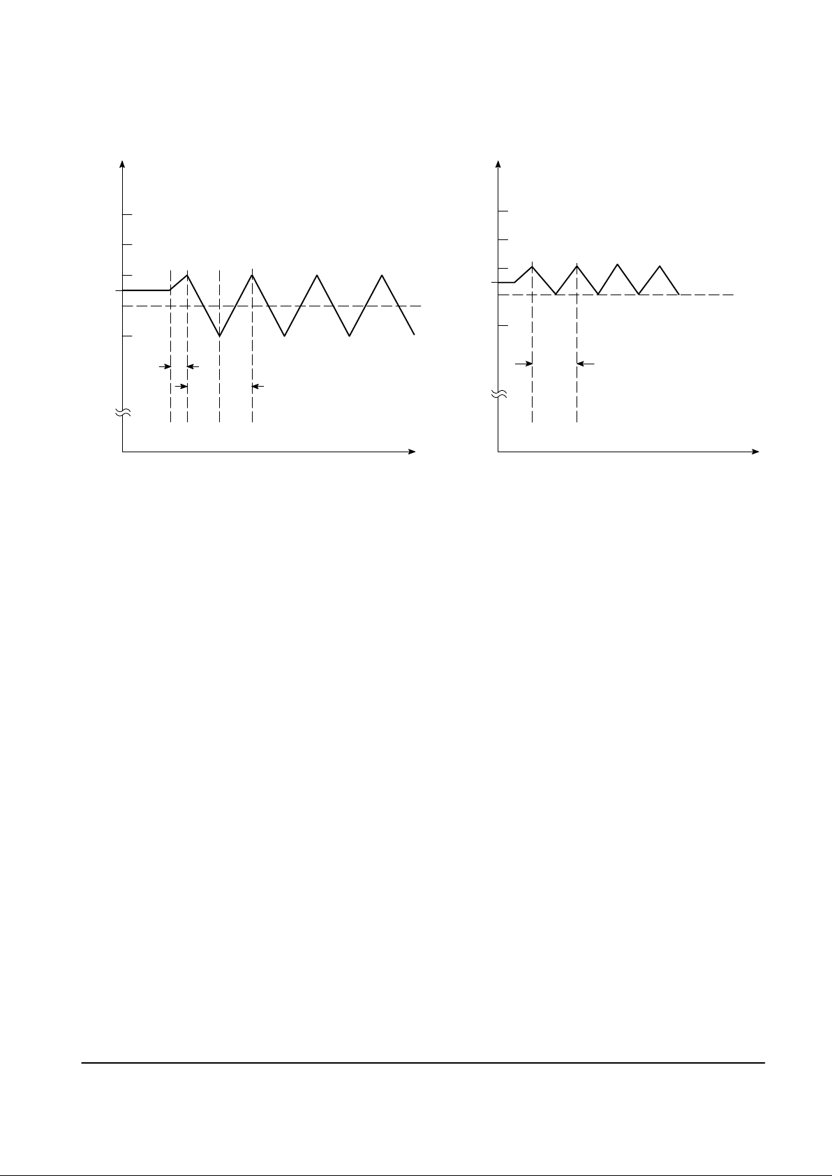
Figure 1. Normal Operation Oscillator
Timing Diagram
Figure 2. One Defective Lamp Oscillator
Timing Diagram
–4.0
–3.0
–2.0
–1.0
0
V
bat
“On” “Off”
“On” “Off”
–4.0
–3.0
–2.0
–1.0
0
V
bat
t1
t
n
t
f
Fn = 1/t
n
Ft = 1/t
f
TIME TIME
INTRODUCTION
The MC33193 is designed to drive the direction indicator
flasher relay. It is a new generation industry standard
UAA1041 “Flasher”. It consists of the following functions:
• Supply and Protections
• On–Chip Relay Driver
• Oscillator
• Starter Functions
• Lamp Fault Detector with Internal RF Filter
• Standby Mode
Supply and Protection Systems
Pin 1 is connected to ground via resistor R3 which limits
the current in the event of any high voltage transients. Pin 2
(VCC) is the positive supply and may be connected directly to
the vehicle’s battery voltage.
Overvoltage and Double Battery Protection:
When the
applied VCC to VSS voltage is greater than 22 V, the
overvoltage detector circuit turns the relay driver off. Both the
device and the lamps are protected if two 12 V batteries are
connected in series and used to jump start the vehicle.
Load Dump Overvoltage Protection:
A 29 V overvoltage
detector protects the circuits against high voltage transients
due to load dumps and other low energy spikes. The relay
driver is automatically turned on whenever the VCC to V
SS
voltage is greater than 34 V.
Overvoltage Protection, High Voltage Transients:
The
Enable and the Starter pins are protected against positive
and negative transients by internal on–chip diodes.
On–Chip Relay Driver
The device directly drives the flasher relay. The output
structure is an Emitter of an NPN transistor. It contains the
free wheeling diode circuitry necessary to protect the device
whenever the relay is switched off.
Oscillator
The device uses a sawtooth oscillator (Figure 1).
The frequency is determined by the external components
C1 and R1. In the normal operating mode, the flashing
frequency is: Fn = 1/R1*C1*Kn. With a defective (open) 21 W
lamp (Figure 2), the flashing frequency changes to: Fn =
2.2*Fn.
The typical first flash delay (the time between the moment
when the indicator switch is closed and the first lamp flash
occurs) is: t1 = K1*R1*C1
The fault detection delay is from the time relay R1 is on and
fault detection is enabled. Where a 21 W lamp opens, the
delay is expressed as: t2 = K2*R1*C1
Starter
Pin 8 is connected through a 3.3 kΩ resistor to the flashing
lamp. Pin 8 is the input to the Starter function and senses the
use of S1 by sensing ground through the lamp (Figures 9 and
10).
Lamp Fault Detector with Internal RF Filter
A Lamp defect is sensed by the lamp fault detector’s
monitoring of the voltage developed across the external
shunt resistor RS via the RF filter. The RS voltage drop is
compared to a V
bat
dependent internal reference voltage
(V
ref
) to validate the comparison over the full battery voltage
range. A detected fault causes the oscillator to change
frequency (Figure 2).
Standby Mode
When the ignition key and warning switches are open;
Enable is in a low state and the internal switches, SW1 and
SW2, are open and no current passes through the circuit. In
this condition, the device’s current consumption is zero
(ICC= 0). When ignition key and warning switches are
closed; Enable is in a high state with SW1 and SW2 being
closed and the circuit is powered on.
 Loading...