Motorola MC33192DW Datasheet

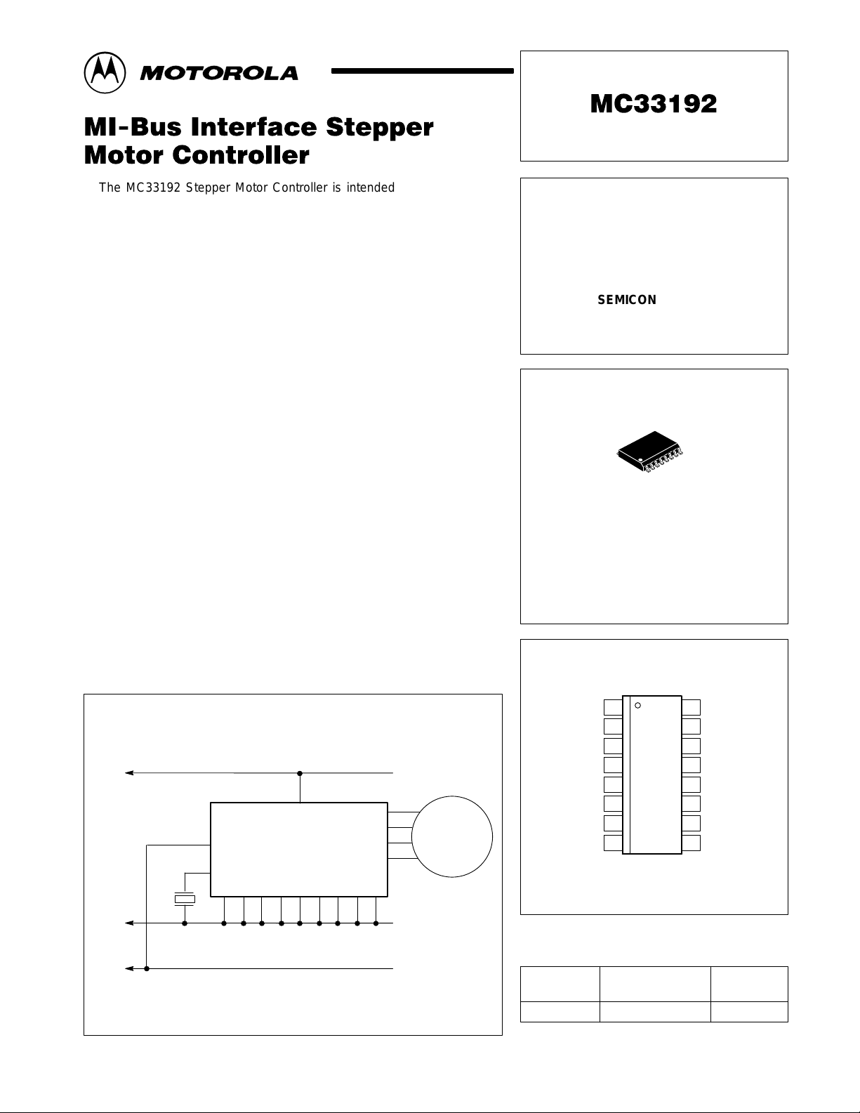
The MC33192 Stepper Motor Controller is intended to control loads in
harsh automotive environments using a serial communication bus. The
MI–Bus can provide satisfactory real time control of up to eight stepper
motors. MI–Bus technology offers a noise immune system solution for
difficult control applications involving relay drivers, motor controllers, etc.
The MC33192 stepper motor controller provides four phase signals to
drive two phase motors in either half or full step modes. When used with an
appropriate Motorola HCMOS microprocessor it provides an economical
solution for applications requiring a minimum amount of wiring and optimized
system versatility.
The MC33192 is packaged in an economical 16 pin surface mount
package and specified at an operating voltage 12 V for – 40°C ≤ TA ≤ 100°C.
• Single Wire Open Bus Capability Up to 10 Meters in Length
• Programmable Address Bus System
• Fault Detection of Half–Bridge Drivers and Motor Windings
• Ceramic Resonator For Accurate and Reliable Transmission of Data
• Sub–Multiple of Oscillator End–of–Frame Signal
• MI–Bus Signal Slew Rate Limited to 1.0 V/µs for Minimum RFI
• MI–Bus Error Diagnostics
• Non–Functioning Device Diagnotics
• Over Temperature Detection
• Address Programming Sequence Status
• Load and Double Battery (Jump Start) Protection
Order this document by MC33192/D
MI–BUS INTERFACE
STEPPER MOTOR
CONTROLLER
SEMICONDUCTOR
TECHNICAL DATA
16
1
DW SUFFIX
PLASTIC PACKAGE
CASE 751G
(SO–16L)
Simplified Application
7
V
CC
1
To
Other
Devices
MI–Bus
MI
8
Xtal
16 15 14 13 12 1 1 10 9 2
Ceramic
Resonator
This device contains 1,528 active transistors.
MC33192DW
MOTOROLA ANALOG IC DEVICE DATA
A1
A2
B1
B2
Gnd
+V
batt
3
4
5
6
Ground
From MCU
MI–Bus
Stepper
Motor
PIN CONNECTIONS
15
14
13
12
11
10
Gnd
Gnd
Gnd
Gnd
Gnd
Gnd
Gnd
Gnd
9
MI–Bus
Gnd
A1
A2
B1
B2
V
CC
Xtal
116
2
3
4
5
6
7
8
(Top View)
ORDERING INFORMATION
Operating
Device
MC33192DW TA = – 40° to +100°C
Motorola, Inc. 1996 Rev 0
Temperature Range
Package
SO–16L
1

MC33192
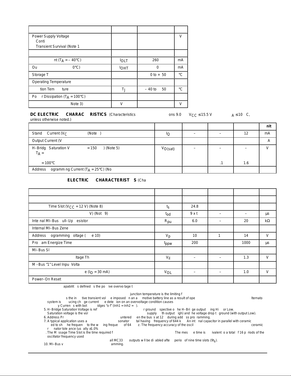
MAXIMUM RATINGS
(All voltages are with respect to ground, unless otherwise noted.)
Rating Symbol Value Limit
Power Supply Voltage
Continuous Operation V
Transient Survival (Note 1) V
Digital Input Voltage
Output Current (TA = – 40°C)
Output Current (TA = 100°C)
Storage Temperature
Operating Temperature (Note 2)
Junction Temperature
Power Dissipation (TA = 100°C)
Load Dump Transient (Note 3)
CC
V
I
OLT
I
OHT
T
stg
T
T
P
V
LD
i
A
J
D
LD
25
40
0.3 to VCC + 0.3
260
150
– 40 to +150
– 40 to +125
– 40 to +150
0.5
40
DC ELECTRICAL CHARACTERISTICS (Characteristics noted under conditions 9.0 V ≤ V
V
V
mA
mA
°C
°C
°C
W
V
≤ 15.5 V, – 40°C ≤ TA ≤ 100°C,
CC
unless otherwise noted.)
Characteristic
Standby Current (VCC = 15.5 V) (Note 4)
Output Current (VCC = 15.5 V)
H–Bridge Saturation Voltage (IO = 150 mA) (Note 5)
Symbol Min Typ Max Unit
V
O(sat)
I
Q
I
O
–
–
–
–
120
–
TA = – 40°C – 1.3 1.6
TA = 25°C – 1.2 1.6
TA = 100°C – 1.1 1.6
Address Programming Current (TA = 25°C) (Note 6)
I
pc
–
1.2
12
mA
–
–
–
mA
V
A
CONTROL LOGIC ELECTRICAL CHARACTERISTICS (Characteristics noted under conditions 9.0 V ≤ V
≤ 15.5 V, – 40°C ≤ TA ≤
CC
100°C, unless otherwise noted.)
Characteristic
Oscillator (Note 7)
Message Time Slot (VCC = 12 V) (Note 8)
Urgent Output Disable (VCC = 12 V) (Note 9)
Internal MI–Bus Pull–Up Resistor
Internal MI–Bus Zener Diode Clamp Voltage
Address Programming Voltage (Note 10)
Program Energize Time
MI–Bus Slew Rate
MI–Bus “0” Level Input Voltage Threshold
MI–Bus “1” Level Input Voltage Threshold
MI–Bus “0” Level Output Voltage (IO = 30 mA)
Power–On Reset Time (VCC ≥ 7.5 V)
NOTES: 1. Transient capability is defined as the positive overvoltage transient with 250 ms decay time constant. The detection on an overvoltage condition causes all
H–Bridges to be latched “off”.
2.Ambient temperature is given as a convience; Maximum junction temperature is the limiting factor.
3.Load Dump is the inductive transient voltage imposed on an automotive battery line as a result of opening the battery connection while the alternator
system is producing charge current. The detection on an overvoltage condition causes all H–Bridges to be latched “off”.
4.Standby Current is with both H–Bridges “off” (Inh1 = Inh2 = 0).
5.H–Bridge Saturation V oltage is referenced to the positive supply or ground respective of the H–Bridge output being High or Low.
Saturation voltage is the voltage drop from the output to the positive supply (with output High) and the voltage drop to ground (with output Low).
6.Address Programming Current is the current encountered when the bus is at 12 V during address programming.
7.A typical application uses an external ceramic resonator crystal having a frequency of 644 kHz. An internal capacitor in parallel with ceramic resonator is
used to shift the frequency to the working frequency of 640 kHz. The frequency accuracy of the oscillator is dependant on the capacitor and ceramic
resonator tolerance (usually ±1.0%).
8.The Message Time Slot is the time required for one complete device message transfer. The message time is equivalent to a total of 16 periods of the
oscillator frequency used.
9.If the MI–Bus becomes shorted to ground, all MC33192 outputs will be disabled after a period of nine time slots (9ts).
10. MI–Bus voltage required for address programming.
Symbol Min Typ Max Unit
f
cl
t
s
t
od
R
pu
V
cl
V
p
t
ppw
∆V/∆t
V
il
V
ih
V
OL
t
por
24.8
9 x t
6.0
–
10
200
1.0
–
2.4
–
–
s
640
25
–
–
18
12
1.5
–
–
–
250
–
25.2
–
20
–
14
1000
2.0
1.3
–
1.0
–
kHz
µs
µs
kΩ
V
V
µs
V/µs
V
V
V
µs
2
MOTOROLA ANALOG IC DEVICE DATA

MC33192
GENERAL DESCRIPTION
The MC33192 is a serial stepper motor controller for use in
harsh automotive applications using multiplex wiring. The
MC33192 provides all the necessary four phase drive signals
to control two phase bipolar stepper motors operated in either
half or full step modes. Multiple stepper motor controllers can
be operated on a real time basis at step frequencies up to
200 Hz using a single microcontroller (MCU). A primary
attribute of operation is the utilization of the MI–Bus message
media to provide high noise immunity communication
ensuring very high operating reliability of motor stepping.
The MC33192 is designed to drive bipolar stepper motors
having a winding resistance of 80 Ω at 20°C with a supply
voltage of 12 V. It is supplied in a SO–16L plastic package
having eight pins, on one side, connected directly to the lead
frame thus enhancing the thermal performance to allow a
power dissipation of 0.5 W at 120°C ambient temperature.
Multiple Simultaneous Motor Operation
Several motors can be controlled in a serial fashion, one
after the other, using the same software time base. The time
base determines the step frequency of the motors. A single
motor can be operated at a maximum speed of 200 Hz
pull–in with a duration of 5.0 ms per step. Three motors can
be operated simultaneously using a 68HC05B6 MCU at the
same time base (200 Hz) with about 1.7 ms per step. A
68HC11 MCU can control 4 stepper motors with adequate
program step time. The step frequency must be decreased to
control additional motors. To control eight motors
simultaneously would require the motor speed to be
decreased to 100 Hz producing about 2.0 ms time duration
per step with adequate program time.
MI–Bus General Description
The Motorola Interconnect Bus (MI–Bus) is a serial
push–pull communications protocol which efficiently
supports distributed real time control while exhibiting a high
level of noise immunity .
Under the SAE Vehicle Network categories, the MI–Bus is
a Class A bus with a data stream transfer bit rate in excess of
20 kHz and thus inaudible to the human ear. It requires a
single wire to carry the control data between the master MCU
and its slave devices. The bus can be operated at lengths up
to 15 meters.
At 20 kHz the time slot used to construct the message
(25 µs) can be handled by software using many MCUs
available on the market.
The MI–Bus is suitable for medium speed networks
requiring very low cost multiplex wiring. Aside from ground,
the MI–Bus requires only one signal wire connecting the
MCU to multiple slave MC33192 devices with individual
control.
A single MI–Bus can accomplish simultaneous automotive
system control of Air Conditioning, Head Lamp Levellers,
Window Lifts, Sensors, Intelligent Coil Drivers, etc. The
MI–Bus has been found to be cost effective in vehicle body
electronics by replacing the conventional wiring harness.
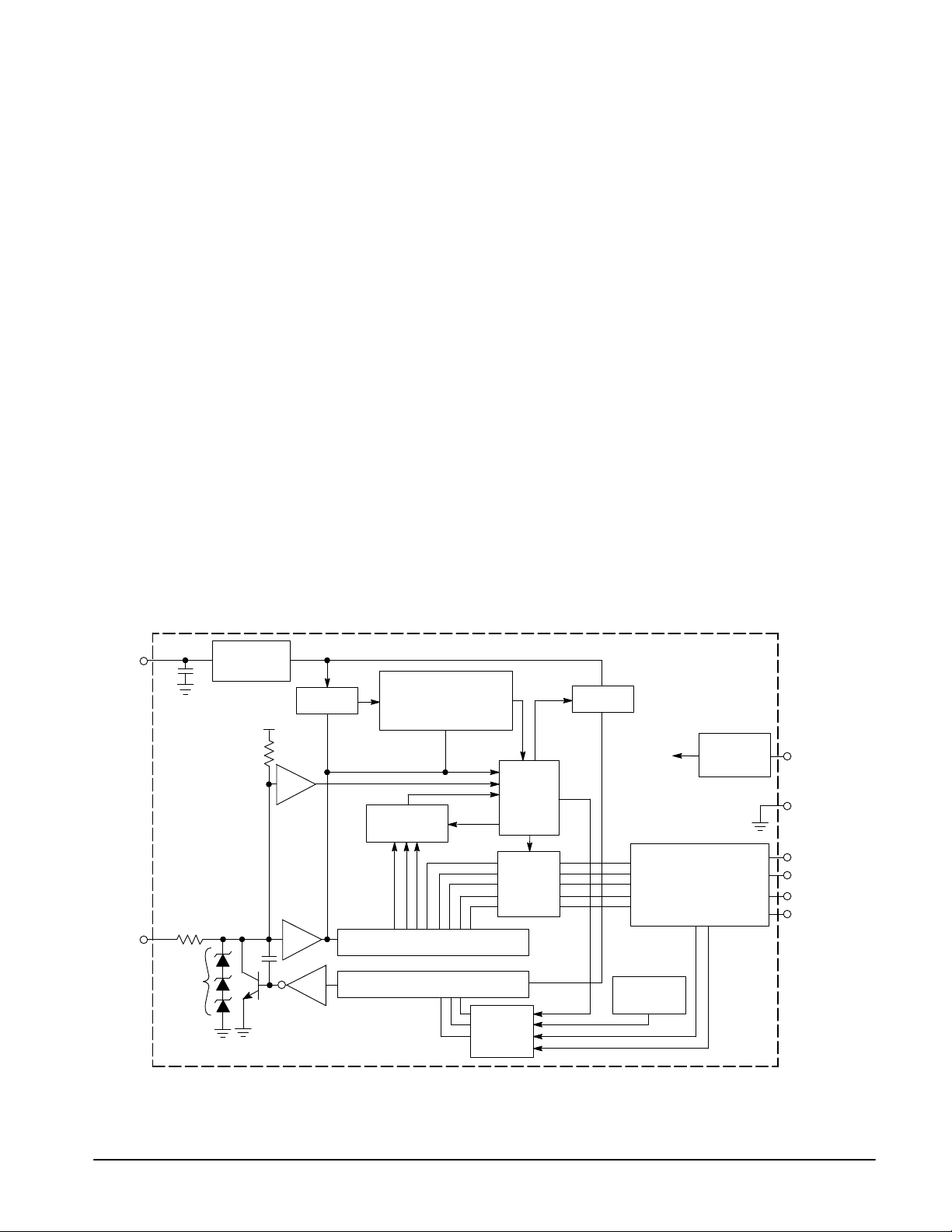
Figure 1 shows the internal block diagram of the MC33192
Stepper Motor Controller.
Xtal (8)
MI (1)
Oscillator
(640 kHz)
10 k
Programming
Level Detection
Ω
20
18 V
Figure 1. MC33192 Stepper Motor Conroller Block Diagram
5.0 V
Divider
Noise Detector
Bi–Phase
Bi–Phase Program
Programmed
Address
Serial to Parallel Register
Parallel to Serial Register
Status
Encoder
Control
Logic
Latch
Divider
20 kHz
5.0 V
Dual Bridge Driver and
Motor Diagnostics
Thermal
Shutdown
Regulator
5.0 V
+VCC (7)
Gnd (*)
A11 (3)
A12 (4)
B11 (5)
B12 (6)
NOTE: (*) Pins 2, 9, 10, 11, 12, 13, 14, 15 and 16 are common electrical and heatsink ground pins for the device.
MOTOROLA ANALOG IC DEVICE DATA
3

MC33192
ÁÁ
ББББББББ
ÁÁ
ББББББББ
ÁÁ
ББББББББ
ÁÁ
ББББББББ
ÁÁ
ББББББББ
ÁÁ
ББББББББ
ÁÁ
ББББББББ
ÁÁ
ББББББББ
ÁÁ
Á
Á
ББББББББ
Á
MI–Bus Access Method
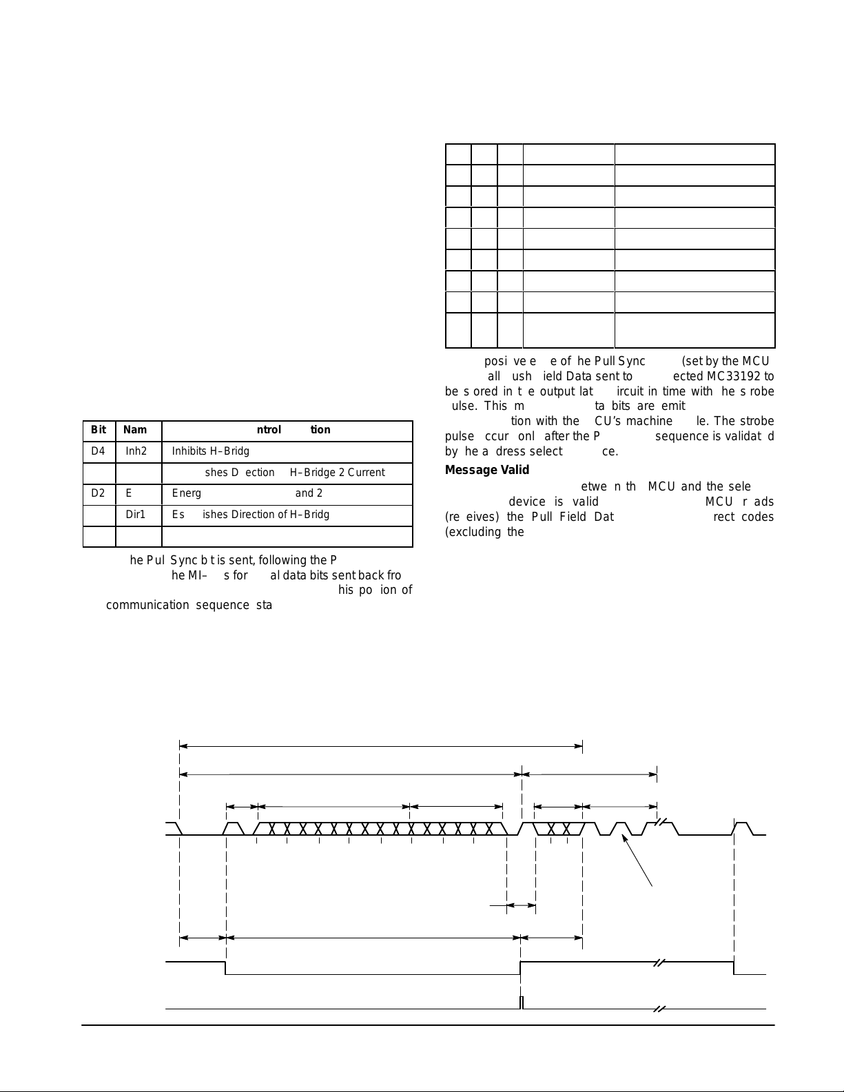
The information on the MI–Bus is sent in a fixed message
frame format (See Figure 4). The system MCU can take
control of the MI–Bus at any time with a start bit which
violates the law of Manchester Bi–Phase code by having
three consecutive Time Slots (3ts) held constantly at a Logic
“0” state.
Push–Pull Communication Sequence
Communication between the system MCU and slave
MC33192 devices always use the same message frame
organization. The MCU first sends eight serial data bits over
the MI–Bus comprised of five control bits followed by three
address bits. This communication sequence is called a “Push
Field” since it represents command information sent from the
MCU. The sequence of the five control data bits follow the
order D0, D1, D2, D3 and D4. The three address bits are sent
in sequential order A0, A1 and A2 defining a binary address
code. The condition of MI–Bus during any of the control bit
time windows defines a specific control function as shown in
Figure 2. A “Pull Sync” bit is sent at the end of the Push Field,
the positive edge of which causes all data sent to the
selected device to be latched into the output circuit.
Figure 2. Push Field Data Bits
Bit
D4
D3
D2
D1
D0
Name
Inh2
Dir2
E
Dir1
Inh1
Inhibits H–Bridge 2
Establishes Direction of H–Bridge 2 Current
Energizes Bridge Coils 1 and 2
Establishes Direction of H–Bridge 1 Current
Inhibits H–Bridge 1
Control Function
After the Pull Sync bit is sent, following the Push Field, the
MCU listens on the MI–Bus for serial data bits sent back from
the previously addressed MC33192 device. This portion of
the communication sequence starts the “Pull Field Data”
since it represents information pulled from the addressed
MC33192 and received by the MCU.
The address selected MC33192 device sends data, in
the form of status bits, back to the MCU reporting the
devices condition. At the end of the Push Field the MCU
outputs a Pull Sync bit which signals the start of the Pull
Field. In the Pull Field are three bits (S2, S1 and S0) which
report the status of the previously addressed MC33192
according to Figure 3.
Figure 3. Pull Field Status Bits
S2
S1
Á
S0
0
0
0
0
0
1
0
1
0
0
1
1
1
0
0
1
0
1
1
1
0
1
1
1
Status
Not used
Free
No Back EMF
Free
Normal/OK
Thermal
Programming
Selection failed
ÁÁÁÁ
Comments
Drivers and/or coils failed
Chip temperature > 150°C
PROM energized
Noise on MI–Bus, failed or
БББББББ
disconnected module
The positive edge of the Pull Sync pulse (set by the MCU)
causes all Push Field Data sent to the selected MC33192 to
be stored in the output latch circuit in time with the strobe
pulse. This means the data bits are emitted in real time
synchronization with the MCU’s machine cycle. The strobe
pulse occurs only after the Push Field sequence is validated
by the address selected device.
Message Validation
The communication between the MCU and the selected
MC33192 device is valid only when the MCU reads
(receives) the Pull Field Data having the correct codes
(excluding the code “1–1–1” and “0–0–0”) followed by an
End–of–Frame signal. The frequency of the End–of–Frame
signal may be a sub–multiple of the selected devices local
oscillator or related to an internal or external analog
parameter using a Voltage to Frequency Converter.
Error Detection
An error is detected when the Pull Field contains the code
“1–1–1” followed by the End–of–Frame permanently tied to a
logic “1” state (internally from 5.0 V through a pull–up
resistor). This means the communication between the MCU
and the selected device was not obtained.
MI–Bus Wire
Push/Pull Function
Strobe
4
Figure 4. MI–Bus Timing Diagram
Frame
Push Field
AddressDataPush Sync Data End–of–Frame
3t
s
234567891 1 32
“0” S1
“1”D3
S2 S0
NRZ
Bi–Phase Coded
Pull Sync
Coded
75 µs 475 µs 100 µs
Push
Strobe Pulse
MOTOROLA ANALOG IC DEVICE DATA
Pull Field
4
÷
32 = 20 kHz
Pull
Oscillator
Frequency
3t
s
StartStart “1” “0” D0 D1 D2 D4 A0 A1 A2
 Loading...