

Motorola MC14566BCP, MC14566BCL, MC14566BD Datasheet
MOTOROLA CMOS LOGIC DATA
1
MC14566B
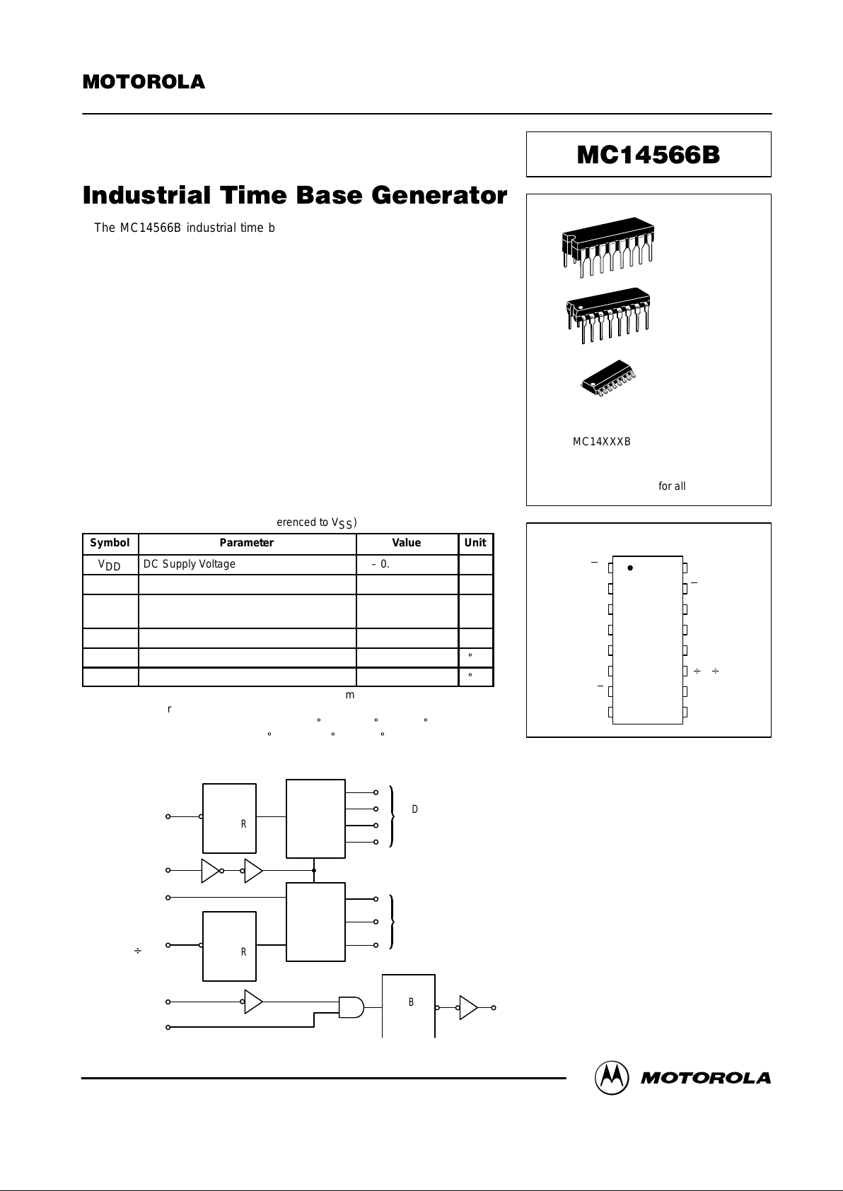
The MC14566B industrial time base generator is constructed with MOS
P–channel and N–channel enhancement mode d evices i n a single
monolithic structure. This device consists of a divide–by–10 ripple counter
and a divide–by–5 or d ivide–by–6 ripple counter to p ermit stable time
generation from a 50 or 60 Hz line. By cascading this device as divide–by–60
counters, seconds and minutes can be counted and are available in BCD
format at the circuit outputs. An internal monostable multivibrator is included
whose output can be used as a reset or clock pulse providing additional
frequency flexibility. Also a pin has been included to allow divide–by–5
counting for generating 1.0 Hz from European 50 Hz line. Pin 11 = VDD will
cause ÷ 5.
• Negative Edge Triggered Counters for Ease of Cascading
• Pulse Shapers on Counter Inputs Accept Slow Input Rise Times
• Monostable Multivibrator Positive or Negative Edge Triggered
• Diode Protection on All Inputs
• Supply Voltage Range = 3.0 Vdc to 18 Vdc
• Capable of Driving Two Low–power TTL Loads or One Low–power
Schottky TTL Load Over the Rated Temperature Range
MAXIMUM RATINGS* (Voltages Referenced to V
SS
)
Symbol
Parameter Value Unit
V
DD
DC Supply Voltage – 0.5 to + 18.0 V
Vin, V
out
Input or Output Voltage (DC or Transient) – 0.5 to VDD + 0.5 V
Iin, I
out
Input or Output Current (DC or Transient),
per Pin
± 10 mA
P
D
Power Dissipation, per Package† 500 mW
T
stg
Storage Temperature – 65 to + 150
_
C
T
L
Lead Temperature (8–Second Soldering) 260
_
C
*Maximum Ratings are those values beyond which damage to the device may occur.
†Temperature Derating:
Plastic “P and D/DW” Packages: – 7.0 mW/_C From 65_C To 125_C
Ceramic “L” Packages: – 12 mW/_C From 100_C To 125_C
BLOCK DIAGRAM
C
A
÷
10
RESET
÷5/÷
6 CONTROL
C
B
÷5/÷
6
B
A
BCD
OUT
BCD
OUT
Q
m
10
1
2
11
15
7
9
PULSE
SHAPER
PULSE
SHAPER
MONO–
STABLE
MULTI–
VIBRATOR
Q0
A
Q1
A
Q2
A
Q3
A
R
C
R
Q0
B
Q1
B
Q2
B
C
3
4
5
6
12
13
14
SEMICONDUCTOR TECHNICAL DATA
Motorola, Inc. 1995
REV 3
1/94
L SUFFIX
CERAMIC
CASE 620
ORDERING INFORMATION
MC14XXXBCP Plastic
MC14XXXBCL Ceramic
MC14XXXBD SOIC
TA = – 55° to 125°C for all packages.
P SUFFIX
PLASTIC
CASE 648
D SUFFIX
SOIC
CASE 751B
PIN ASSIGNMENT
13
14
15
16
9
10
11
125
4
3
2
1
8
7
6
Q0
B
Q1
B
Q2
B
C
B
V
DD
A
Q
m
B5/B
6
Q1
A
Q0
A
RESET
C
A
V
SS
B
Q3
A
Q2
A
MOTOROLA CMOS LOGIC DATAMC14566B
2
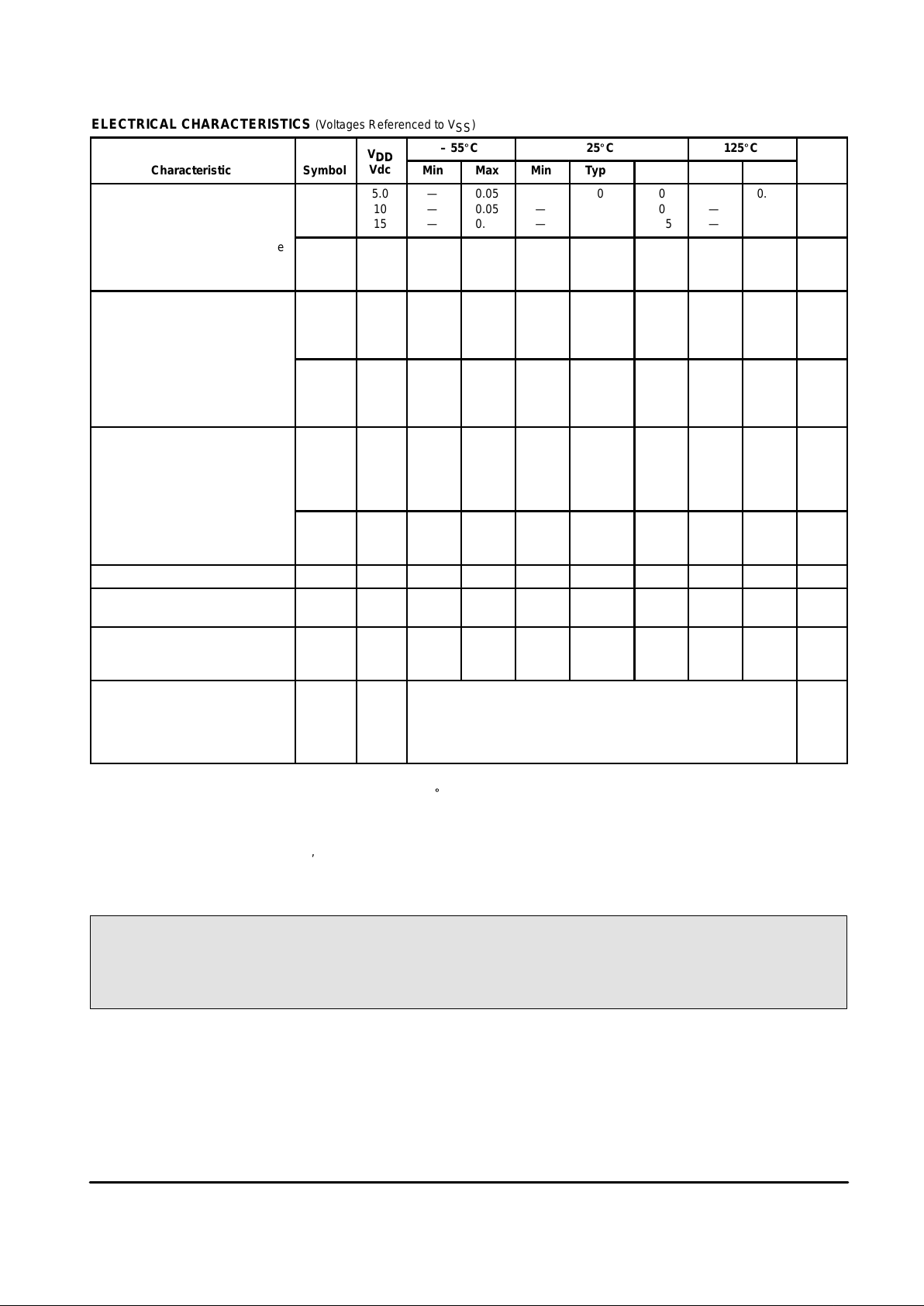
ELECTRICAL CHARACTERISTICS (Voltages Referenced to V
SS
)
V
– 55_C 25_C 125_C
Characteristic
Symbol
V
DD
Vdc
Min Max Min Typ # Max Min Max
Unit
Output Voltage “0” Level
Vin = VDD or 0
V
OL
5.0
10
15
—
—
—
0.05
0.05
0.05
—
—
—
0
0
0
0.05
0.05
0.05
—
—
—
0.05
0.05
0.05
Vdc
“1” Level
Vin = 0 or V
DD
V
OH
5.0
10
15
4.95
9.95
14.95
—
—
—
4.95
9.95
14.95
5.0
10
15
—
—
—
4.95
9.95
14.95
—
—
—
Vdc
Input Voltage “0” Level
(VO = 4.5 or 0.5 Vdc)
(VO = 9.0 or 1.0 Vdc)
(VO = 13.5 or 1.5 Vdc)
V
IL
5.0
10
15
—
—
—
1.5
3.0
4.0
—
—
—
2.25
4.50
6.75
1.5
3.0
4.0
—
—
—
1.5
3.0
4.0
Vdc
“1” Level
(VO = 0.5 or 4.5 Vdc)
(VO = 1.0 or 9.0 Vdc)
(VO = 1.5 or 13.5 Vdc)
V
IH
5.0
10
15
3.5
7.0
11
—
—
—
3.5
7.0
11
2.75
5.50
8.25
—
—
—
3.5
7.0
11
—
—
—
Vdc
Output Drive Current
(VOH = 2.5 Vdc) Source
(VOH = 4.6 Vdc)
(VOH = 9.5 Vdc)
(VOH = 13.5 Vdc)
I
OH
5.0
5.0
10
15
– 3.0
– 0.64
– 1.6
– 4.2
—
—
—
—
– 2.4
– 0.51
– 1.3
– 3.4
– 4.2
– 0.88
– 2.25
– 8.8
—
—
—
—
– 1.7
– 0.36
– 0.9
– 2.4
—
—
—
—
mAdc
(VOL = 0.4 Vdc) Sink
(VOL = 0.5 Vdc)
(VOL = 1.5 Vdc)
I
OL
5.0
10
15
0.64
1.6
4.2
—
—
—
0.51
1.3
3.4
0.88
2.25
8.8
—
—
—
0.36
0.9
2.4
—
—
—
mAdc
Input Current I
in
15 — ±0.1 — ±0.00001 ±0.1 — ±1.0 µAdc
Input Capacitance
(Vin = 0)
C
in
— — — — 5.0 7.5 — — pF
Quiescent Current
(Per Package)
I
DD
5.0
10
15
—
—
—
5.0
10
20
—
—
—
0.005
0.010
0.015
5.0
10
20
—
—
—
150
300
600
µAdc
Total Supply Current**†
(Dynamic plus Quiescent,
Per Package)
(CL = 50 pF on all outputs, all
buffers switching)
I
T
5.0
10
15
IT = (1.0 µA/kHz) f + I
DD
IT = (2.0 µA/kHz) f + I
DD
IT = (3.0 µA/kHz) f + I
DD
µAdc
#Data labelled “Typ” is not to be used for design purposes but is intended as an indication of the IC’s potential performance.
**The formulas given are for the typical characteristics only at 25_C.
†To calculate total supply current at loads other than 50 pF:
IT(CL) = IT(50 pF) + (CL – 50) Vfk
where: IT is in µA (per package), CL in pF, V = (VDD – VSS) in volts, f in kHz is input frequency, and k = 0.001.
This device contains protection circuitry to guard against damage due to high static voltages or electric fields. However,
precautions must be taken to avoid applications of any voltage higher than maximum rated voltages to this high-impedance
circuit. For proper operation, Vin and V
out
should be constrained to the range VSS ≤ (Vin or V
out
) ≤ VDD.
Unused inputs must always be tied to an appropriate logic voltage level (e.g., either VSS or VDD). Unused outputs must
be left open.
MOTOROLA CMOS LOGIC DATA
3
MC14566B
SWITCHING CHARACTERISTICS* (C
L
= 50 pF, TA = 25_C)
Characteristic
Symbol V
DD
Min Typ # Max Unit
Output Rise and Fall Time
t
TLH
, t
THL
= (1.5 ns/pF) CL + 25 ns
t
TLH
, t
THL
= (0.75 ns/pF) CL + 12.5 ns
t
TLH
, t
THL
= (0.55 ns/pF) CL + 9.5 ns
t
TLH
,
t
THL
5.0
10
15
—
—
—
100
50
40
200
100
80
ns
Propagation Delay Time, Clock to Q3
A
t
PLH
, t
PHL
= (1.7 ns/pF) CL + 1365 ns
t
PLH
, t
PHL
= (0.66 ns/pF) CL + 497 ns
t
PLH
, t
PHL
= (0.5 ns/pF) CL + 295 ns
t
PLH
,
t
PHL
5.0
10
15
—
—
1450
530
320
4500
1500
1000
ns
Propagation Delay Time, Reset to Q3
A
t
PHL
= (1.7 ns/pF) CL + 845 ns
t
PHL
= (0.66 ns/pF) CL + 282 ns
t
PHL
= (0.5 ns/pF) CL + 185 ns
t
PHL
5.0
10
15
—
—
—
930
315
210
3000
1000
750
ns
Clock Pulse Width t
WH(cl)
5.0
10
15
1200
400
270
400
125
90
—
—
—
ns
Reset Pulse Width t
WH(R)
5.0
10
15
1200
400
270
400
125
90
—
—
—
ns
Clock Pulse Frequency f
cl
5.0
10
15
—
—
—
1.0
2.5
4.2
0.3
1.0
1.5
MHz
Clock Pulse Rise and Fall Time t
TLH
,
t
THL
5.0
10
15
No Limit
—
Monostable Multivibrator Pulse Width
t
WH(Qm)
5.0
10
15
1200
400
300
2800
900
600
—
—
—
ns
*The formulas given are for the typical characteristics only at 25_C.
#Data labelled “Typ” is not to be used for design purposes but is intended as an indication of the IC’s potential performance.
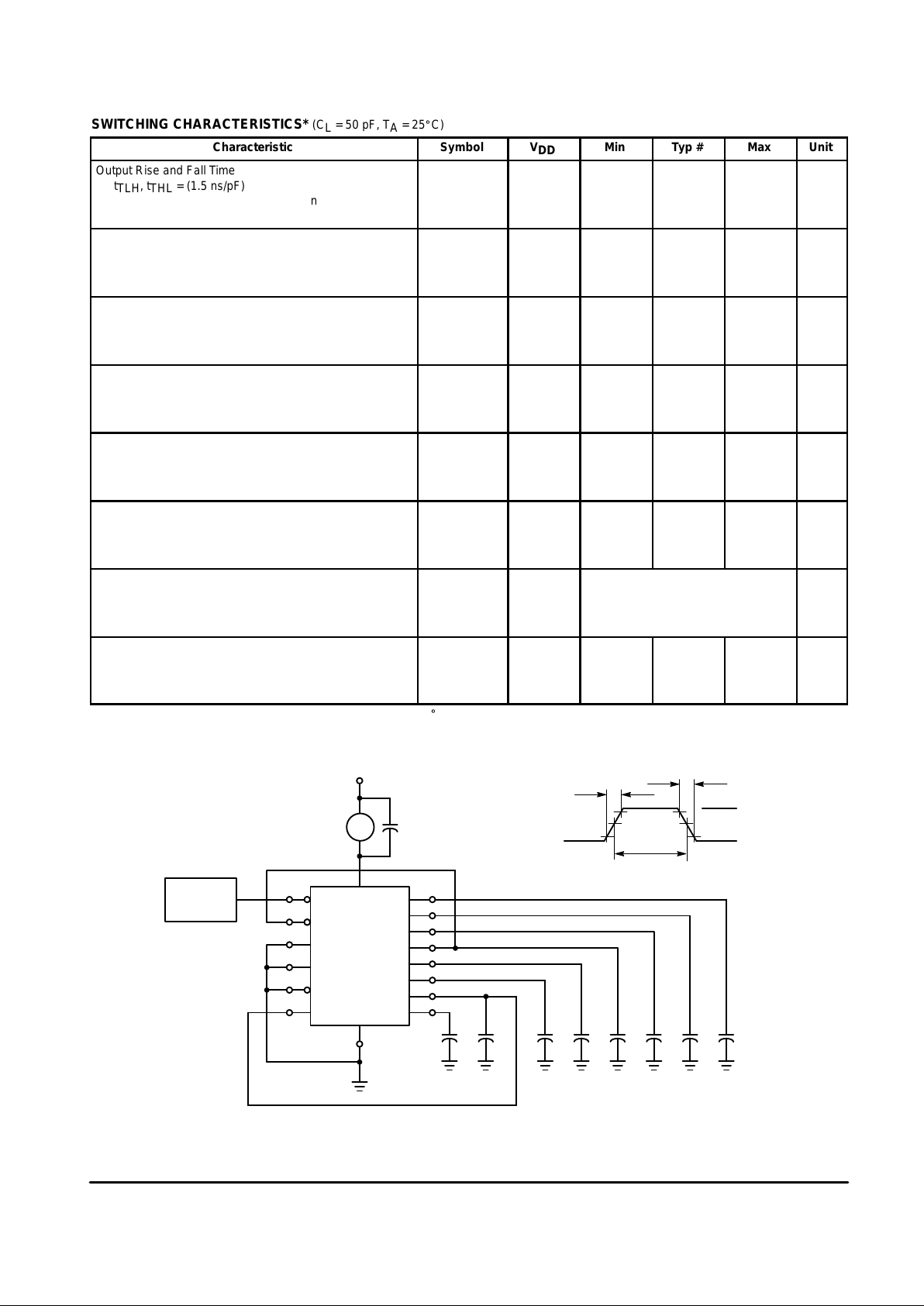
Figure 1. Power Dissipation Test Circuit and Waveform
PULSE
GENERATOR
V
in
V
DD
I
D
500
µ
F
C
A
C
B
RESET
÷5/÷
6
B
A
CONTROL
Q0
A
Q1
A
Q2
A
Q3
A
Q0
B
Q1
B
Q2
B
Q
m
V
SS
C
L
C
L
C
L
C
L
C
L
C
L
C
L
C
L
20 ns
20 ns
V
DD
V
SS
90%
50%
10%
V
in
VARIABLE
WIDTH
 Loading...