

Motorola MC14560BCL, MC14560BCP, MC14560BD Datasheet
MOTOROLA CMOS LOGIC DATA
1
MC14560B
The MC14560B adds two 4–bit numbers in NBCD (natural binary coded
decimal) format, resulting in sum and carry outputs in NBCD code.
This device can also subtract when one set of inputs is complemented with
a 9’s Complementer (MC14561B).
All i nputs a nd outputs a re active high. T he carry input for the l east
significant digit is connected to VSS for no carry in.
• Diode Protection on All Inputs
• Supply Voltage Range = 3.0 Vdc to 18 Vdc
• Capable of Driving Two Low–power TTL Loads or One Low–power
Schottky TTL Load Over the Rated Temperature Range
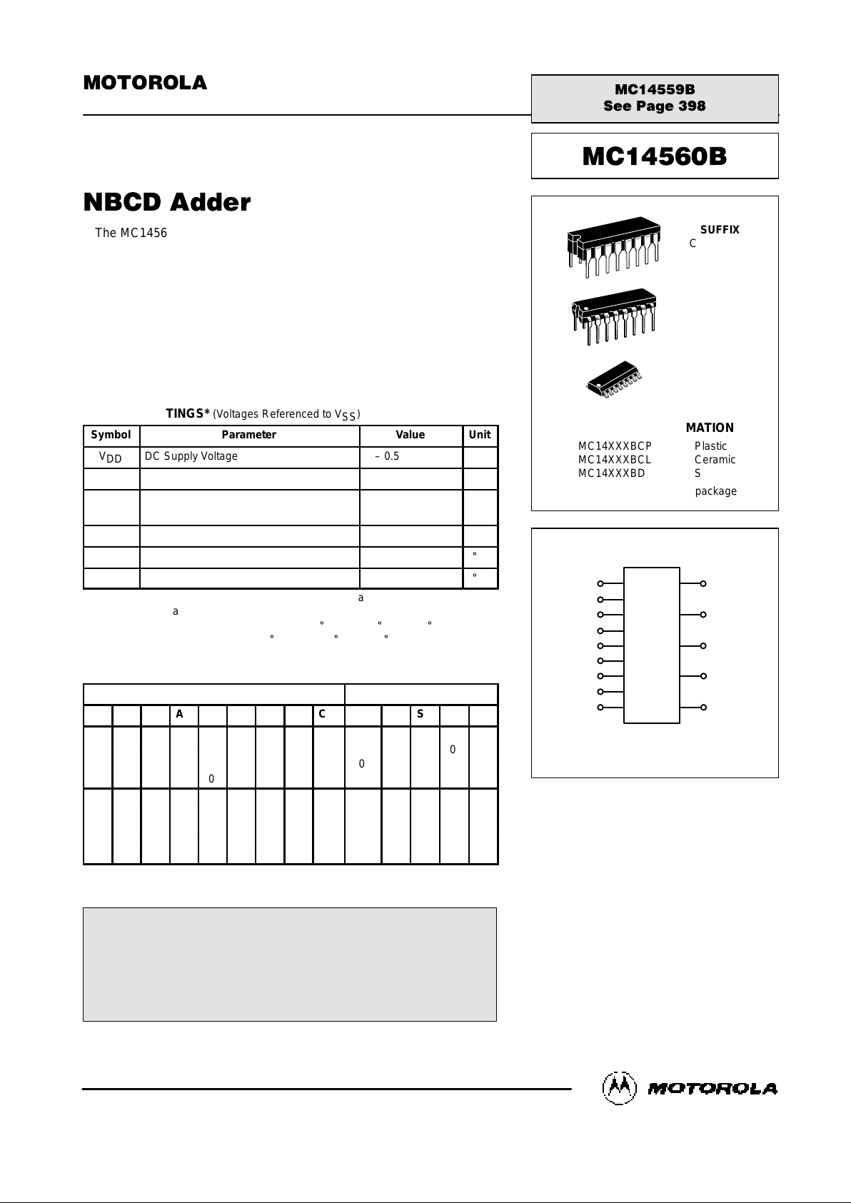
MAXIMUM RATINGS* (Voltages Referenced to V
SS
)
Symbol
Parameter Value Unit
V
DD
DC Supply Voltage – 0.5 to + 18.0 V
Vin, V
out
Input or Output Voltage (DC or Transient) – 0.5 to VDD + 0.5 V
Iin, I
out
Input or Output Current (DC or Transient),
per Pin
± 10 mA
P
D
Power Dissipation, per Package† 500 mW
T
stg
Storage Temperature – 65 to + 150
_
C
T
L
Lead Temperature (8–Second Soldering) 260
_
C
*Maximum Ratings are those values beyond which damage to the device may occur.
†Temperature Derating:
Plastic “P and D/DW” Packages: – 7.0 mW/_C From 65_C To 125_C
Ceramic “L” Packages: – 12 mW/_C From 100_C To 125_C
TRUTH TABLE*
Input Output
A4 A3 A2 A1 B4 B3 B2 B1 CinC
out
S4 S3 S2 S1
0 0 0 0 0 0 0 0 0 0 0 0 0 0
0 0 0 0 0 0 0 0 1 0 0 0 0 1
0 1 0 0 0 0 1 1 0 0 0 1 1 1
0 1 0 0 0 0 1 1 1 0 1 0 0 0
0 1 1 1 0 1 0 0 0 1 0 0 0 1
0 1 1 1 0 1 0 0 1 1 0 0 1 0
1 0 0 0 0 1 0 1 0 1 0 0 1 1
0 1 1 0 1 0 0 0 0 1 0 1 0 0
1 0 0 1 1 0 0 1 1 1 1 0 0 1
*Partial truth table to show logic operation for representative input values.
This device contains protection circuitry to guard against damage
due to high static voltages or electric fields. However, precautions must
be taken to avoid applications of any voltage higher than maximum rated
voltages to this high-impedance circuit. For proper operation, Vin and
V
out
should be constrained to the range VSS ≤ (Vin or V
out
) ≤ VDD.
Unused inputs must always be tied to an appropriate logic voltage
level (e.g., either VSS or VDD). Unused outputs must be left open.
SEMICONDUCTOR TECHNICAL DATA
Motorola, Inc. 1995
REV 3
1/94
Motorola, Inc. 1994
REV 0
1/94
BLOCK DIAGRAM
L SUFFIX
CERAMIC
CASE 620
ORDERING INFORMATION
MC14XXXBCP Plastic
MC14XXXBCL Ceramic
MC14XXXBD SOIC
TA = – 55° to 125°C for all packages.
P SUFFIX
PLASTIC
CASE 648
D SUFFIX
SOIC
CASE 751B
7 13
15
14
1
2
3
4
5
6
12
11
10
9
C
in
A1
B1
A2
B2
A3
B3
A4
B4
S1
S2
S3
S4
C
out
VDD = PIN 16
VSS = PIN 8
MOTOROLA CMOS LOGIC DATAMC14560B
2
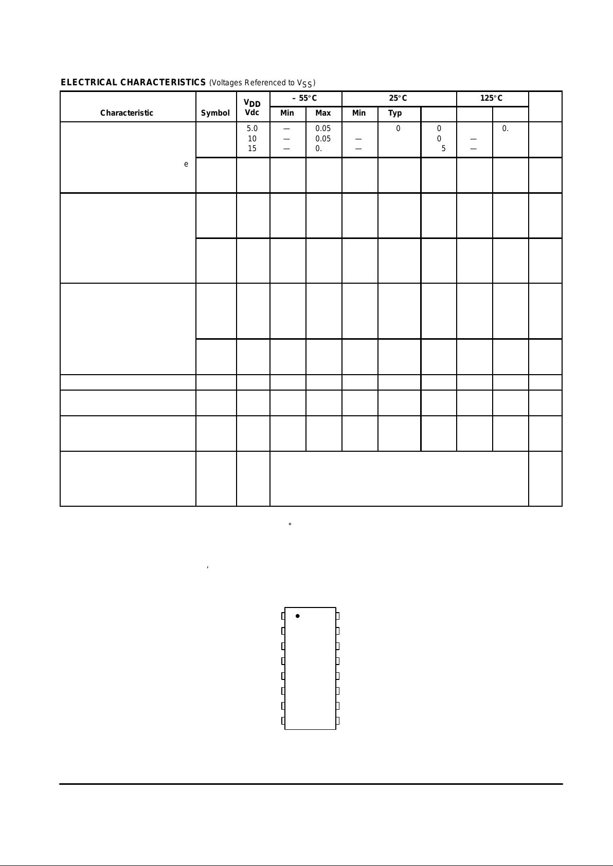
ELECTRICAL CHARACTERISTICS (Voltages Referenced to V
SS
)
V
– 55_C 25_C 125_C
Characteristic
Symbol
V
DD
Vdc
Min Max Min Typ # Max Min Max
Unit
Output Voltage “0” Level
Vin = VDD or 0
V
OL
5.0
10
15
—
—
—
0.05
0.05
0.05
—
—
—
0
0
0
0.05
0.05
0.05
—
—
—
0.05
0.05
0.05
Vdc
“1” Level
Vin = 0 or V
DD
V
OH
5.0
10
15
4.95
9.95
14.95
—
—
—
4.95
9.95
14.95
5.0
10
15
—
—
—
4.95
9.95
14.95
—
—
—
Vdc
Input Voltage “0” Level
(VO = 4.5 or 0.5 Vdc)
(VO = 9.0 or 1.0 Vdc)
(VO = 13.5 or 1.5 Vdc)
V
IL
5.0
10
15
—
—
—
1.5
3.0
4.0
—
—
—
2.25
4.50
6.75
1.5
3.0
4.0
—
—
—
1.5
3.0
4.0
Vdc
“1” Level
(VO = 0.5 or 4.5 Vdc)
(VO = 1.0 or 9.0 Vdc)
(VO = 1.5 or 13.5 Vdc)
V
IH
5.0
10
15
3.5
7.0
11
—
—
—
3.5
7.0
11
2.75
5.50
8.25
—
—
—
3.5
7.0
11
—
—
—
Vdc
Output Drive Current
(VOH = 2.5 Vdc) Source
(VOH = 4.6 Vdc)
(VOH = 9.5 Vdc)
(VOH = 13.5 Vdc)
I
OH
5.0
5.0
10
15
– 3.0
– 0.64
– 1.6
– 4.2
—
—
—
—
– 2.4
– 0.51
– 1.3
– 3.4
– 4.2
– 0.88
– 2.25
– 8.8
—
—
—
—
– 1.7
– 0.36
– 0.9
– 2.4
—
—
—
—
mAdc
(VOL = 0.4 Vdc) Sink
(VOL = 0.5 Vdc)
(VOL = 1.5 Vdc)
I
OL
5.0
10
15
0.64
1.6
4.2
—
—
—
0.51
1.3
3.4
0.88
2.25
8.8
—
—
—
0.36
0.9
2.4
—
—
—
mAdc
Input Current I
in
15 — ±0.1 — ±0.00001 ±0.1 — ±1.0 µAdc
Input Capacitance
(Vin = 0)
C
in
— — — — 5.0 7.5 — — pF
Quiescent Current
(Per Package)
I
DD
5.0
10
15
—
—
—
5.0
10
20
—
—
—
0.005
0.010
0.015
5.0
10
20
—
—
—
150
300
600
µAdc
Total Supply Current**†
(Dynamic plus Quiescent,
Per Package)
(CL = 50 pF on all outputs, all
buffers switching)
I
T
5.0
10
15
IT = (1.68 µA/kHz) f + I
DD
IT = (3.35 µA/kHz) f + I
DD
IT = (5.03 µA/kHz) f + I
DD
µAdc
#Data labelled “Typ” is not to be used for design purposes but is intended as an indication of the IC’s potential performance.
**The formulas given are for the typical characteristics only at 25_C.
†To calculate total supply current at loads other than 50 pF:
IT(CL) = IT(50 pF) + (CL – 50) Vfk
where: IT is in µA (per package), CL in pF, V = (VDD – VSS) in volts, f in kHz is input frequency, and k = 0.005.
PIN ASSIGNMENT
13
14
15
16
9
10
11
125
4
3
2
1
8
7
6
S2
S1
B1
A1
V
DD
C
out
S4
S3
B3
A3
B2
A2
V
SS
C
in
B4
A4
MOTOROLA CMOS LOGIC DATA
3
MC14560B
SWITCHING CHARACTERISTICS* (C
L
= 50 pF, TA = 25_C)
Characteristic
Symbol V
DD
Min Typ # Max Unit
Output Rise and Fall Time
t
TLH
, t
THL
= (1.5 ns/pF) CL + 25 ns
t
TLH
, t
THL
= (0.75 ns/pF) CL + 12.5 ns
t
TLH
, t
THL
= (0.55 ns/pF) CL + 9.5 ns
t
TLH
, t
THL
5.0
10
15
—
—
—
100
50
40
200
100
80
ns
Propagation Delay Time
A or B to S
t
PLH
, t
PHL
= (1.7 ns/pF) CL + 665 ns
t
PLH
, t
PHL
= (0.66 ns/pF) CL + 297 ns
t
PLH
, t
PHL
= (0.5 ns/pF) CL + 195 ns
t
PLH
, t
PHL
5.0
10
15
—
—
—
750
330
220
2100
900
675
ns
A or B to C
out
t
PLH
, t
PHL
= (1.7 ns/pF) CL + 565 ns
t
PLH
, t
PHL
= (0.66 ns/pF) CL + 197 ns
t
PLH
, t
PHL
= (0.5 ns/pF) CL + 145 ns
5.0
10
15
—
—
—
650
230
170
1800
600
450
ns
Cin to C
out
t
PLH
, t
PHL
= (1.7 ns/pF) CL + 465 ns
t
PLH
, t
PHL
= (0.66 ns/pF) CL + 187 ns
t
PLH
, t
PHL
= (0.5 ns/pF) CL + 135 ns
5.0
10
15
—
—
—
550
220
160
1500
600
450
ns
Turn–Off Delay Time
Cin to S
t
PLH
= (1.7 ns/pF) CL + 715 ns
t
PLH
= (0.66 ns/pF) CL + 197 ns
t
PLH
= (0.5 ns/pF) CL + 215 ns
t
PLH
5.0
10
15
—
—
—
800
350
240
2250
975
750
ns
Turn–On Delay Time
Cin to S
t
PHL
= (1.7 ns/pF) CL + 565 ns
t
PHL
= (0.66 ns/pF) CL + 197 ns
t
PHL
= (0.5 ns/pF) CL + 145 ns
t
PHL
5.0
10
15
—
—
—
650
230
170
1800
600
450
ns
*The formulas given are for the typical characteristics only at 25_C.
#Data labelled “Typ” is not to be used for design purposes but is intended as an indication of the IC’s potential performance.
Figure 1. Power Dissipation Waveforms
Duty Cycle = 50%
All outputs connected to respective CL loads
f = System clock frequency
Figure 2. Switching Time Waveforms
ALL INPUTS
ANY OUTPUT
20 ns
t
PLH
20 ns
V
DD
V
SS
V
OH
V
OL
90%
50%
10%
2f
1
t
PHL
V
DD
V
SS
V
OH
V
OL
20 ns20 ns
90%
50%
10%
90%
50%
10%
t
TLH
t
THL
ANY INPUT
ANY OUTPUT
MOTOROLA CMOS LOGIC DATAMC14560B
4
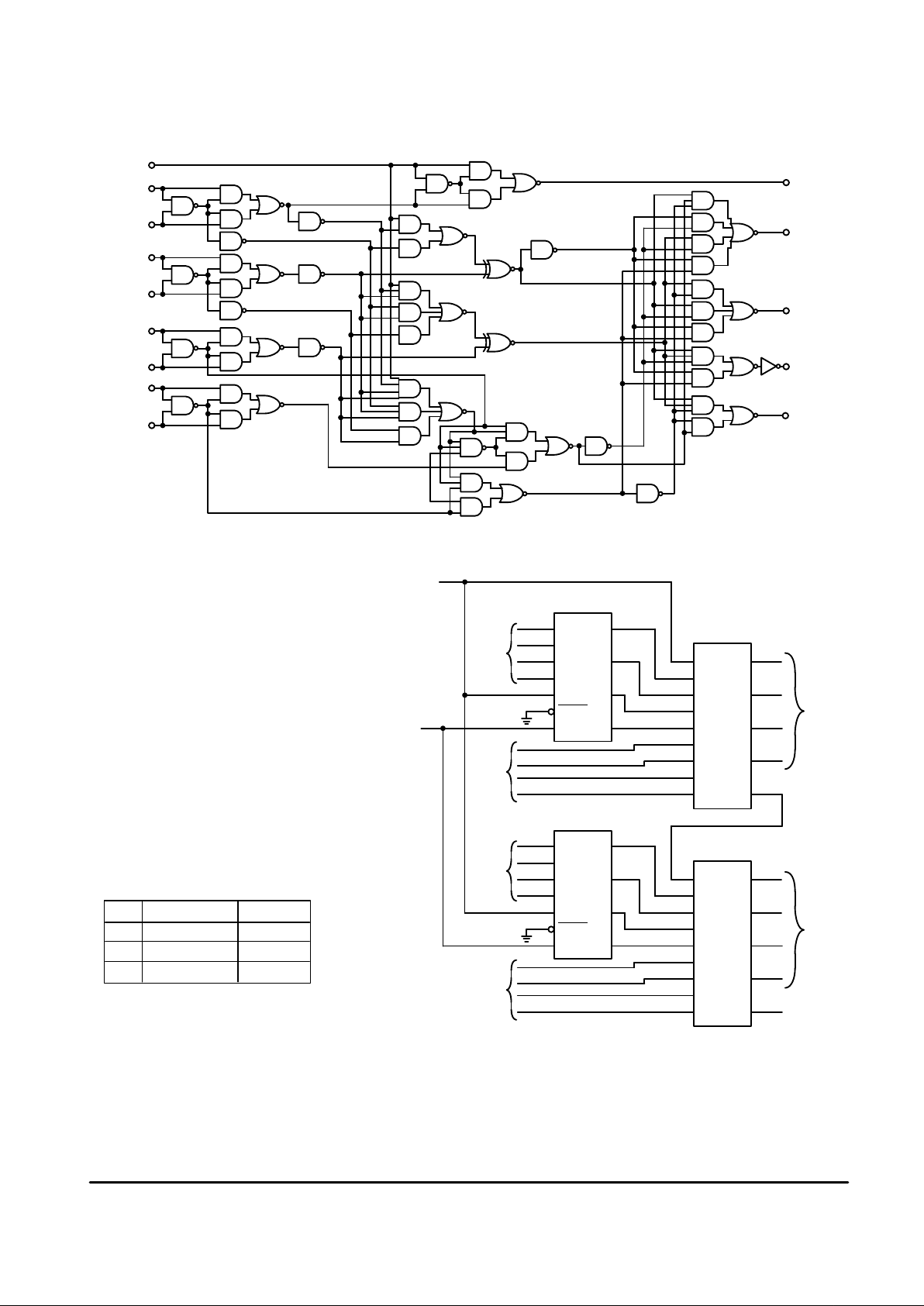
FUNCTIONAL EQUIVALENT LOGIC DIAGRAM
C
in
A1
B1
A2
B2
A3
B3
A4
B4
7
15
14
1
2
3
4
5
6
VDD = PIN 16
VSS = PIN 8
13
C
out
12
11
10
9
S4
S3
S2
S1
Figure 3. Parallel Add/Subtract Circuit
One MC14560B and MC14561B permit a
BCD digit to be added to or subtracted from
a second digit, such as in this typical configuration. A second MC14561B permits either
digit to be added to or subtracted from the
other, or either word to appear unmodified at
the output.
X = Don’t Care
Zero Add/Subtract Result
0 0 B plus A
0 1 B minus A
1 X B
TRUTH TABLE
ADD/SUBTRACT
ZERO
B10
A10
B1
A1
MC14561B
MC14561B
MC14560B
MC14560B
F1
F2
F3
F4
A1
A3
A1A4
COMP
COMP
Z
F1
F2
F3
F4
A2
A3
A4
COMP
COMP
Z
A1
C
in
A2
A2
A3
A4
B1
B2
B3
B4
S3
S2
S1
S4
C
out
UNITS
A1
C
in
A2
A3
A4
B1
B2
B3
B4
S3
S2
S1
S4
C
out
TENS
 Loading...