


Motorola MC14559BCL, MC14559BCP, MC14559BDW, MC14549BCL, MC14549BDW Datasheet
MOTOROLA CMOS LOGIC DATA
1
MC14549B MC14559B
The MC14549B and MC14559B successive approximation registers are
8–bit registers providing all the digital control and storage necessary for
successive approximation analog–to–digital conversion systems. These
parts d iffer in only one control i nput. T he Master Reset ( MR) on the
MC14549B is required in the cascaded mode when more than 8 bits are
desired. The Feed Forward (FF) of the MC14559B is used for register
shortening where End–of–Conversion (EOC) is required after less than eight
cycles.
Applications for the MC14549B and MC14559B include analog–to–digital
conversion, with serial and parallel outputs.
• Totally Synchronous Operation
• All Outputs Buffered
• Single Supply Operation
• Serial Output
• Retriggerable
• Compatible with a Variety of Digital and Analog Systems such as the
MC1408 8–Bit D/A Converter
• All Control Inputs Positive–Edge Triggered
• Supply Voltage Range = 3.0 Vdc to 18 Vdc
• Capable of Driving Two Low–Power TTL Loads, One Low–Power
Schottky TTL Load or Two HTL Loads Over the Rated Temperature
Range
• Chip Complexity: 488 FETs or 122 Equivalent Gates
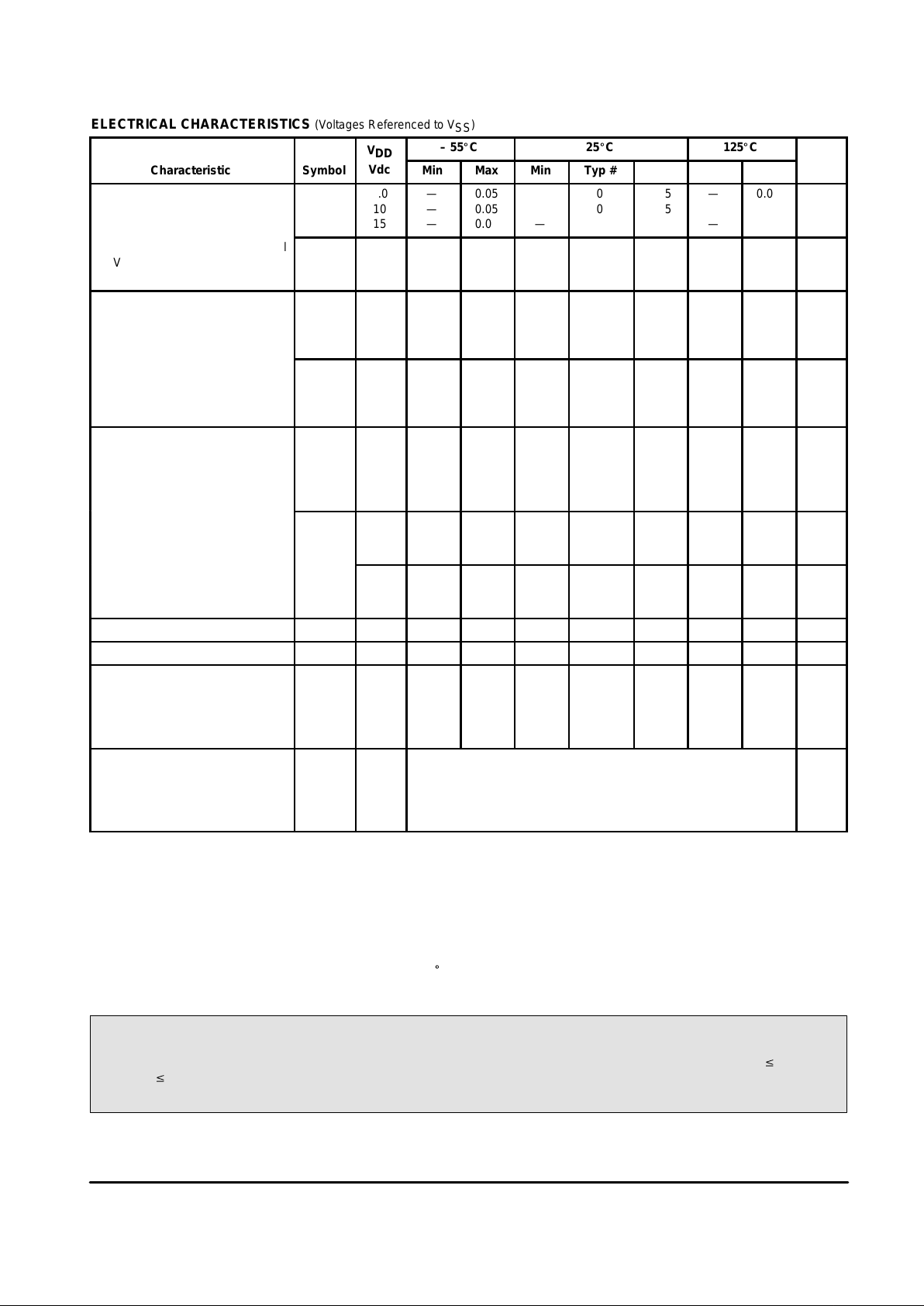
MAXIMUM RATINGS* (Voltages referenced to V
SS
)
Rating
Symbol Value Unit
DC Supply Voltage V
DD
– 0.5 to + 18 Vdc
Input Voltage, All Inputs V
in
– 0.5 to VDD + 0.5 Vdc
DC Input Current, per Pin I
in
± 10 mAdc
Power Dissipation, per Package† P
D
500 mW
Operating Temperature Range T
A
– 55 to + 125
_
C
Storage Temperature Range T
stg
– 65 to + 150
_
C
*Maximum Ratings are those values beyond which damage to the device may occur.
†Temperature Derating:
“P and D/DW” Packages: – 7.0 mW/C From 65_C To 125_C Ceramic
“L” Packages: – 12 mW/_C From 100_C To 125_C
SC SC(
t–1
) MR MR(
t–1
) Clock Action
X X X X None
X X 1 X Reset
1 0 0 0 Start
Conversion
1 X 0 1 Start
Conversion
1 1 0 0 Continue
Conversion
0 X 0 X Continue
Previous
Operation
TRUTH TABLES
MC14549B
X = Don’t Care t–1 = State at Previous Clock
SC SC(
t–1
) EOC Clock Action
X X X None
1 0 0 Start
Conversion
X 1 0 Continue
Conversion
0 0 0 Continue
Conversion
0 X 1 Retain
Conversion
Result
1 X 1 Start
Conversion
MC14559B
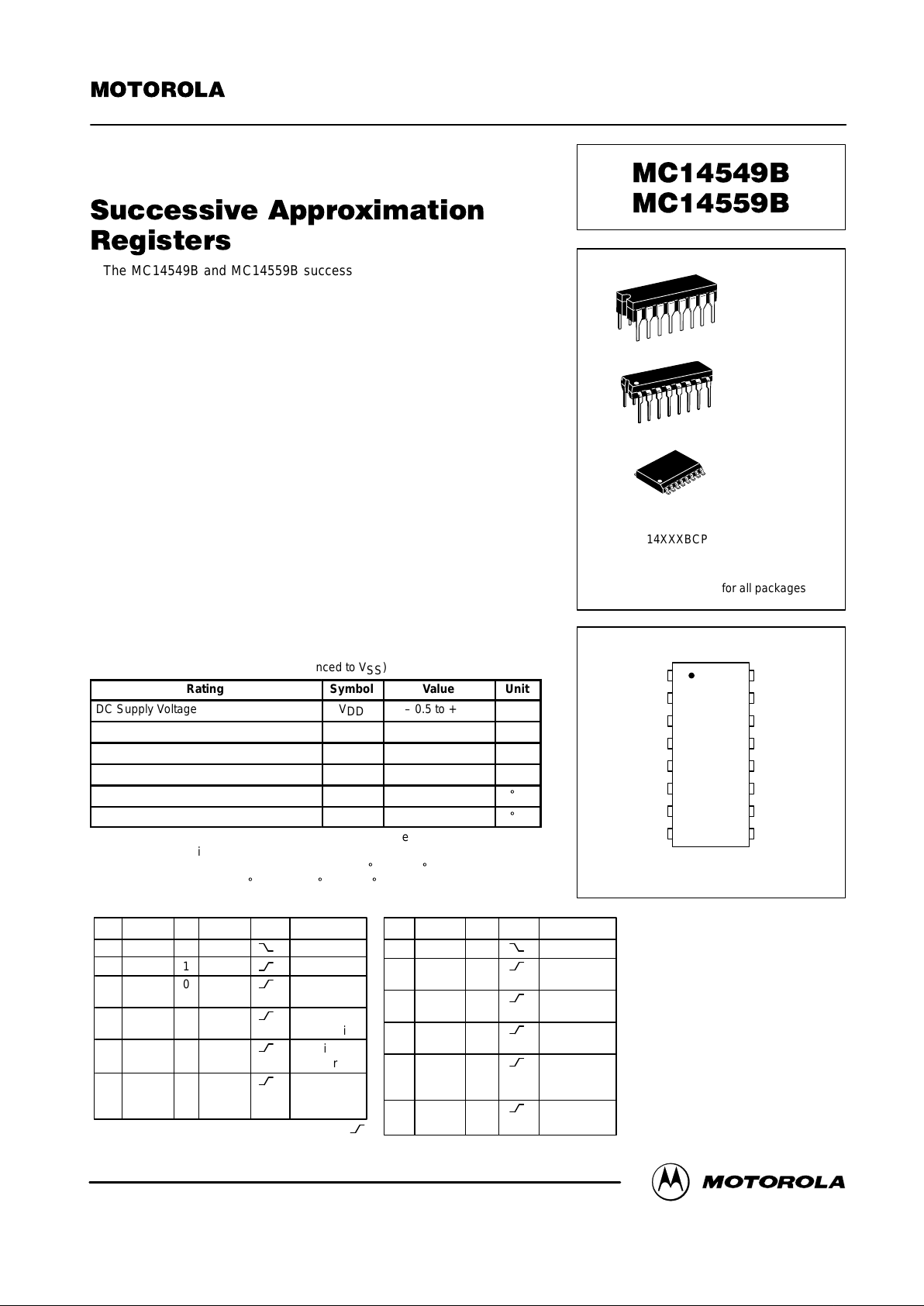
SEMICONDUCTOR TECHNICAL DATA
Motorola, Inc. 1995
REV 3
1/94
L SUFFIX
CERAMIC
CASE 620
ORDERING INFORMATION
MC14XXXBCP Plastic
MC14XXXBCL Ceramic
MC14XXXBDW SOIC
TA = – 55° to 125°C for all packages.
P SUFFIX
PLASTIC
CASE 648
DW SUFFIX
SOIC
CASE 751G
PIN ASSIGNMENT
13
14
15
16
9
10
11
125
4
3
2
1
8
7
6
Q0
Q1
Q2
Q3
V
DD
SC
*
EOC
Q7
Q6
Q5
Q4
V
SS
C
D
S
out
*For MC14549B Pin 10 is MR input.
For MC14559B Pin 10 is FF input.
MOTOROLA CMOS LOGIC DATAMC14549B MC14559B
2
ELECTRICAL CHARACTERISTICS (Voltages Referenced to V
SS
)
V
DD
– 55_C 25_C 125_C
Characteristic
Symbol
DD
Vdc
Min Max Min Typ # Max Min Max
Unit
Output Voltage “0” Level
Vin = VDD or 0
V
OL
5.0
10
15
—
—
—
0.05
0.05
0.05
—
—
—
0
0
0
0.05
0.05
0.05
—
—
—
0.05
0.05
0.05
Vdc
“1” Level
Vin = 0 or V
DD
V
OH
5.0
10
15
4.95
9.95
14.95
—
—
—
4.95
9.95
14.95
5.0
10
15
—
—
—
4.95
9.95
14.95
—
—
—
Vdc
Input Voltage # “0” Level
(VO = 4.5 or 0.5 Vdc)
(VO = 9.0 or 1.0 Vdc)
(VO = 13.5 or 1.5 Vdc)
V
IL
5.0
10
15
—
—
—
1.5
3.0
4.0
—
—
—
2.25
4.50
6.75
1.5
3.0
4.0
—
—
—
1.5
3.0
4.0
Vdc
“1” Level
(VO = 0.5 or 4.5 Vdc)
(VO = 1.0 or 9.0 Vdc)
(VO = 1.5 or 13.5 Vdc)
V
IH
5.0
10
15
3.5
7.0
11
—
—
—
3.5
7.0
11
2.75
5.50
8.25
—
—
—
3.5
7.0
11
—
—
—
Vdc
Output Drive Current
(VOH = 2.5 Vdc) Source
(VOH = 4.6 Vdc)
(VOH = 9.5 Vdc)
(VOH = 13.5 Vdc)
I
OH
5.0
5.0
10
15
– 1.2
– 0.25
– 0.62
– 1.8
—
—
—
—
– 1.0
– 0.2
– 0.5
– 1.5
– 1.7
– 0.36
– 0.9
– 3.5
—
—
—
—
– 0.7
– 0.14
– 0.35
– 1.1
—
—
—
—
mAdc
(VOL = 0.4 Vdc) Sink
(VOL = 0.5 Vdc) Q Outputs
(VOL = 1.5 Vdc)
I
OL
5.0
10
15
1.28
3.2
8.4
—
—
—
1.02
2.6
6.8
1.76
4.5
17.6
—
—
—
0.72
1.8
4.8
—
—
—
mAdc
(VOL = 0.4 Vdc) Sink
(VOL = 0.5 Vdc) Pin 5, 11 only
(VOL = 1.5 Vdc)
5.0
10
15
0.64
1.6
4.2
—
—
—
0.51
1.3
3.4
0.88
2.25
8.8
—
—
—
0.36
0.9
2.4
—
—
—
mAdc
Input Current I
in
15 — ±0.1 — ±0.00001 ±0.1 — ±1.0 µAdc
Input Capacitance C
in
— — — — 5.0 7.5 — — pF
Quiescent Current
(Per Package)
(Clock = 0 V,
Other Inputs = V
DD
or 0 V, I
out
= 0 µA)
I
DD
5.0
10
15
—
—
—
5.0
10
20
—
—
—
0.005
0.010
0.015
5.0
10
20
—
—
—
150
300
600
µAdc
Total Supply Current**†
(Dynamic plus Quiescent,
Per Package)
(CL = 50 pF on all outputs, all
buffers switching)
I
T
5.0
10
15
IT = (0.8 µA/kHz) f + I
DD
IT = (1.6 µA/kHz) f + I
DD
IT = (2.4 µA/kHz) f + I
DD
µAdc
#Noise immunity specified for worst–case input combination.
Noise Margin for both “1” and “0” level = 1.0 V min @ VDD = 5.0 V
= 2.0 V min @ VDD = 10 V
= 2.5 V min @ VDD = 15 V
†To calculate total supply current at loads other than 50 pF:
IT(CL) = IT(50 pF) + 3.5 x 10⁻³ (CL = 50) VDDf
where: IT is in µA (per package), CL in pF, VDD in V, and f in kHz is input frequency.
**The formulas given are for the typical characteristics only at 25_C.
This device contains circuitry to protect the inputs against damage due to high static voltages or electric fields; however, it
is advised that normal precautions be taken to avoid application of any voltage higher than maximum rated voltages to this
high impedance circuit. For proper operation it is recommended that Vin and V
out
be constrained to the range VSS v (Vin or
V
out
) v VDD.
Unused inputs must always be tied to an appropriate logic voltage level (e.g., either VSS or VDD).
MOTOROLA CMOS LOGIC DATA
3
MC14549B MC14559B
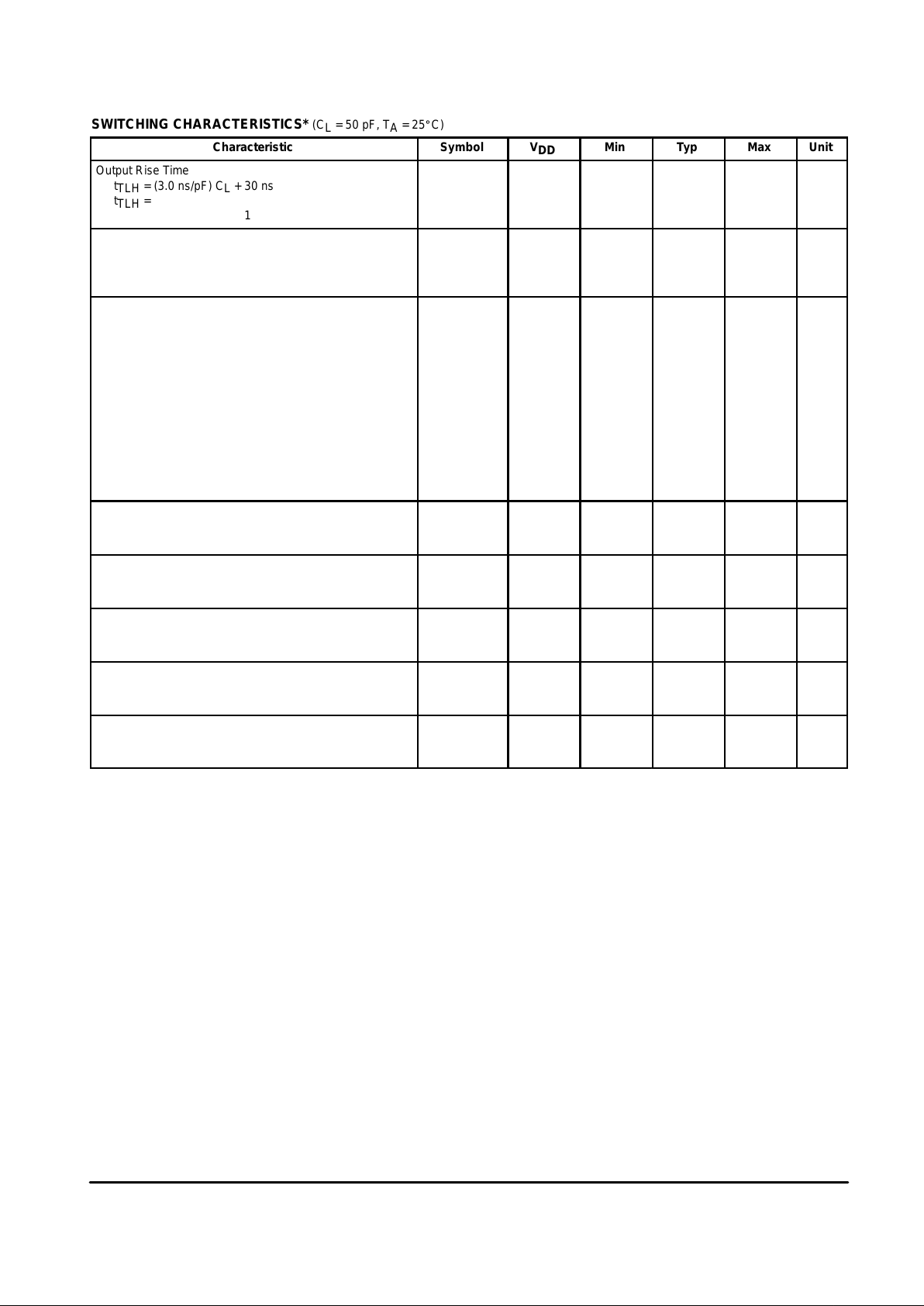
SWITCHING CHARACTERISTICS* (C
L
= 50 pF, TA = 25_C)
Characteristic
Symbol V
DD
Min Typ Max Unit
Output Rise Time
t
TLH
= (3.0 ns/pF) CL + 30 ns
t
TLH
= (1.5 ns/pF) CL + 15 ns
t
TLH
= (1.1 ns/pF) CL + 10 ns
t
TLH
5.0
10
15
—
—
—
180
90
65
360
180
130
ns
Output Fall Time
t
THL
= (1.5 ns/pF) CL + 25 ns
t
THL
= (0.75 ns/pF) CL + 12.5 ns
t
THL
= (0.55 ns/pF) CL + 9.5 ns
t
THL
5.0
10
15
—
—
—
100
50
40
200
100
80
ns
Propagation Delay Time
Clock to Q
t
PLH
, t
PHL
= (1.7 ns/pF) CL + 415 ns
t
PLH
, t
PHL
= (0.66 ns/pF) CL + 177 ns
t
PLH
, t
PHL
= (0.5 ns/pF) CL + 130 ns
Clock to S
out
t
PLH
, t
PHL
= (1.7 ns/pF) CL + 665 ns
t
PLH
, t
PHL
= (0.66 ns/pF) CL + 277 ns
t
PLH
, t
PHL
= (0.5 ns/pF) CL + 195 ns
Clock to EOC
t
PLH
, t
PHL
= (1.7 ns/pF) CL + 215 ns
t
PLH
, t
PHL
= (0.66 ns/pF) CL + 97 ns
t
PLH
, t
PHL
= (0.5 ns/pF) CL + 75 ns
t
PLH
,
t
PHL
5.0
10
15
5.0
10
15
5.0
10
15
—
—
—
—
—
—
—
—
500
210
155
750
310
220
300
130
100
1000
420
310
1500
620
440
600
260
200
ns
SC, D, FF or MR Setup Time t
su
5.0
10
15
250
100
80
125
50
40
—
—
—
ns
Clock Pulse Width t
WH(cl)
5.0
10
15
700
270
200
350
135
100
—
—
—
ns
Pulse Width — D, SC, FF or MR t
WH
5.0
10
15
500
200
160
250
100
80
—
—
—
ns
Clock Rise and Fall Time t
TLH
,
t
THL
5.0
10
15
—
—
— —
15
1.0
0.5
µs
Clock Pulse Frequency f
cl
5.0
10
15
—
—
—
1.5
3.0
4.0
0.8
1.5
2.0
MHz
*The formulas given are for the typical characteristics only.