

Motorola MC14558BCP, MC14558BD, MC14558BCL Datasheet
MOTOROLA CMOS LOGIC DATA
1
MC14558B
The MC14558B decodes 4–bit binary coded decimal data dependent on
the state of auxiliary inputs, Enable and RBI
, and provides an active–high
seven–segment output for a display driver.
An a uxiliary input truth table is shown, i n addition to t he BCD to
seven–segment truth table, to indicate the functions available with the two
auxiliary inputs.
Leading Zero blanking is easily obtained with an external flip–flop in time
division multiplexed systems displaying most significant decade first.
• Supply Voltage Range = 3.0 Vdc to 18 Vdc
• Segment Blanking for All Illegal Input Combinations
• Lamp Test Function
• Capability for Suppression of Non–Significant Zeros
• Lamp Intensity Function
• Capable of Driving Two Low–power TTL Loads. One Low–power
Schottky TTL Load or Two HTL Loads Over the Rated Temperature
Range
MAXIMUM RATINGS* (Voltages referenced to V
SS
)
Rating
Symbol Value Unit
DC Supply Voltage V
DD
– 0.5 to + 18 V
Input Voltage, All Inputs V
in
– 0.5 to VDD + 0.5 V
DC Input Voltage, per Pin I
in
± 10 mAdc
Operating Temperature Range T
A
– 55 to + 125
_
C
Power Dissipation, per Package† P
D
500 mW
Storage Temperature Range T
stg
– 65 to + 150
_
C
*Maximum Ratings are those values beyond which damage to the device may occur.
†Temperature Derating:
Plastic “P and D/DW” Packages: – 7.0 mW/_C From 65_C To 125_C
Ceramic “L” Packages: – 12 mW/_C From 100_C To 125_C
AUXILIARY INPUT TRUTH TABLE
Enable
Pin 3
RBI
Pin 5
BCD
Input
Code
RBO
Pin 4
Function Performed
0 0 X 0 Lamp Test
0 1 X 1 Blank Segments
1 1 0 1 Display Zero
1 0 0 0 Blank Segments
1 X 1 – 9 1 1–9 Displayed
X = Don’t Care
RBI
= Ripple Blanking Input
RBO
= Ripple Blanking Output
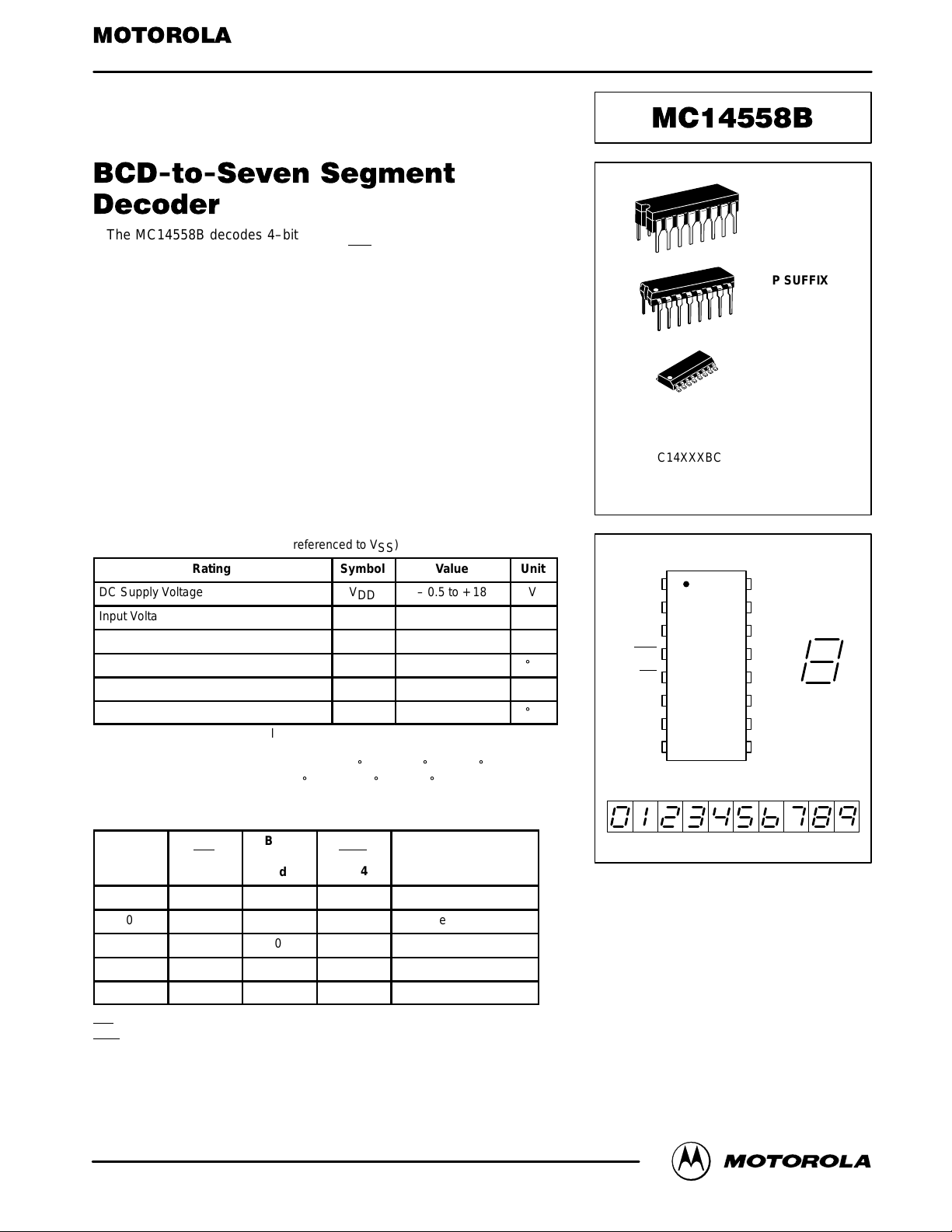
SEMICONDUCTOR TECHNICAL DATA
Motorola, Inc. 1995
REV 3
1/94
L SUFFIX
CERAMIC
CASE 620
ORDERING INFORMATION
MC14XXXBCP Plastic
MC14XXXBCL Ceramic
MC14XXXBD SOIC
TA = – 55° to 125°C for all packages.
P SUFFIX
PLASTIC
CASE 648
D SUFFIX
SOIC
CASE 751B
PIN ASSIGNMENT
13
14
15
16
9
10
11
125
4
3
2
1
8
7
6
b
a
g
f
V
DD
e
d
c
RBO
ENABLE
C
B
V
SS
A
D
RBI
a
b
c
d
e
f
g
0 1 2 3 4 5 6 7 8 9
DISPLAY
MOTOROLA CMOS LOGIC DATAMC14558B
2
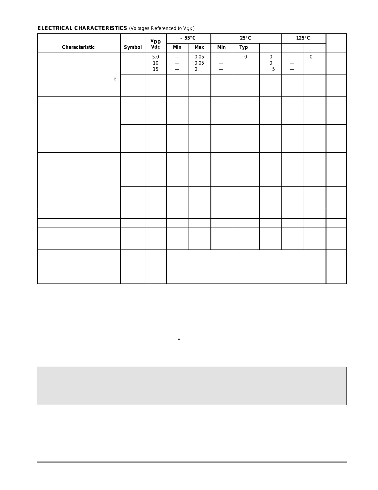
ELECTRICAL CHARACTERISTICS (Voltages Referenced to V
SS
)
V
– 55_C 25_C 125_C
Characteristic
Symbol
V
DD
Vdc
Min Max Min Typ # Max Min Max
Unit
Output Voltage “0” Level
Vin = VDD or 0
V
OL
5.0
10
15
—
—
—
0.05
0.05
0.05
—
—
—
0
0
0
0.05
0.05
0.05
—
—
—
0.05
0.05
0.05
Vdc
“1” Level
Vin = 0 or V
DD
V
OH
5.0
10
15
4.95
9.95
14.95
—
—
—
4.95
9.95
14.95
5.0
10
15
—
—
—
4.95
9.95
14.95
—
—
—
Vdc
Input Voltage “0” Level
(VO = 4.5 or 0.5 Vdc)
(VO = 9.0 or 1.0 Vdc)
(VO = 13.5 or 1.5 Vdc)
V
IL
5.0
10
15
—
—
—
1.5
3.0
4.0
—
—
—
2.25
4.50
6.75
1.5
3.0
4.0
—
—
—
1.5
3.0
4.0
Vdc
“1” Level
(VO = 0.5 or 4.5 Vdc)
(VO = 1.0 or 9.0 Vdc)
(VO = 1.5 or 13.5 Vdc)
V
IH
5.0
10
15
3.5
7.0
11
—
—
—
3.5
7.0
11
2.75
5.50
8.25
—
—
—
3.5
7.0
11
—
—
—
Vdc
Output Drive Current
(VOH = 2.5 Vdc) Source
(VOH = 4.6 Vdc)
(VOH = 9.5 Vdc)
(VOH = 13.5 Vdc)
I
OH
5.0
5.0
10
15
– 3.0
– 0.64
– 1.6
– 4.2
—
—
—
—
– 2.4
– 0.51
– 1.3
– 3.4
– 4.2
– 0.88
– 2.25
– 8.8
—
—
—
—
– 1.7
– 0.36
– 0.9
– 2.4
—
—
—
—
mAdc
(VOL = 0.4 Vdc) Sink
(VOL = 0.5 Vdc)
(VOL = 1.5 Vdc)
I
OL
5.0
10
15
0.64
1.6
4.2
—
—
—
0.51
1.3
3.4
0.88
2.25
8.8
—
—
—
0.36
0.9
2.4
—
—
—
mAdc
Input Current I
in
15 — ±0.1 — ±0.00001 ±0.1 — ±1.0 µAdc
Input Capacitance C
in
— — — — 5.0 7.5 — — pF
Quiescent Current
(Per Package) Vin = 0 or V
DD
I
out
= 0 µA
I
DD
5.0
10
15
—
—
—
5.0
10
20
—
—
—
0.005
0.010
0.015
5.0
10
20
—
—
—
150
300
600
µAdc
Total Supply Current**†
(Dynamic plus Quiescent,
Per Package)
(CL = 50 pF on all outputs, all
buffers switching)
I
T
5.0
10
15
IT = (1.2 µA/kHz) f + I
DD
IT = (2.4 µA/kHz) f + I
DD
IT = (3.6 µA/kHz) f + I
DD
µAdc
#Noise immunity specified for worst–case input combination.
Noise Margin for both “1” and “0” level = 1.0 V min @ VDD = 5.0 V
= 2.0 V min @ VDD = 10 V
= 2.5 V min @ VDD = 15 V
†To calculate total supply current at loads other than 50 pF:
IT(CL) = IT(50 pF) + 3.5 x 10⁻³ (CL – 50) VDDf
where: IT is in µA (per package), CL in pF, VDD in V, and f in kHz is input frequency.
**The formulas given are for the typical characteristics only at 25_C.
This device contains circuitry to protect the inputs against damage due to high static voltages or electric fields; however,
it is advised that normal precautions be taken to avoid applications of any voltage higher than maximum rated voltages to this
high-impedance circuit. For proper operation it is recommended that Vin and V
out
be constrained to the range VSS ≤ (Vin or
V
out
) ≤ VDD.
Unused inputs must always be tied to an appropriate logic voltage level (e.g., either VSS or VDD).
MOTOROLA CMOS LOGIC DATA
3
MC14558B
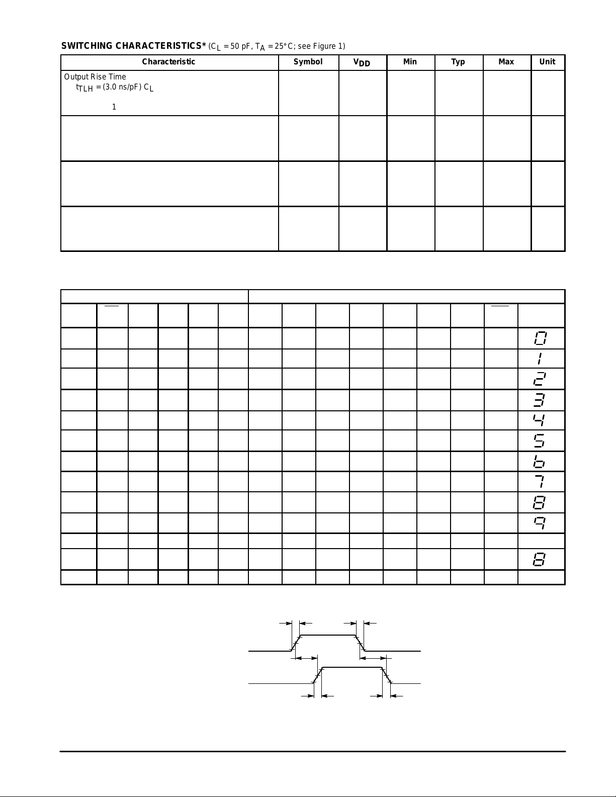
SWITCHING CHARACTERISTICS* (C
L
= 50 pF, TA = 25_C; see Figure 1)
Characteristic
Symbol V
DD
Min Typ Max Unit
Output Rise Time
t
TLH
= (3.0 ns/pF) CL + 30 ns
t
TLH
= (1.5 ns/pF) CL + 15 ns
t
TLH
= (1.1 ns/pF) CL + 10 ns
t
TLH
5.0
10
15
—
—
—
100
50
40
200
100
80
ns
Output Fall Time
t
THL
= (1.5 ns/pF) CL + 25 ns
t
THL
= (0.75 ns/pF) CL + 12.5 ns
t
THL
= (0.55 ns/pF) CL + 9.5 ns
t
THL
5.0
10
15
—
—
—
100
50
40
200
100
80
ns
Propagation Delay Time
t
PLH
= (1.7 ns/pF) CL + 495 ns
t
PLH
= (0.66 ns/pF) CL + 187 ns
t
PLH
= (0.5 ns/pF) CL + 120 ns
t
PLH
5.0
10
15
—
—
—
580
220
145
1160
440
230
ns
Propagation Delay Time
t
PHL
= (1.7 ns/pF) CL + 695 ns
t
PHL
= (0.66 ns/pF) CL + 242 ns
t
PHL
= (0.5 ns/pF) CL + 160 ns
t
PHL
5.0
10
15
—
—
780
275
185
1560
550
370
ns
*The formulae given are for the typical characteristics only.
TRUTH TABLE
Inputs Outputs*
Enable
Pin 3
RBI
Pin 5
D
Pin 6CPin 2BPin 1APin 7aPin 13bPin 12cPin 11dPin 10ePin 9fPin 15gPin 14
RBO
Pin 4
Display
1 1 0 0 0 0 1 1 1 1 1 1 0 1
1 X 0 0 0 1 0 0 0 0 1 1 0 1
1 X 0 0 1 0 1 1 0 1 1 0 1 1
1 X 0 0 1 1 1 1 1 1 0 0 1 1
1 X 0 1 0 0 0 1 1 0 0 1 1 1
1 X 0 1 0 1 1 0 1 1 0 1 1 1
1 X 0 1 1 0 0 0 1 1 1 1 1 1
1 X 0 1 1 1 1 1 1 0 0 0 0 1
1 X 1 0 0 0 1 1 1 1 1 1 1 1
1 X 1 0 0 1 1 1 1 0 0 1 1 1
1 0 0 0 0 0 0 0 0 0 0 0 0 0 Blank
0 0 X X X X 1 1 1 1 1 1 1 0
0 1 X X X X 0 0 0 0 0 0 0 1 Blank
*All non–valid BCD input codes produce a blank display.
X = Don’t Care
Figure 1. Signal Waveforms
20 ns 20 ns
10%
90%
50%
t
PLH
t
PHL
50%
10%
90%
t
TLH
t
THL
ANY OUTPUT
ANY INPUT
 Loading...