

MOTOROLA MC14557BCP, MC14557BDW, MC14557BDWR2, MC14557BF, MC14557BFEL Datasheet
...
Semiconductor Components Industries, LLC, 2000
March, 2000 – Rev. 3
1 Publication Order Number:
MC14557B/D
MC14557B
1-to-64 Bit V ariable Length
Shift Register
The MC14557B is a static clocked serial shift register whose length
may be programmed to be any number of bits between 1 and 64. The
number of bits selected is equal to the sum of the subscripts of the
enabled Length Control inputs (L1, L2, L4, L8, L16, and L32) plus
one. Serial data may be selected from the A or B data inputs with the
A/B select input. This feature is useful for recirculation purposes. A
Clock Enable (CE) input is provided to allow gating of the clock or
negative edge clocking capability .
The device can be effectively used for variable digital delay lines or
simply to implement odd length shift registers.
• 1–64 Bit Programmable Length
• Q and Q Serial Buffered Outputs
• Asynchronous Master Reset
• All Inputs Buffered
• No Limit On Clock Rise and Fall T imes
• Supply Voltage Range = 3.0 Vdc to 18 Vdc
• Capable of Driving Two Low–power TTL Loads or one Low–power
Schottky TTL Load Over the Rated Temperature Range
MAXIMUM RATINGS (Voltages Referenced to V
SS
) (Note 2.)
Symbol
Parameter Value Unit
V
DD
DC Supply Voltage Range –0.5 to +18.0 V
Vin, V
out
Input or Output Voltage Range
(DC or Transient)
–0.5 to VDD + 0.5 V
Iin, I
out
Input or Output Current
(DC or Transient) per Pin
±10 mA
P
D
Power Dissipation,
per Package (Note 3.)
500 mW
T
A
Ambient Temperature Range –55 to +125 °C
T
stg
Storage Temperature Range –65 to +150 °C
T
L
Lead Temperature
(8–Second Soldering)
260 °C
2. Maximum Ratings are those values beyond which damage to the device
may occur.
3. T emperature Derating:
Plastic “P and D/DW” Packages: – 7.0 mW/_C From 65_C T o 125_C
This device contains protection circuitry to guard against damage due to high
static voltages or electric fields. However, precautions must be taken to avoid
applications of any voltage higher than maximum rated voltages to this
high–impedance circuit. For proper operation, V
in
and V
out
should be constrained
to the range V
SS
v (Vin or V
out
) v VDD.
Unused inputs must always be tied to an appropriate logic voltage level (e.g.,
either V
SS
or VDD). Unused outputs must be left open.
http://onsemi.com
A = Assembly Location
WL or L = Wafer Lot
YY or Y = Year
WW or W = Work Week
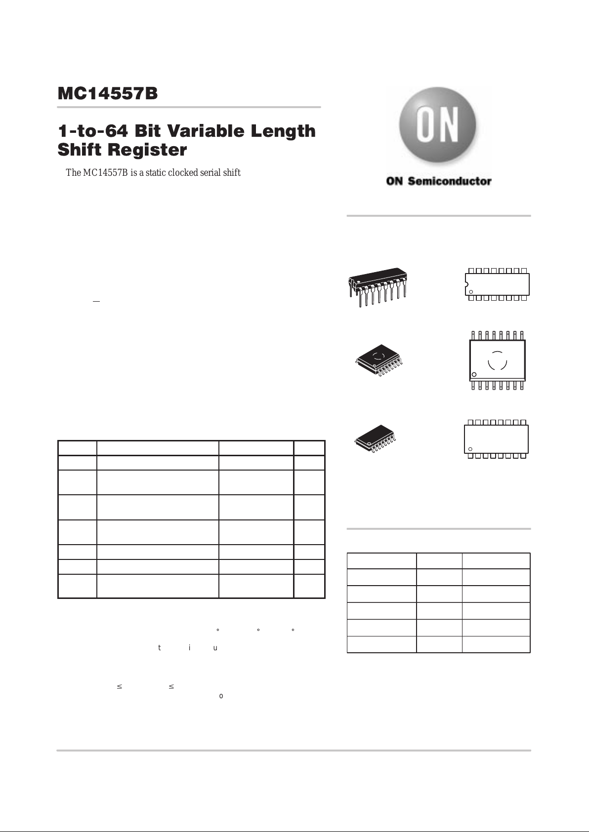
Device Package Shipping
ORDERING INFORMATION
MC14557BCP PDIP–16 2000/Box
MC14557BDW SOIC–16 47/Rail
MARKING
DIAGRAMS
1
16
PDIP–16
P SUFFIX
CASE 648
MC14557BCP
AWLYYWW
SOIC–16
DW SUFFIX
CASE 751G
1
16
14557B
AWLYYWW
MC14557BDWR2 SOIC–16 1000/Tape & Reel
MC14557BF SOEIAJ–16 See Note 1.
MC14557BFEL SOEIAJ–16 See Note 1.
1. For ordering information on the EIAJ version of
the SOIC packages, please contact your local
ON Semiconductor representative.
SOEIAJ–16
F SUFFIX
CASE 966
1
16
MC14557B
AWLYWW
MC14557B
http://onsemi.com
2
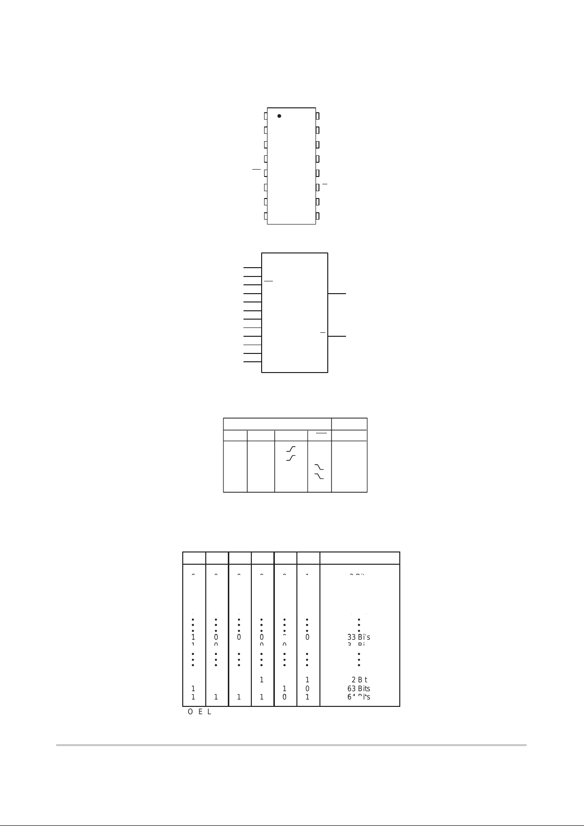
PIN ASSIGNMENT
13
14
15
16
9
10
11
125
4
3
2
1
8
7
6
L32
L16
L8
L4
V
DD
A/B SEL
Q
Q
CLOCK
RESET
L1
L2
V
SS
A
B
CE
BLOCK DIAGRAM
TRUTH TABLE
Inputs Output
Rst A/B Clock CE
Q
00 0 B
01 0 A
00 1 B
01 1 A
1X X X 0
Q is the output of the first selected shift
register stage.
X = Don’t Care
12
13
14
1
15
2
9
7
6
5
4
3
11
10
RESET
CLOCK
CE
B
A
A/B SELECT
L1
L2
L4
L8
L16
L32
Q
Q
VDD = PIN 16
V
SS
= PIN 8
LENGTH SELECT TRUTH TABLE
L32 L16 L8 L4 L2 L1 Register Length
0
0
0
0
0
0
1 Bit
0
0
0
0
0
1
2 Bits
0000103 Bit
s
0000114 Bits
0000001100015 Bits
6 Bits
0001016 Bits
1
0
0
0
0
0
33 Bits
10000134 Bit
s
111100
61 Bits
1 1 1 1 1 1 62 Bits
1
1
1
1
1
0
63 Bits
11110164 Bi
ts
NOTE: Length equals the sum of the binary length control
subscripts plus one.
MC14557B
http://onsemi.com
3
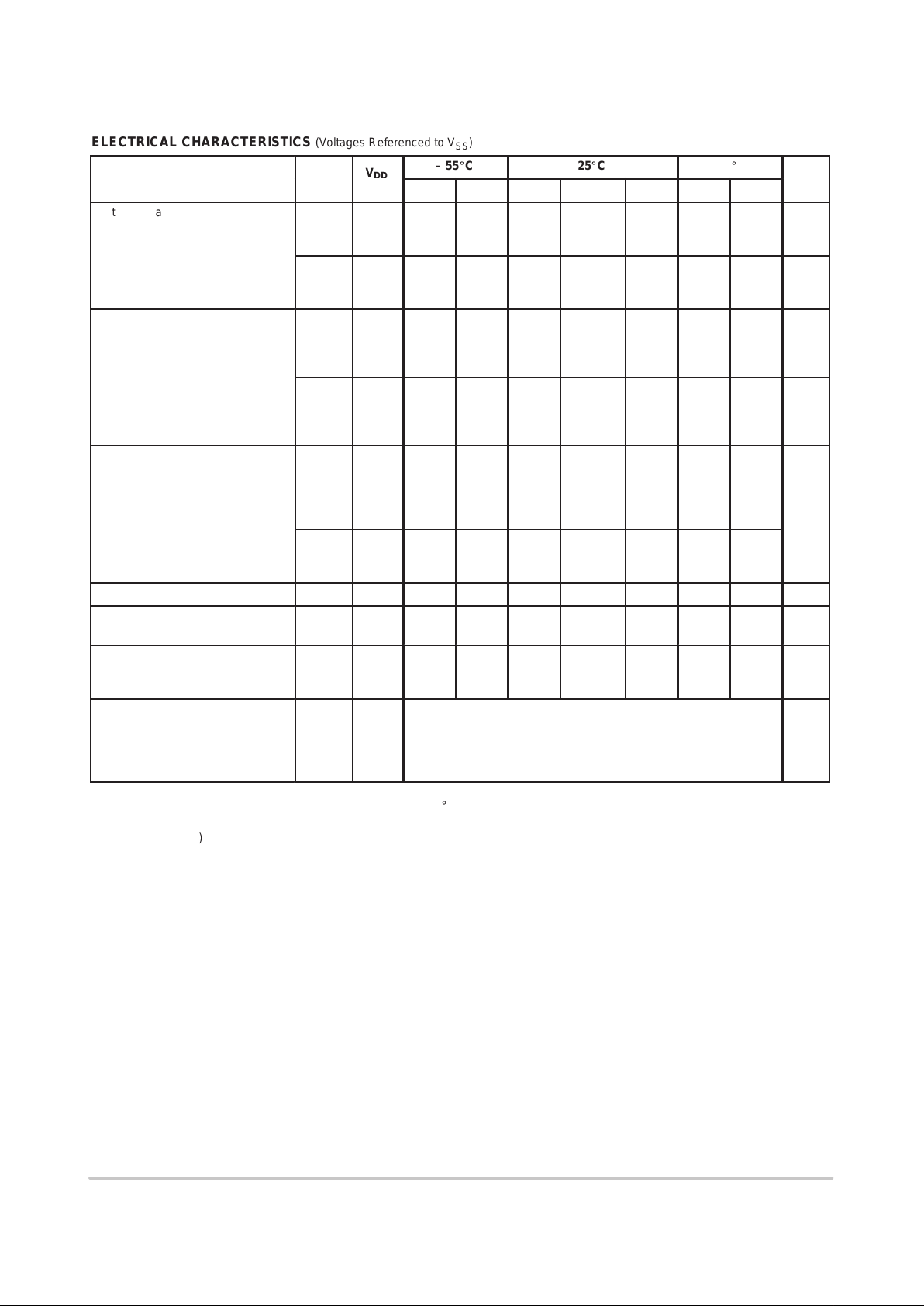
ELECTRICAL CHARACTERISTICS (Voltages Referenced to V
SS
)
V
– 55_C 25_C 125_C
Characteristic Symbol
V
DD
Vdc
Min Max Min Typ
(4.)
Max Min Max
Unit
Output Voltage “0” Level
V
in
= VDD or 0
V
OL
5.0
10
15
—
—
—
0.05
0.05
0.05
—
—
—
0
0
0
0.05
0.05
0.05
—
—
—
0.05
0.05
0.05
Vdc
“1” Level
V
in
= 0 or V
DD
V
OH
5.0
10
15
4.95
9.95
14.95
—
—
—
4.95
9.95
14.95
5.0
10
15
—
—
—
4.95
9.95
14.95
—
—
—
Vdc
Input Voltage “0” Level
(V
O
= 4.5 or 0.5 Vdc)
(V
O
= 9.0 or 1.0 Vdc)
(V
O
= 13.5 or 1.5 Vdc)
V
IL
5.0
10
15
—
—
—
1.5
3.0
4.0
—
—
—
2.25
4.50
6.75
1.5
3.0
4.0
—
—
—
1.5
3.0
4.0
Vdc
“1” Level
(V
O
= 0.5 or 4.5 Vdc)
(V
O
= 1.0 or 9.0 Vdc)
(V
O
= 1.5 or 13.5 Vdc)
V
IH
5.0
10
15
3.5
7.0
11
—
—
—
3.5
7.0
11
2.75
5.50
8.25
—
—
—
3.5
7.0
11
—
—
—
Vdc
Output Drive Current
(V
OH
= 2.5 Vdc) Source
(V
OH
= 4.6 Vdc)
(V
OH
= 9.5 Vdc)
(V
OH
= 13.5 Vdc)
I
OH
5.0
5.0
10
15
– 3.0
– 0.64
– 1.6
– 4.2
—
—
—
—
– 2.4
– 0.51
– 1.3
– 3.4
– 4.2
– 0.88
– 2.25
– 8.8
—
—
—
—
– 1.7
– 0.36
– 0.9
– 2.4
—
—
—
—
mAdc
(VOL = 0.4 Vdc) Sink
(V
OL
= 0.5 Vdc)
(V
OL
= 1.5 Vdc)
I
OL
5.0
10
15
0.64
1.6
4.2
—
—
—
0.51
1.3
3.4
0.88
2.25
8.8
—
—
—
0.36
0.9
2.4
—
—
—
Input Current I
in
15 — ±0.1 — ±0.00001 ±0.1 — ±1.0 µAdc
Input Capacitance
(V
in
= 0)
C
in
— — — — 5.0 7.5 — — pF
Quiescent Current
(Per Package)
I
DD
5.0
10
15
—
—
—
5.0
10
20
—
—
—
0.010
0.020
0.030
5.0
10
20
—
—
—
150
300
600
µAdc
Total Supply Current
(5.) (6.)
(Dynamic plus Quiescent,
Per Package)
(C
L
= 50 pF on all outputs, all
buffers switching)
I
T
5.0
10
15
IT = (1.75 µA/kHz) f + I
DD
IT = (3.50 µA/kHz) f + I
DD
IT = (5.25 µA/kHz) f + I
DD
µAdc
4. Data labelled “T yp” is not to be used for design purposes but is intended as an indication of the IC’s potential performance.
5. The formulas given are for the typical characteristics only at 25_C.
6. To calculate total supply current at loads other than 50 pF:
I
T(CL
) = IT(50 pF) + (CL – 50) Vfk
where: I
T
is in µA (per package), CL in pF, V = (VDD – VSS) in volts, f in kHz is input frequency, and k = 0.001.
 Loading...