

Motorola MC145564P, MC145567DW, MC145567L, MC145564DW, MC145564L Datasheet
...
MC145554•MC145557•MC145564•MC145567MOTOROLA
1
The MC145554, MC145557, MC145564, and MC145567 are all per channel
PCM Codec–Filters. These devices perform the voice digitization and
reconstruction as well as the band limiting and smoothing required for PCM
systems. They are designed to operate in both synchronous and asynchronous
applications and contain a n on–chip p recision v oltage reference. The
MC145554 (Mu–Law) and MC145557 (A–Law) are general purpose devices
that are offered in 16–pin packages. The MC145564 (Mu–Law) and MC145567
(A–Law), offered in 20–pin packages, add the capability of analog loopback and
push–pull power amplifiers with adjustable gain.
These devices have an input operational amplifier whose output is the input
to the encoder section. The encoder section immediately low–pass filters the
analog signal with an active R–C filter to eliminate very–high–frequency noise
from being modulated down to the pass band by the switched capacitor filter.
From the active R–C filter, the analog signal is converted to a dif ferential signal.
From this point, all analog signal processing is done differentially. This allows
processing of an analog signal that is twice t he amplitude allowed by a
single–ended design, which r educes the significance of n oise to both t he
inverted and non–inverted signal paths. Another advantage of this differential
design is that noise injected via the power supplies is a common–mode signal
that is cancelled when the inverted and non–inverted signals are recombined.
This dramatically improves the power supply rejection ratio.
After the differential converter, a differential switched capacitor filter band
passes the analog signal from 200 Hz to 3400 Hz before the signal is digitized
by the differential compressing A/D converter.
The decoder accepts PCM data and expands it using a differential D/A
converter. The output of the D/A is low–pass filtered at 3400 Hz and sinX/X
compensated by a differential switched capacitor filter . The signal is then filtered
by an active R–C filter to eliminate the out–of–band energy of the switched
capacitor filter.
These PCM Codec–Filters accept both long–frame and short–frame industry
standard clock formats. They also maintain compatibility with Motorola’s family
of TSACs and MC3419/MC34120 SLIC products.
The MC145554/57/64/67 family of PCM Codec–Filters utilizes CMOS due to
its reliable low–power performance and proven capability f or complex
analog/digital VLSI functions.
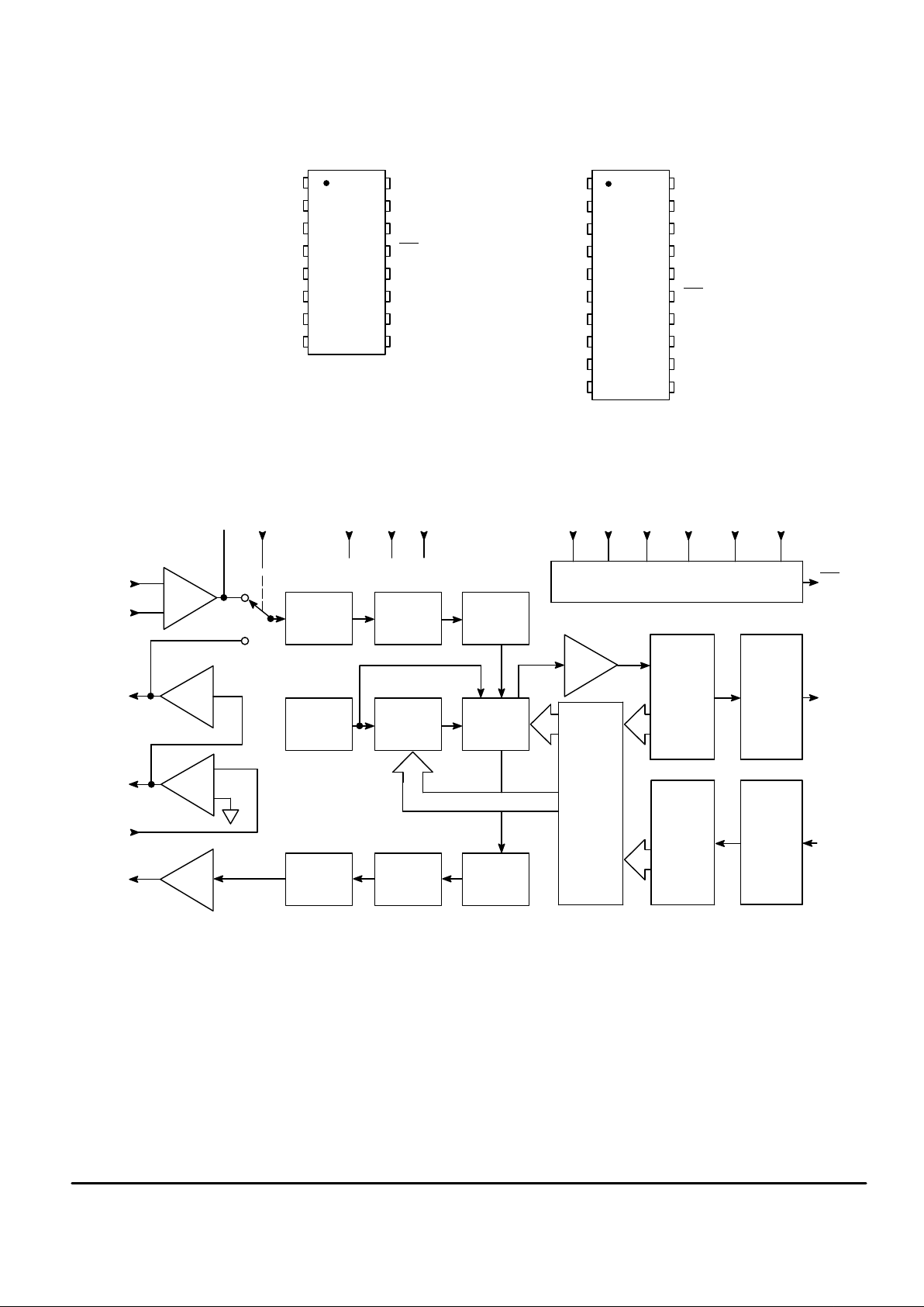
MC145554/57 (16–Pin Package)
• Fully Differential Analog Circuit Design for Lowest Noise
• Performance Specified for Extended Temperature Range of – 40 to + 85°C
• Transmit Band–Pass and Receive Low–Pass Filters On–Chip
• Active R–C Pre–Filtering and Post–Filtering
• Mu–Law Companding MC145554
• A–Law Companding MC145557
• On–Chip Precision Voltage Reference (2.5 V)
• Typical Power Dissipation of 40 mW, Power Down of 1.0 mW at ± 5 V
MC145564/67 (20–Pin Package) — All of the Features of the MC145554/57 Plus:
• Mu–Law Companding MC145564
• A–Law Companding MC145567
• Push–Pull Power Drivers with External Gain Adjust
• Analog Loopback
Order this document
by MC145554/D
SEMICONDUCTOR TECHNICAL DATA
L SUFFIX
CERAMIC PACKAGE
CASE 620
MC145554/57
P SUFFIX
PLASTIC DIP
CASE 648
MC145554/57
16
1
16
1
20
1
L SUFFIX
CERAMIC PACKAGE
CASE 732
MC145564/67
20
1
P SUFFIX
PLASTIC DIP
CASE 738
MC145564/67
DW SUFFIX
SOG PACKAGE
CASE 751G
MC145554/57
DW SUFFIX
SOG PACKAGE
CASE 751D
MC145564/67
16
1
20
1
Motorola, Inc. 1995
REV 1
9/95 (Replaces ADI1517)
MC145554•MC145557•MC145564•MC145567 MOTOROLA
2
PIN ASSIGNMENTS
MC145554, MC145557 MC145564, MC145567
13
14
15
16
9
10
11
125
4
3
2
1
8
7
6
TS
X
GS
X
VFXI–
MCLK
X
BCLK
X
D
X
V
CC
VFRO
GNDA
MCLKR/PDN
BCLKR/CLKSEL
D
R
FS
R
V
BB
VFXI+
FS
X
VPI
VPO –
GNDA
VPO+
5
4
3
2
1
10
9
8
7
6
14
15
16
17
18
19
20
11
12
13
ANLB
V
BB
TS
X
MCLK
X
BCLK
X
D
X
FS
X
GS
X
VFXI–
VFXI+
V
CC
VFRO
MCLKR/PDN
BCLKR/CLKSEL
D
R
FS
R
FUNCTIONAL BLOCK DIAGRAM
*MC145564 and MC145567 only.
GS
X
ANLB* V
CC
GNDA V
BB
FSXFSRMCLKXBCLK
X
MCLKR/
PDN
BCLKR/
CLKSEL
TS
X
D
X
D
R
RECEIVE
SHIFT
REG
RECEIVE
LATCH
MUX
S/H
5–POLE SC
LOW–PASS
FILTER
RC ACTIVE
LOW–PASS
FILTER
VFRO
VPI*
–1
VPO–
*
VPO+
*
VFXI+
VFXI–
8
4
8
SAR
REG
TRANSMIT
SHIFT
REG
4
CDACRDAC
BAND–GAP
VOLTAGE
REF
COMP
RC ACTIVE
LOW–PASS
FILTER
5–POLE SC
LOW–PASS
FILTER
3–POLE
HIGH–PASS
AND S/H
INTERNAL SEQUENCING
AND CONTROL
+
–
+
–

MC145554•MC145557•MC145564•MC145567MOTOROLA
3
DEVICE DESCRIPTION
A codec–filter is used for digitizing and reconstructing the
human voice. These devices were developed primarily for
the telephone network to facilitate voice switching and transmission. Once the voice is digitized, it may be switched by
digital switching methods or transmitted long distance (T1,
microwave, satellites, etc.) without degradation. The name
codec is an acronym from “COder” (for the A/D used to digitize voice) and “DECoder” (for the D/A used for reconstructing voice). A codec is a single device that does both the A/D
and D/A conversions.
To digitize intelligible voice requires a signal–to–distortion
ratio of about 30 dB over a dynamic range of about 40 dB.
This can be accomplished with a linear 13–bit A/D and D/A,
but will far exceed the required signal–to–distortion ratio at
amplitudes greater than 40 dB below the peak amplitude.
This excess performance is at the expense of data per sample. Methods of data reduction are implemented by compressing the 13–bit linear scheme t o companded 8–bit
schemes. T here are t wo companding schemes used:
Mu–255 Law specifically i n North America, and A–Law
specifically in E urope. These companding schemes a re
accepted world wide. These companding schemes follow a
segmented or “piecewise–linear” curve formatted as sign bit,
three chord bits, and four step bits. For a given chord, all sixteen of the steps have the same voltage weighting. As the
voltage of the analog input increases, the four step bits increment and carry to the three chord bits which increment.
When the chord bits increment, the step bits double their
voltage weighting. This results in an effective resolution of six
bits (sign + chord + four step bits) across a 42 dB dynamic
range (seven chords a bove z ero, by 6 d B per c hord).
Tables 3 and 4 show the linear quantization levels to PCM
words for the two companding schemes.
In a sampling environment, Nyquist theory says that to
properly sample a continuous signal, it must be sampled at a
frequency higher than twice the signal’s highest frequency
component. Voice contains spectral energy above 3 kHz, but
its absence is not detrimental to intelligibility. To reduce the
digital data rate, which is proportional to the sampling rate, a
sample rate of 8 kHz was adopted, consistent with a bandwidth of 3 kHz. This sampling requires a low–pass filter to
limit the high frequency energy above 3 kHz from distorting
the in–band signal. The telephone line is also subject to
50/60 Hz power line coupling, which must be attenuated from
the signal by a high–pass filter before the A/D converter.
The D/A process reconstructs a staircase version of the
desired in–band signal, which has spectral images of the in–
band signal modulated about the sample frequency and its
harmonics. These spectral images, called aliasing components, need to be attenuated to obtain the desired signal.
The low–pass filter used to attenuate these aliasing components is typically called a reconstruction or smoothing filter.
The MC145554/57/64/67 PCM Codec–Filters have the
codec, both presampling and reconstruction filters, and a
precision voltage reference on–chip, and require no external
components.
PIN DESCRIPTION
DIGITAL
FS
R
Receive Frame Sync
This is an 8 kHz enable that must be synchronous with
BCLKR. Following a rising FSR edge, a serial PCM word at
DR is clocked by BCLKR into the receive data register. FS
R
also initiates a decode on the previous PCM word. In the absence of FSX, the length of the FSR pulse is used to determine whether the I/O conforms to the Short Frame Sync or
Long Frame Sync convention.
DR
Receive Digital Data Input
BCLKR/CLKSEL
Receive Data Clock and Master Clock Frequency
Selector
If this input is a clock, it must be between 128 kHz and
4.096 MHz, and synchronous with FSR. In synchronous
applications this pin may be held at a constant level; then
BCLKX is used as the data clock for both the transmit and
receive sides, and this pin selects the assumed frequency of
the master clock (see Table 1 in Functional Description).
MCLKR/PDN
Receive Master Clock and Power–Down Control
Because of the shared DAC architecture used on these
devices, only one master clock is needed. Whenever FSX is
clocking, MCLKX is used to derive all internal clocks, and the
MCLKR/PDN pin merely serves as a power–down control. If
MCLKR/PDN pin is held low or is clocked (and at least one
of the frame syncs is present), the part is powered up. If this
pin is held high, the part is powered down. If FSX is absent
but FSR is still clocking, the device goes into receive half–
channel mode, a nd MCLKR (if c locking) generates the
internal clocks.
MCLK
X
Transmit Master Clock
This clock is used to derive the internal sequencing clocks;
it must be 1.536 MHz, 1.544 MHz, or 2.048 MHz.
BCLK
X
Transmit Data Clock
BCLKX may be any frequency between 1 28 kHz and
4.096 MHz, but it should be synchronous with MCLKX.
D
X
Transmit Digital Data Output
This output is controlled by FSX and BCLKX to output the
PCM data word; otherwise this pin is in a high–impedance
state.
FS
X
Transmit Frame Sync
This is an 8 kHz enable that must be synchronous with
BCLKX. A rising FSX edge initiates the transmission of a

MC145554•MC145557•MC145564•MC145567 MOTOROLA
4
serial PCM word, clocked by BCLKX, out of DX. If the FS
X
pulse is high for more than eight BCLKX periods, the DX and
TS
X
outputs will remain in a low–impedance state until FS
X
is brought low. The length of the FSX pulse is used to determine whether the transmit and receive digital I/O conforms to
the Short Frame Sync or to the Long Frame Sync convention.
TS
X
Transmit Time Slot Indicator
This is an open–drain output that goes low whenever the
DX output is in a low–impedance state (i.e., during the transmit time slot when the PCM word is being output) for enabling a PCM bus driver.
ANLB
Analog Loopback Control Input (MC145564/67 Only)
When held high, this pin causes the input of the transmit
RC active filter to be disconnected from GSX and connected
to VPO+ for analog loopback testing. This pin is held low in
normal operation.
ANALOG
GS
X
Gain–Setting Transmit
This output of the transmit gain–adjust operational amplifier is i nternally c onnected to t he encoder section of t he
device. It must be used in conjunction with VFXI– and VFXI+
to set the transmit gain for a maximum signal amplitude of
2.5 V peak. This output can drive a 600 Ω load to 2.5 V peak.
VFXI–
Voice–Frequency Transmit Input (Inverting)
This is the inverting input of t he transmit gain–adjust
operational amplifier.
VFXI+
Voice–Frequency Transmit Input
(Non–Inverting)
This is the non–inverting input of the transmit gain–adjust
operational amplifier.
VFRO
Voice–Frequency Receive Output
This receive analog output is capable of driving a 600 Ω
load to 2.5 V peak.
VPI
Voltage Power Input (MC145564/67 Only)
This is the inverting input to the first receive power amplifier. Both of the receive power amplifiers can be powered
down by connecting this input to VBB.
VPO–
Voltage Power Output (Inverted) (MC145564/67 Only)
This inverted output of the receive push–pull power amplifiers can drive 300 Ω to 3.3 V peak.
VPO+
Voltage Power Output (Non–Inverted)
(MC145554/67 Only)
This non–inverted output of the receive push–pull power
amplifier pair can drive 300 Ω to 3.3 V peak.
POWER SUPPLY
GNDA
Analog Ground
This terminal is the reference level for all signals, both ana-
log and digital. It is 0 V.
V
CC
Positive Power Supply
VCC is typically 5 V.
V
BB
Negative Power Supply
VBB is typically – 5 V.
FUNCTIONAL DESCRIPTION
ANALOG INTERFACE AND SIGNAL PATH
The transmit portion of these codec–filters includes a low–
noise gain setting amplifier capable of driving a 600 Ω load.
Its output is fed to a three–pole anti–aliasing pre–filter. This
pre–filter incorporates a two–pole Butterworth active low–
pass filter, and a single passive pole. This pre–filter is followed by a single e nded–to–differential converter that is
clocked at 256 kHz. All subsequent analog processing utilizes fully differential circuitry. The next section is a fully–differential, five–pole switched capacitor low–pass filter with a
3.4 kHz passband. After this filter is a 3–pole switched–capacitor high–pass filter having a cutoff frequency of about
200 Hz. This high–pass stage has a transmission zero at dc
that eliminates any dc coming from the analog input or from
accumulated operational amplifier offsets in the preceding filter stages. The last stage of the high–pass filter is an autozeroed sample and hold amplifier.
One bandgap voltage reference generator and digital–to–
analog converter (DAC) are shared b y the transmit and
receive sections. The autozeroed, switched–capacitor bandgap reference generates precise positive and negative reference voltages that are independent of t emperature and
power supply voltage. A binary–weighted capacitor array
(CDAC) forms the chords of the companding structure, while
a resistor string (RDAC) implements the linear steps within
each chord. The encode process uses the DAC, the voltage
reference, and a frame–by–frame autozeroed comparator to
implement a successive–approximation conversion algorithm. All of the analog circuitry involved in the data conversion — the v oltage reference, R DAC, CDAC, a nd
comparator — are implemented with a differential architecture.
The receive section includes the DAC described above, a
sample and hold amplifier, a five–pole 3400 Hz switched
capacitor low–pass filter with sinX/X correction, and a two–
pole active smoothing filter to reduce the spectral components of the switched capacitor filter. The output of the
smoothing filter is a power amplifier that is capable of driving
a 600 Ω load. The MC145564 and MC145567 add a pair of
power amplifiers that are connected in a push–pull configuration; two external resistors set the gain of both of the
MC145554•MC145557•MC145564•MC145567MOTOROLA
5
complementary outputs. The output of the second amplifier
may be internally connected to the input of the transmit anti–
aliasing filter by bringing the ANLB pin high. The power amplifiers can d rive unbalanced 300 Ω loads or a balanced
600 Ω load; they may be powered down independent of the
rest of the chip by tying the VPI pin to VBB.
MASTER CLOCKS
Since the codec–filter design has a single DAC architecture, only one master clock is used. In normal operation (both
frame syncs clocking), the MCLKX is used as the master
clock, regardless of whether the MCLKR/PDN pin is clocking
or low. The same is true if the part is in transmit half–channel
mode (FSX clocking, FSR held low). But if the codec–filter is
in the receive half–channel mode, with FSR clocking and FS
X
held low, MCLKR is used for the internal master clock if it is
clocking; if MCLKR is low, then MCLKX is still used for the
internal master clock. Since only one of the master clocks is
used at any given time, they need not be synchronous.
The master c lock f requency m ust b e 1.536 M Hz,
1.544 MHz, or 2.048 MHz. The frequency that the codec–
filter expects depends upon whether the part is a Mu–Law or
an A–Law part, and on the state of the BCLKR/CLKSEL pin.
The allowable options are shown In Table 1. When a level
(rather than a clock) is provided for BCLKR/CLKSEL, BCLK
X
is used as the bit clock for both transmit and receive.
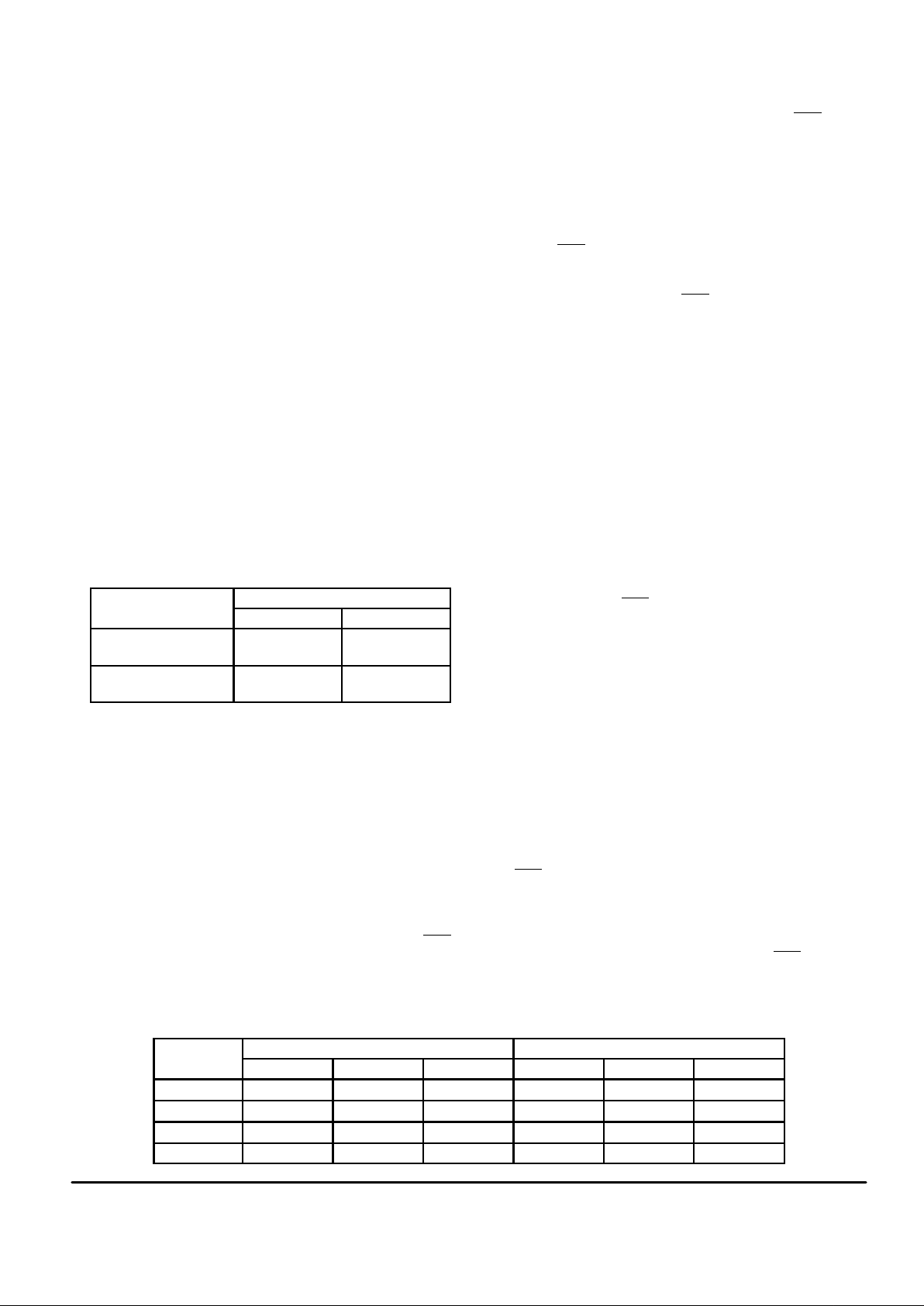
Table 1. Master Clock Frequency Determination
Master Clock Frequency Expected
BCLKR/CLKSEL
MC145554/64 MC145557/67
Clocked, 1, or Open 1.536 MHz
1.544 MHz
2.048 MHz
0 2.048 MHz 1.536 MHz
1.544 MHz
FRAME SYNCS AND DIGITAL I/O
These codec–filters can accommodate both of the industry
standard timing formats. The L ong Frame Sync mode is
used by Motorola’s MC145500 family of codec–filters and the
UDLT family of digital loop transceivers. The Short Frame
Sync mode is compatible with the IDL (Interchip Digital Link)
serial format used in Motorola’s ISDN family and by other
companies in their telecommunication devices. These
codec–filters use the length of the transmit frame sync (FSX)
to determine the timing format for both transmit and receive
unless t he part i s operating in the r eceive half–channel
mode.
In the Long Frame Sync mode, the frame sync pulses
must be at least three bit clock periods long. The DX and TS
X
outputs are enabled by the logical ANDing of F SX and
BCLKX; when both are high, the sign bit appears at the D
X
output. The next seven rising edges of BCLKX clock out the
remaining seven bits of the PCM word. The DX and TS
X
outputs return to a high impedance state on the falling edge of
the eighth bit clock or the falling edge of FSX, whichever
comes later. The receive PCM word is clocked into DR on the
eight falling BCLKR edges following an FSR rising edge.
For Short Frame Sync operation, the frame sync pulses
must be one bit clock period long. On the first BCLKX rising
edge after the falling edge of BCLKX has latched FSX high,
the DX and TS
X
outputs are enabled and the sign bit is presented on DX. The next seven rising edges of BCLKX clock
out the remaining seven bits of the PCM word; on the eighth
BCLKX falling edge, the DX and TS
X
outputs return to a high
impedance state. On the second falling BCLKR edge following an FSR rising edge, the receive sign bit is clocked into
DR. The next seven BCLKR falling edges clock in the remaining seven bits of the receive PCM word.
Table 2 shows the coding format of the transmit and re-
ceive PCM words.
HALF–CHANNEL MODES
In addition to the normal full–duplex operating mode, these
codec–filters can operate in both transmit and receive half–
channel modes. Transmit half–channel mode is entered by
holding FSR low. The VFRO output goes to analog ground
but remains in a low impedance state (to facilitate a hybrid
interface); PCM data at DR is ignored. Holding FSX low while
clocking FSR puts these devices in the receive half–channel
mode. In this state, the transmit input operational amplifier
continues to operate, but the rest of the transmit circuitry is
disabled; the DX and TS
X
outputs remain in a high impedance state. MCLKR is used as the internal master clock if it is
clocking. If MCLKR is not clocking, then MCLKX is used for
the internal master clock, but in that case it should be synchronous with FSR. If BCLKR is not clocking, BCLKX will be
used for the receive data, just as in the full–channel operating mode. In receive half–channel mode only, the length of
the FSR pulse is used to determine whether Short Frame
Sync or Long Frame Sync timing is used at DR.
POWER–DOWN
Holding both FSX and FSR low causes the part to go into
the power–down state. Power–down occurs approximately
2 ms after the last frame sync pulse is received. An alternative way to put these devices in power–down is to hold the
MCLKR/PDN pin high. When the chip is powered down, the
DX, TS
X
, and GSX outputs are high impedance, the VFRO,
VPO–, and VPO + operational amplifiers are biased with a
trickle current so that their respective outputs remain stable
at analog ground. To return the chip to the power–up state,
MCLKR/PDN must be low or clocking and at least one of the
frame sync pulses must be present. The DX and TS
X
outputs
will remain in a high–impedance state until the second FS
X
pulse after power–up.
Table 2. PCM Data Format
Mu–Law (MC145554/64) A–Law (MC145557/67)
Level
Sign Bit Chord Bits Step Bits Sign Bit Chord Bits Step Bits
+ Full Scale 1 0 0 0 0 0 0 0 1 0 1 0 1 0 1 0
+ Zero 1 1 1 1 1 1 1 1 1 1 0 1 0 1 0 1
– Zero 0 1 1 1 1 1 1 1 0 1 0 1 0 1 0 1
– Full Scale 0 0 0 0 0 0 0 0 0 0 1 0 1 0 1 0
MC145554•MC145557•MC145564•MC145567 MOTOROLA
6
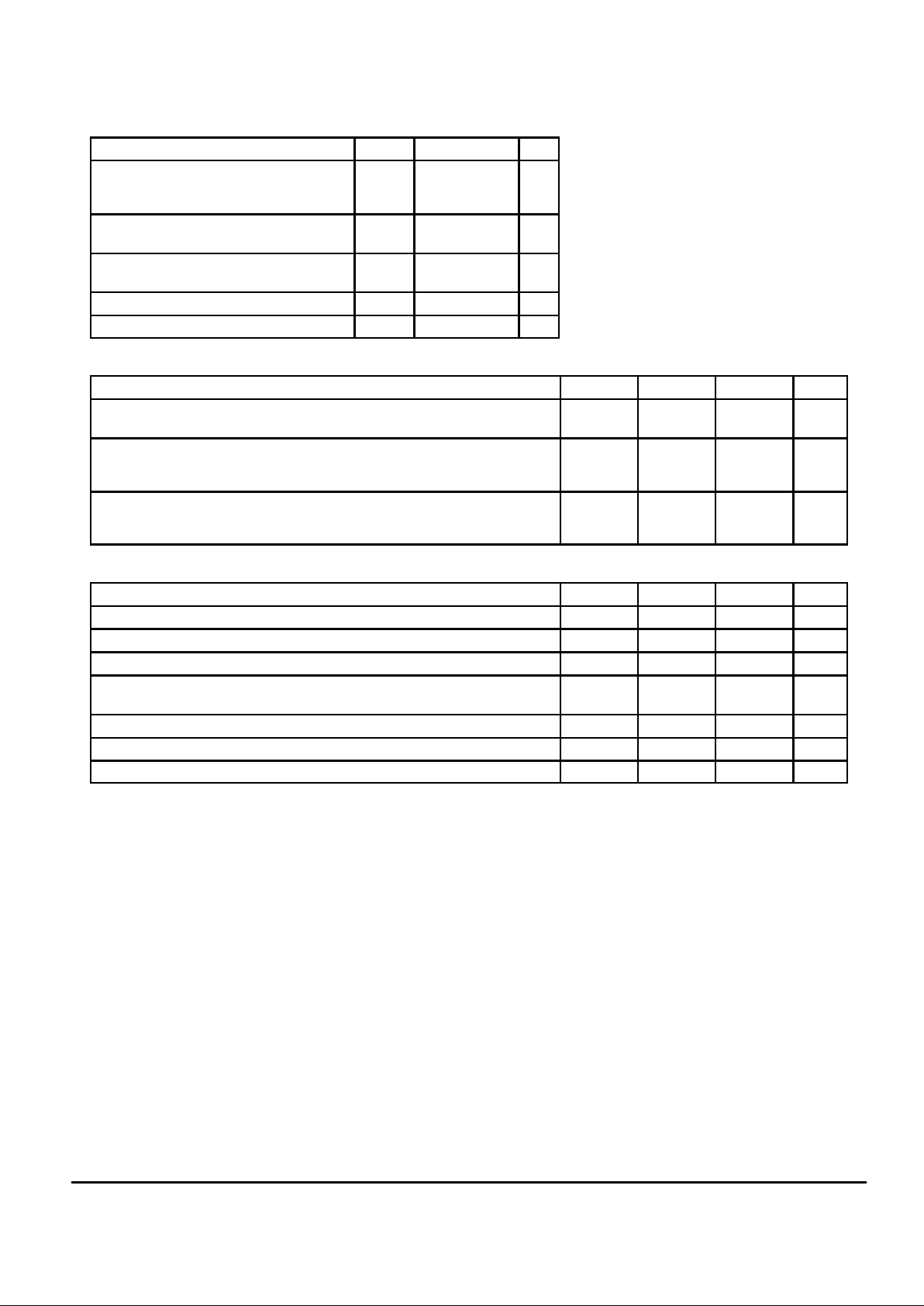
MAXIMUM RATINGS (Voltage Referenced to GNDA)
Rating
Symbol Value Unit
DC Supply Voltage VCC to V
BB
VCC to GNDA
VBB to GNDA
– 0.5 to + 13
– 0.3 to + 7.0
– 7.0 to + 0.3
V
Voltage on Any Analog Input or Output Pin VBB – 0.3 to
VCC + 0.3
V
Voltage on Any Digital Input or Output Pin GNDA – 0.3 to
VCC + 0.3
V
Operating Temperature Range T
A
– 40 to + 85 °C
Storage Temperature Range T
stg
– 85 to + 150 °C
POWER SUPPLY (T
A
= – 40 to + 85°C)
Characteristic
Min Typ Max Unit
DC Supply Voltage V
CC
V
BB
4.75
– 4.75
5.0
– 5.0
5.25
– 5.25
V
Active Power Dissipation (No Load) MC145554/57
MC145564/67
MC145564/67, VPI = V
BB
—
—
—
40
45
40
60
70
60
mW
Power–Down Dissipation (No Load) MC145554/57
MC145564/67
MC145564/67, VPI = V
BB
—
—
—
1.0
2.0
1.0
3.0
5.0
3.0
mW
DIGITAL LEVELS (V
CC
= 5 V ± 5%, VBB = – 5 V ± 5%, GNDA = 0 V, TA = – 40 to + 85°C)
Characteristic
Symbol Min Max Unit
Input Low Voltage V
IL
— 0.6 V
Input High Voltage V
IH
2.2 — V
Output Low Voltage DX or TSX, IOL = 3.2 mA V
OL
— 0.4 V
Output High Voltage DX, IOH = – 3.2 mA
IOH = – 1.6 mA
V
OH
2.4
VCC – 0.5
—
—
V
Input Low Current GNDA ≤ Vin ≤ V
CC
I
IL
– 10 + 10 µA
Input High Current GNDA ≤ Vin ≤ V
CC
I
IH
– 10 + 10 µA
Output Current in High Impedance State GNDA ≤ DX ≤ V
CC
I
OZ
– 10 + 10 µA
This device contains circuitry to protect
against damage due to high static voltages or
electric fields; however, it is advised that
normal precautions be taken to avoid application of any voltage higher than maximum
rated voltages to this high impedance circuit.
For proper operation it is recommended that
Vin and V
out
be constrained to the range V
SS
≤ (Vin or V
out
) ≤ VDD.
Unused inputs must always be tied to an
appropriate logic voltage level (e.g., VBB,
GNDA, or VCC).
 Loading...