

Motorola MC14553BCL, MC14553BCP, MC14553BDW Datasheet
MOTOROLA CMOS LOGIC DATA
1
MC14553B
The MC14553B 3–digit BCD counter consists of 3 negative edge triggered
BCD counters that are cascaded synchronously. A quad latch at the output
of each counter permits storage of any given count. The information is then
time division multiplexed, providing one BCD number or digit at a time. Digit
select outputs provide display control. All outputs are TTL compatible.
An on–chip oscillator provides the low–frequency scanning clock which
drives the multiplexer output selector.
This device is used in instrumentation counters, clock displays, digital
panel meters, and as a building block for general logic applications.
• TTL Compatible Outputs
• On–Chip Oscillator
• Cascadable
• Clock Disable Input
• Pulse Shaping Permits Very Slow Rise Times on Input Clock
• Output Latches
• Master Reset
MAXIMUM RATINGS* (Voltages Referenced to V
SS
)
Symbol
Parameter Value Unit
V
DD
DC Supply Voltage – 0.5 to + 18.0 V
Vin, V
out
Input or Output Voltage (DC or Transient) – 0.5 to VDD + 0.5 V
I
in
Input Current (DC or Transient), per Pin ± 10 mA
I
out
Output Current (DC or Transient), per Pin + 20 mA
P
D
Power Dissipation, per Package† 500 mW
T
stg
Storage Temperature – 65 to + 150
_
C
T
L
Lead Temperature (8–Second Soldering) 260
_
C
*Maximum Ratings are those values beyond which damage to the device may occur.
†Temperature Derating:
Plastic “P and D/DW” Packages: – 7.0 mW/_C From 65_C To 125_C
Ceramic “L” Packages: – 12 mW/_C From 100_C To 125_C
TRUTH TABLE
Inputs
Master
Reset
Clock Disable LE
Outputs
0 0 0 No Change
0 0 0 Advance
0 X 1 X No Change
0 1 0 Advance
0 1 0 No Change
0 0 X X No Change
0 X X Latched
0 X X 1 Latched
1 X X 0 Q0 = Q1 = Q2 = Q3 = 0
X = Don’t Care
SEMICONDUCTOR TECHNICAL DATA
Motorola, Inc. 1995
REV 3
1/94
BLOCK DIAGRAM
This device contains protection circuitry to
guard against damage due to high static
voltages or electric fields. However, precautions must be taken to avoid applications of
any voltage higher than maximum rated voltages to this high–impedance circuit. For proper
operation, Vin and V
out
should be constrained
to the range VSS v (Vin or V
out
) v VDD.
Unused inputs must always be tied to an
appropriate logic voltage level (e.g., either V
SS
or VDD). Unused outputs must be left open.
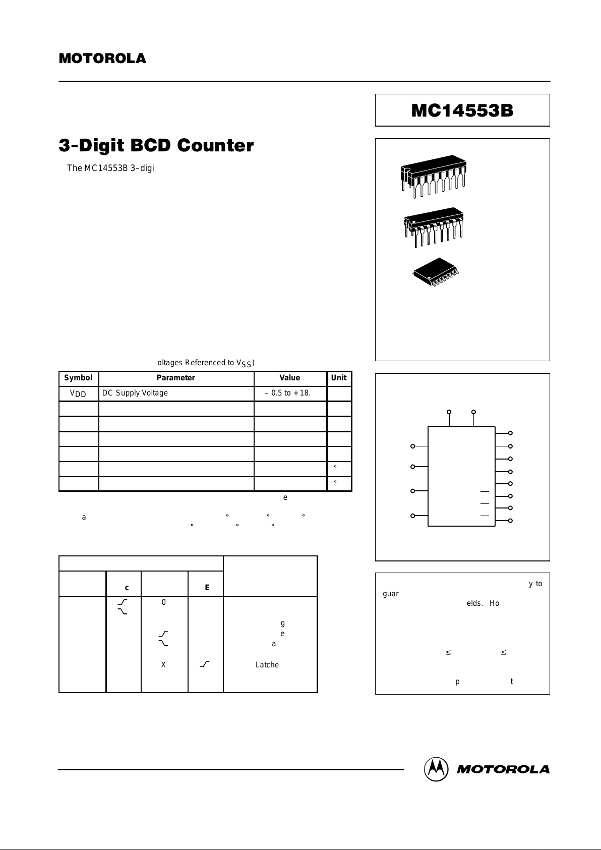
L SUFFIX
CERAMIC
CASE 620
ORDERING INFORMATION
MC14XXXBCP Plastic
MC14XXXBCL Ceramic
MC14XXXBDW SOIC
TA = – 55° to 125°C for all packages.
P SUFFIX
PLASTIC
CASE 648
DW SUFFIX
SOIC
CASE 751G
12
10
11
13
9
7
6
5
14
2
1
15
VDD = PIN 16
VSS = PIN 8
4 3
CLOCK
LE
DIS
MR
Q0
Q1
Q2
Q3
O.F.
DS
1
DS
2
DS
3
CIA CIB
MOTOROLA CMOS LOGIC DATAMC14553B
2
ELECTRICAL CHARACTERISTICS (Voltages Referenced to V
SS
)
V
– 55_C 25_C 125_C
Characteristic
Symbol
V
DD
Vdc
Min Max Min Typ # Max Min Max
Unit
Output Voltage “0” Level
Vin = VDD or 0
V
OL
5.0
10
15
—
—
—
0.05
0.05
0.05
—
—
—
0
0
0
0.05
0.05
0.05
—
—
—
0.05
0.05
0.05
Vdc
“1” Level
Vin = 0 or V
DD
V
OH
5.0
10
15
4.95
9.95
14.95
—
—
—
4.95
9.95
14.95
5.0
10
15
—
—
—
4.95
9.95
14.95
—
—
—
Vdc
Input Voltage “0” Level
(VO = 4.5 or 0.5 Vdc)
(VO = 9.0 or 1.0 Vdc)
(VO = 13.5 or 1.5 Vdc)
V
IL
5.0
10
15
—
—
—
1.5
3.0
4.0
—
—
—
2.25
4.50
6.75
1.5
3.0
4.0
—
—
—
1.5
3.0
4.0
Vdc
“1” Level
(VO = 0.5 or 4.5 Vdc)
(VO = 1.0 or 9.0 Vdc)
(VO = 1.5 or 13.5 Vdc)
V
IH
5.0
10
15
3.5
7.0
11
—
—
—
3.5
7.0
11
2.75
5.50
8.25
—
—
—
3.5
7.0
11
—
—
—
Vdc
Output Drive Current
(VOH = 4.6 Vdc) Source —
(VOH = 9.5 Vdc) Pin 3
(VOH = 13.5 Vdc)
I
OH
5.0
10
15
– 0.25
– 0.62
– 1.8
—
—
—
– 0.2
– 0.5
– 1.5
– 0.36
– 0.9
– 3.5
—
—
—
0.14
0.35
1.1
—
—
—
mAdc
(VOH = 4.6 Vdc) Source —
(VOH = 9.5 Vdc) Other
(VOH = 13.5 Vdc) Outputs
5.0
10
15
– 0.64
– 1.6
– 4.2
—
—
—
– 0.51
– 1.3
– 3.4
– 0.88
– 2.25
– 8.8
—
—
—
– 0.36
– 0.9
– 2.4
—
—
—
mAdc
(VOL = 0.4 Vdc) Sink —
(VOL = 0.5 Vdc) Pin 3
(VOL = 1.5 Vdc)
I
OL
5.0
10
15
0.5
1.1
1.8
—
—
—
0.4
0.9
1.5
0.88
2.25
8.8
—
—
—
0.28
0.65
1.20
—
—
—
mAdc
(VOL = 0.4 Vdc) Sink — Other
(VOL = 0.5 Vdc) Outputs
(VOL = 1.5 Vdc)
5.0
10
15
3.0
6.0
18
—
—
—
2.5
5.0
15
4.0
8.0
20
—
—
—
1.6
3.5
10
—
—
—
mAdc
Input Current I
in
15 — ±0.1 — ±0.00001 ±0.1 — ±1.0 µAdc
Input Capacitance
(Vin = 0)
C
in
— — — — 5.0 7.5 — — pF
Quiescent Current
(Per Package)
MR = V
DD
I
DD
5.0
10
15
—
—
—
5.0
10
20
—
—
—
0.010
0.020
0.030
5.0
10
20
—
—
—
150
300
600
µAdc
Total Supply Current**†
(Dynamic plus Quiescent,
Per Package)
(CL = 50 pF on all outputs, all
buffers switching)
I
T
5.0
10
15
IT = (0.35 µA/kHz) f + I
DD
IT = (0.85 µA/kHz) f + I
DD
IT = (1.50 µA/kHz) f + I
DD
µAdc
#Data labelled “Typ” is not to be used for design purposes but is intended as an indication of the IC’s potential performance.
**The formulas given are for the typical characteristics only at 25_C.
†To calculate total supply current at loads other than 50 pF:
IT(CL) = IT(50 pF) + (CL – 50) Vfk
where: IT is in µA (per package), CL in pF, V = (VDD – VSS) in volts, f in kHz is input frequency, and k = 0.004.
MOTOROLA CMOS LOGIC DATA
3
MC14553B
SWITCHING CHARACTERISTICS (C
L
= 50 pF, TA = 25_C)
Characteristic
Figure Symbol V
DD
Min Typ # Max Unit
Output Rise and Fall Time
t
TLH
, t
THL
= (1.5 ns/pF) CL + 25 ns
t
TLH
, t
THL
= (0.75 ns/pF) CL + 12.5 ns
t
TLH
, t
THL
= (0.55 ns/pF) CL + 9.5 ns
2a t
TLH
,
t
THL
5.0
10
15
—
—
—
100
50
40
200
100
80
ns
Clock to BCD Out 2a t
PLH
,
t
PHL
5.0
10
15
—
—
—
900
500
200
1800
1000
400
ns
Clock to Overflow 2a t
PHL
5.0
10
15
—
—
—
600
400
200
1200
800
400
ns
Reset to BCD Out 2b t
PHL
5.0
10
15
—
—
—
900
500
300
1800
1000
600
ns
Clock to Latch Enable Setup Time
Master Reset to Latch Enable Setup Time
2b t
su
5.0
10
15
600
400
200
300
200
100
—
—
—
ns
Removal Time
Latch Enable to Clock
2b t
rem
5.0
10
15
– 80
– 10
0
– 200
– 70
– 50
—
—
—
ns
Clock Pulse Width 2a t
WH(cl)
5.0
10
15
550
200
150
275
100
75
—
—
—
ns
Reset Pulse Width 2b t
WH(R)
5.0
10
15
1200
600
450
600
300
225
—
—
—
ns
Reset Removal Time — t
rem
5.0
10
15
– 80
0
20
– 180
– 50
– 30
—
—
—
ns
Input Clock Frequency 2a f
cl
5.0
10
15
—
—
—
1.5
5.0
7.0
0.9
2.5
3.5
MHz
Input Clock Rise Time 2b t
TLH
5.0
10
15
No
Limit
ns
Disable, MR, Latch Enable
Rise and Fall Times
— t
TLH
,
t
THL
5.0
10
15
—
—
—
—
—
—
15
5.0
4.0
µs
Scan Oscillator Frequency
(C1 measured in µF)
1 f
osc
5.0
10
15
—
—
—
1.5/C1
4.2/C1
7.0/C1
—
—
—
Hz
*The formulas given are for the typical characteristics only at 25_C.
#Data labelled “Typ” is not to be used for design purposes but is intended as an indication of the IC’s potential performance.
 Loading...