

MOTOROLA MC14551BCP, MC14551BD, MC14551BDR2, MC14551BF Datasheet
MC14551B
Quad 2-Channel Analog
Multiplexer/Demultiplexer
The MC14551B is a digitally–controlled analog switch. This device
implements a 4PDT solid state switch with low ON impedance and
very low OFF Leakage current. Control of analog signals up to the
complete supply voltage range can be achieved.
http://onsemi.com
• Triple Diode Protection on All Control Inputs
• Supply Voltage Range = 3.0 Vdc to 18 Vdc
• Analog Voltage Range (V
Note: VEE must be v V
– VEE) = 3.0 to 18 V
DD
SS
• Linearized Transfer Characteristics
• Low Noise — 12 nV√Cycle, f ≥ 1.0 kHz typical
• For Low R
CMOS Devices
, Use The HC4051, HC4052, or HC4053 High–Speed
ON
• Switch Function is Break Before Make
MAXIMUM RATINGS
Symbol Parameter Value Unit
V
Vin, V
T
2. Maximum Ratings are those values beyond which damage to the device
may occur.
3. Temperature Derating:
Plastic “P and D/DW” Packages: – 7.0 mW/_C From 65_C To 125_C
This device contains protection circuitry to guard against damage due to high
static voltages or electric fields. However, precautions must be taken to avoid
applications of any voltage higher than maximum rated voltages to this
high–impedance circuit. For proper operation, V
to the range V
V
DD
Unused inputs must always be tied to an appropriate logic voltage level (e.g.,
either V
DC Supply Voltage Range
DD
(Referenced to V
Input or Output Voltage (DC or
out
Transient) (Referenced to V
Control Input & V
I
Input Current (DC or Transient),
in
per Control Pin
I
Switch Through Current ± 25 mA
sw
P
Power Dissipation, per Package
D
T
Ambient Temperature Range – 55 to + 125
A
Storage Temperature Range – 65 to + 150
stg
T
Lead Temperature
L
(8–Second Soldering)
v (Vin or V
for Switch I/O.
SS
, VEE or VDD). Unused outputs must be left open.
SS
(2.)
, VSS ≥ VEE)
EE
for
SS
for Switch I/O)
EE
) v VDD for control inputs and VEE ≤ (Vin or V
out
– 0.5 to + 18.0 V
– 0.5 to VDD + 0.5 V
± 10 mA
(3.)
and V
in
500 mW
260
should be constrained
out
_
_
_
out
C
C
C
) ≤
MARKING
DIAGRAMS
16
PDIP–16
P SUFFIX
CASE 648
SOIC–16
D SUFFIX
CASE 751B
SOEIAJ–16
F SUFFIX
CASE 966
A = Assembly Location
WL or L = Wafer Lot
YY or Y = Year
WW or W = Work Week
MC14551BCP
AWLYYWW
1
16
14551B
AWLYWW
1
16
MC14551B
AWLYWW
1
ORDERING INFORMATION
Device Package Shipping
MC14551BCP PDIP–16 2000/Box
MC14551BD SOIC–16
MC14551BDR2 SOIC–16 2500/Tape & Reel
MC14551BF SOEIAJ–16 See Note 1.
1. For ordering information on the EIAJ version of
the SOIC packages, please contact your local
ON Semiconductor representative.
48/Rail
Semiconductor Components Industries, LLC, 2000
March, 2000 – Rev . 3
1 Publication Order Number:
MC14551B/D
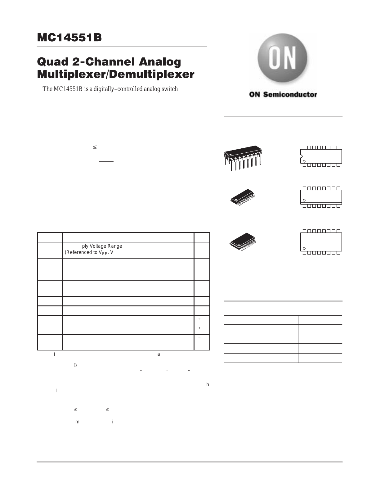
SWITCHES
IN/OUT
MC14551B
PIN ASSIGNMENT
1
V
V
W1
X0
X1
Y0
15
10
11
12
EE
SS
9
1
2
3
6
X
Y
2
3
4
6
7
8
CONTROL
W0
W1
X0
X1
Y0
Y1
Z0
Z1
16
15
14
13
125
11
10
9
W
X
Y
Z
V
DD
W0
W
Z
Z1
Z0
Y1
CONTROL
14
4
COMMONS
5
13
OUT/IN
VDD = Pin 16
V
= Pin 8
SS
V
= Pin 7
EE
Control ON
0 W0X0Y0Z0
1 W1X1Y1Z1
NOTE: Control Input referenced to V
Outputs reference to V
. VEE must be v VSS.
EE
, Analog Inputs and
SS
http://onsemi.com
2
MC14551B
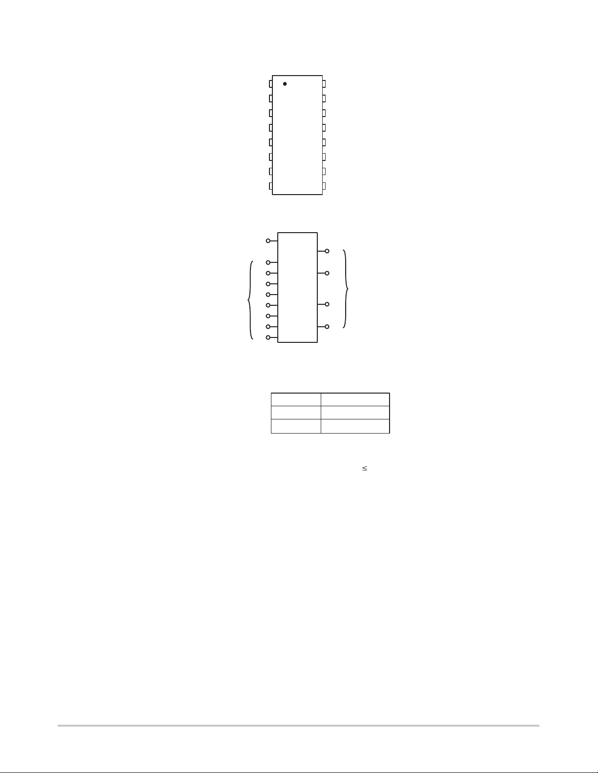
ELECTRICAL CHARACTERISTICS
– 55_C 25_C 125_C
Characteristic Symbol V
DD
Test Conditions
Min Max Min Typ
SUPPLY REQUIREMENTS (Voltages Referenced to VEE)
Power Supply Voltage
Range
Quiescent Current Per
Package
Total Supply Current
(Dynamic Plus
Quiescent, Per Package)
V
I
DD
I
D(AV)
DD
— VDD – 3.0 ≥ VSS ≥
V
EE
5.0
Control Inputs: V
10
VSS or VDD,
15
Switch I/O: V
v
VDD, and ∆V
v
500 mV
5.0
TA = 25_C only (The
10
channel component,
15
(V
in
– V
(5.)
)/Ron, is
out
EE
v V
in =
switch
3.0 18 3.0 — 18 3.0 18 V
—
5.0
10
20
—
—
—
I/O
—
—
Typical (0.20 µA/kHz) f + I
not included.)
CONTROL INPUT (Voltages Referenced to VSS)
Low–Level Input Voltage V
High–Level Input Voltage V
Input Leakage Current I
Input Capacitance C
5.0
IL
Ron = per spec,
10
I
off
= per spec
15
5.0
IH
Ron = per spec,
10
I
off
= per spec
15
in
15 Vin = 0 or V
— — — — 5.0 7.5 — — pF
in
DD
—
1.5
3.0
4.0
—
—
—
—
—
—
3.5
7.0
11
—
—
3.5
7.0
11
— ±0.1 — ±0.00001 ±0.1 — ±1.0 µA
SWITCHES IN/OUT AND COMMONS OUT/IN — W, X, Y, Z (Voltages Referenced to VEE)
Recommended Peak–to–
V
I/O
— Channel On or Off 0 V
0 — V
DD
Peak Voltage Into or Out
of the Switch
Recommended Static or
Dynamic Voltage Across
the Switch
(5.)
(Figure 3)
Output Offset Voltage V
ON Resistance R
∆ON Resistance Between
Any Two Channels
in the Same Package
Off–Channel Leakage
Current (Figure 8)
∆V
switch
∆R
I
OO
on
off
— Channel On 0 600 0 — 600 0 300 mV
— Vin = 0 V, No Load — — — 10 — — — µV
5.0
10
15
5.0
on
10
15
15 Vin = VIL or V
∆V
v 500 mV
switch
V
= VIL or V
in
(Control), and Vin =
0 to V
(Switch)
DD
(5.)
,
——800
IH
—
—
—
IH
— ±100 — ±0.05 ±100 — ±1000 nA
400
220
70
50
45
—
—
—
—
—
—
(Control) Channel to
Channel or Any One
Channel
Capacitance, Switch I/O C
Capacitance, Common O/I C
Capacitance, Feedthrough
(Channel Off)
I/O
O/I
C
I/O
— Switch Off — — — 10 — — — pF
— — — — 17 — — — pF
——Pins Not Adjacent
Pins Adjacent
—————
—
4. Data labeled “Typ” is not to be used for design purposes, but is intended as an indication of the IC’s potential performance.
5. For voltage drops across the switch (∆V
current out of the switch may contain both V
Maximum Ratings are exceeded. (See first page of this data sheet.)
) > 600 mV ( > 300 mV at high temperature), excessive VDD current may be drawn; i.e. the
switch
and switch input components. The reliability of the device will be unaffected unless the
DD
(4.)
Max Min Max
0.005
0.010
0.015
5.0
10
20
(0.07 µA/kHz) f + I
(0.36 µA/kHz) f + I
2.25
4.50
6.75
2.75
5.50
8.25
250
120
80
25
10
10
0.15
1.5
3.0
4.0
—
—
—
DD
1050
500
280
70
50
45
———
0.47
—
—
—
DD
DD
DD
—
—
—
3.5
7.0
11
0 V
—
—
—
—
—
—
—
150
300
600
1.5
3.0
4.0
—
—
—
DDVp–p
1200
520
300
135
95
65
—
—
Unit
µA
µA
V
V
Ω
Ω
pF
http://onsemi.com
3
MC14551B
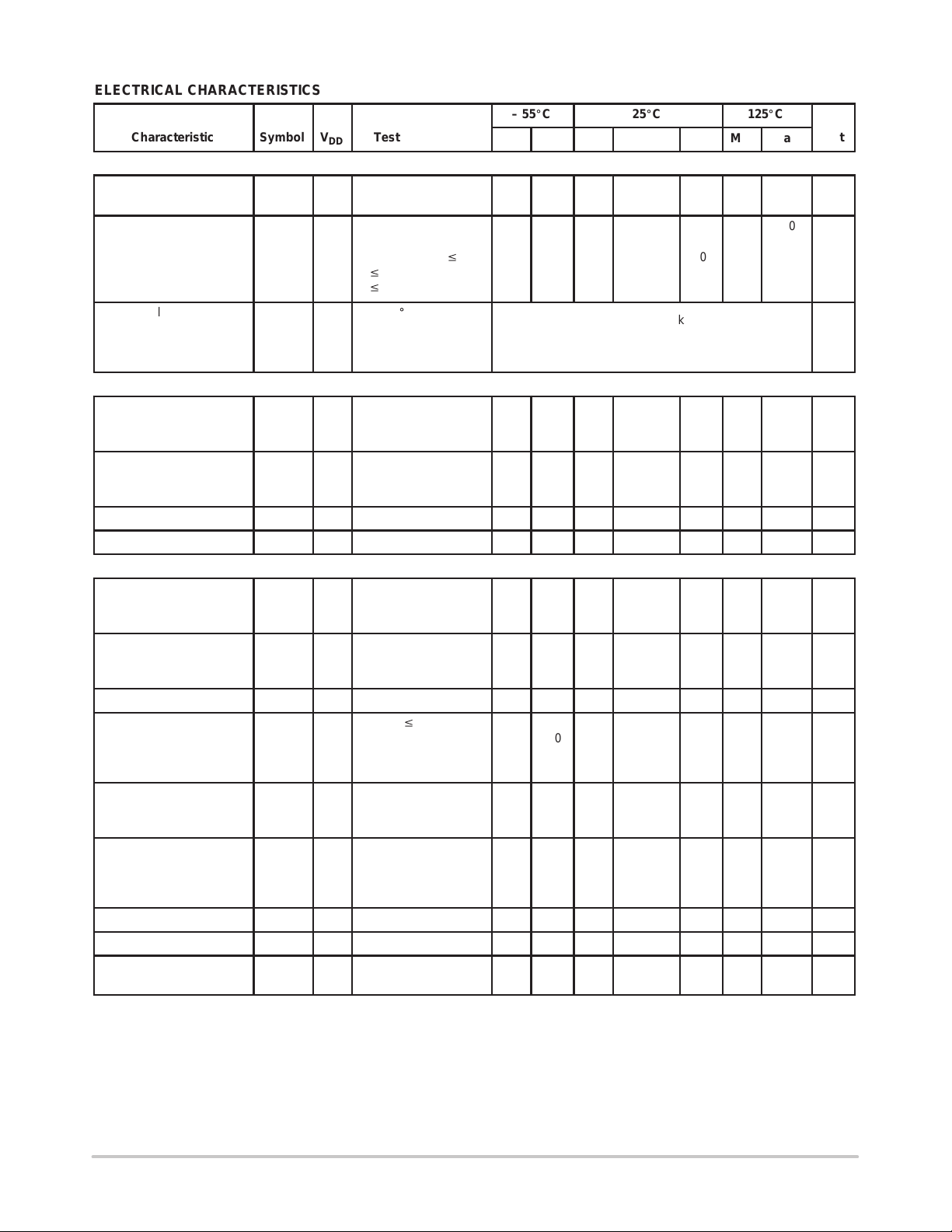
ELECTRICAL CHARACTERISTICS (C
Characteristic
Propagation Delay Times
Switch Input to Switch Output (R
, t
t
t
t
PLH
PLH
PLH
= (0.17 ns/pF) CL + 26.5 ns
PHL
, t
= (0.08 ns/pF) CL + 11 ns
PHL
, t
= (0.06 ns/pF) CL + 9.0 ns
PHL
Control Input to Output (RL = 10 kΩ)
V
= VSS (Figure 4)
EE
Second Harmonic Distortion
R
= 10 kΩ, f = 1 kHz, Vin = 5 V
L
Bandwidth (Figure 5)
R
= 1 kΩ, Vin = 1/2 (VDD – VEE)
L
20 Log (V
) = – 3 dB, CL = 50 pF
out/Vin
Off Channel Feedthrough Attenuation, Figure 5
R
= 1 kΩ, Vin = 1/2 (VDD – VEE)
L
f
= 55 MHz
in
Channel Separation (Figure 6)
R
= 1 kΩ, Vin = 1/2 (VDD – VEE)
L
= 3 MHz
f
in
Crosstalk, Control Input to Common O/I, Figure 7
R1 = 1 kΩ, R
Control t
= 10 kΩ,
L
= tf = 20 ns
r
L
p–p
= 50 pF, TA = 25_C, VEE v VSS)
L
Symbol
t
PLH
= 10 kΩ)
t
PLH
,
p–p
,
p–p
,
p–p
VDD – V
EE
Vdc
, t
PHL
5.0
10
15
, t
PHL
5.0
10
15
Min Typ
—
—
—
—
—
—
35
15
12
350
140
100
(6.)
Max Unit
90
40
30
875
350
250
— 10 — 0.07 — %
BW 10 — 17 — MHz
— 10 — – 50 — dB
— 10 — – 50 — dB
— 10 — 75 — mV
6. Data labelled “Typ” is not to be used for design purposes but is intended as an indication of the IC’s potential performance.
ns
ns
http://onsemi.com
4
 Loading...