

Motorola MC145484DW, MC145484SD Datasheet
SEMICONDUCTOR TECHNICAL DATA
Advance Information
The MC145484 is a general purpose per channel PCM Codec–Filter with pin
selectable Mu–Law or A–Law companding, and is offered in 20–pin SOG and
SSOP packages. This device performs the voice digitization and reconstruction
as well as the band limiting and smoothing required for PCM systems. This
device is designed to operate in both synchronous and asynchronous
applications and contains an on–chip precision reference voltage.
This device has an input operational amplifier whose output is the input to the
encoder section. The encoder section immediately low–pass filters the analog
signal with an active R–C filter to eliminate very high frequency noise from being
modulated down to the passband by the switched capacitor filter. From the
active R–C filter, the analog signal is converted to a dif ferential signal. From this
point, all analog signal processing is done differentially. This allows processing
of an analog signal that is twice the amplitude allowed by a single–ended
design, which reduces the significance of noise to both the inverted and
non–inverted signal paths. Another advantage of this differential design is that
noise injected via the power supplies is a common–mode signal that is
cancelled when the inverted and non–inverted signals are recombined. This
dramatically improves the power supply rejection ratio.
After the differential converter, a differential switched capacitor filter band–
passes the analog signal from 200 Hz to 3400 Hz before the signal is digitized
by the differential compressing A/D converter .
The decoder accepts PCM data and expands it using a differential D/A
converter. The output of the D/A is low–pass filtered at 3400 Hz and sinX/X
compensated by a differential switched capacitor filter. The signal is then filtered
by an active R–C filter to eliminate the out–of–band energy of the switched
capacitor filter.
The MC145484 PCM Codec–Filter has a high impedance V
reference pin
AG
which allows for decoupling of the internal circuitry that generates the
mid–supply V
reference voltage, to the VSS power supply ground. This
AG
reduces clock noise on the analog circuitry when external analog signals are
referenced to the power supply ground. This device is optimal for electronic
SLIC interfaces.
The MC145484 PCM Codec–Filter accepts a variety of clock formats,
including Short Frame Sync, Long Frame Sync, IDL, and GCI timing
environments. This device also maintains compatibility with Motorola’s family of
Telecommunication products, including the MC14LC5472 and MC145572
U–Interface Transceivers, MC145474/75 and MC145574 S/T–Interface Transceivers, MC145532 ADPCM Transcoder, MC145422/26 UDLT–1,
MC145421/25 UDL T–2, and MC3419/MC33120 SLICs.
The MC145484 PCM Codec–Filter utilizes CMOS due to its reliable
low–power performance and proven capability for complex analog/digital VLSI
functions.
• Single 5 V Power Supply
• Typical Power Dissipation of 15 mW, Power–Down of 0.01 mW
• Fully–Differential Analog Circuit Design for Lowest Noise
• Transmit Band–Pass and Receive Low–Pass Filters On–Chip
• Active R–C Pre–Filtering and Post–Filtering
• Mu–Law and A–Law Companding by Pin Selection
• On–Chip Precision Reference Voltage of 1.575 V for a – 0 dBm TLP @ 600 Ω
• Push–Pull 300 Ω Power Drivers with External Gain Adjust
• MC14LC5480EVK is the Evaluation Kit for This Device
This document contains information on a new product. Specifications and information herein are subject to change without notice.
REV 0
2/97 TN97022700
20
1
20
1
ORDERING INFORMATION
MC145484DW SOG Package
MC145484SD SSOP
PIN ASSIGNMENT
V
Ref
AG
RO–
PI
PO–
PO+ 5
V
DD
FSR
DR
BCLKR
PDI
Order this document
by MC145484/D
DW SUFFIX
SOG PACKAGE
CASE 751D
SD SUFFIX
SSOP
CASE 940C
1
2
3
4
6
7
8
9
10
20
19
18
17
16
15
14
13
12
11
V
AG
TI+
TI–
TG
Mu/A
V
SS
FST
DT
BCLKT
MCLK
Motorola, Inc. 1997
MC145484MOTOROLA
1
RO–
RECEIVE
SHIFT
FREQ
PI
DAC
REGISTER
DR
– 1
–
+
V
DD
R*
1
R*
V
SS
FREQ
PO–
PO+
V
DD
V
SS
Ref
V
AG
V
AG
TG
TI–
TI+
–
+
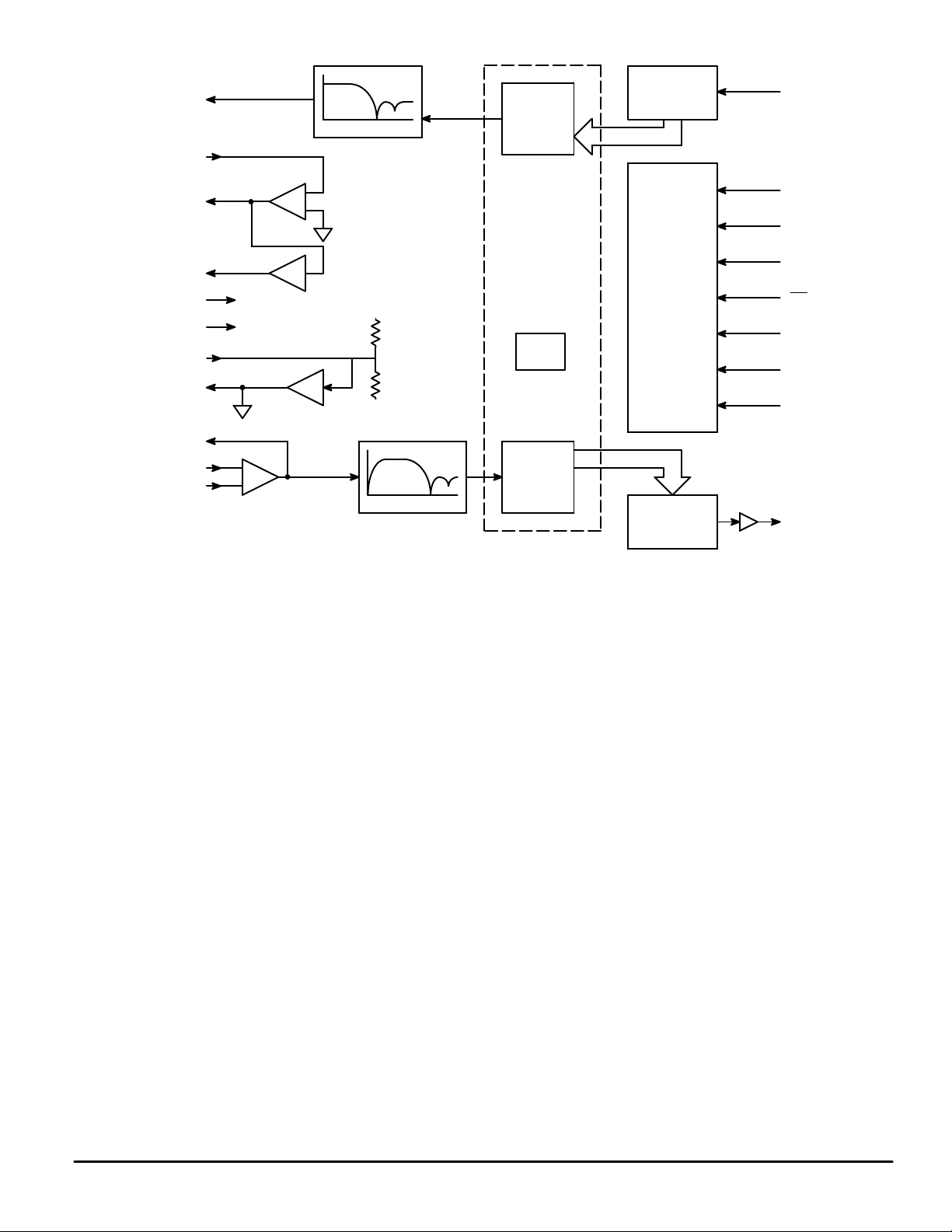
Figure 1. MC145484 5 V PCM Codec–Filter Block Diagram
DEVICE DESCRIPTION
A PCM Codec–Filter is used for digitizing and reconstructing the human voice. These devices are used primarily for
the telephone network to facilitate voice switching and transmission. Once the voice is digitized, it may be switched by
digital switching methods or transmitted long distance (T1,
microwave, satellites, etc.) without degradation. The name
codec is an acronym from ‘‘COder’’ for the analog–to–digital
converter (ADC) used to digitize voice, and ‘‘DECoder’’ for
the digital–to–analog converter (DAC) used for reconstructing voice. A codec is a single device that does both the ADC
and DAC conversions.
To digitize intelligible voice requires a signal–to–distortion
ratio of about 30 dB over a dynamic range of about 40 dB.
This may be accomplished with a linear 13–bit ADC and
DAC, but will far exceed the required signal–to–distortion
ratio at larger amplitudes than 40 dB below the peak amplitude. This excess performance is at the expense of data per
sample. Two methods of data reduction are implemented by
compressing the 13–bit linear scheme to companded
pseudo–logarithmic 8–bit schemes. The two companding
schemes are: Mu–255 Law, primarily in North America and
Japan; and A–Law, primarily used in Europe. These companding schemes are accepted world wide. These companding schemes follow a segmented or ‘‘piecewise–linear’’ curve
formatted as sign bit, three chord bits, and four step bits. For
a given chord, all sixteen of the steps have the same voltage
weighting. As the voltage of the analog input increases, the
four step bits increment and carry to the three chord bits
FSR
SHARED
DAC
SEQUENCE
AND
CONTROL
1.575 V
REF
ADC
TRANSMIT
SHIFT
REGISTER
BCLKR
Mu/A
PDI
MCLK
BCLKT
FST
DT
which increment. When the chord bits increment, the step
bits double their voltage weighting. This results in an effective resolution of six bits (sign + chord + four step bits) across
a 42 dB dynamic range (seven chords above 0, by 6 dB per
chord).
In a sampling environment, Nyquist theory says that to
properly sample a continuous signal, it must be sampled at a
frequency higher than twice the signal’s highest frequency
component. Voice contains spectral energy above 3 kHz, but
its absence is not detrimental to intelligibility. To reduce the
digital data rate, which is proportional to the sampling rate, a
sample rate of 8 kHz was adopted, consistent with a bandwidth of 3 kHz. This sampling requires a low–pass filter to
limit the high frequency energy above 3 kHz from distorting
the in–band signal. The telephone line is also subject to
50/60 Hz power line coupling, which must be attenuated
from the signal by a high–pass filter before the analog–to–
digital converter.
The digital–to–analog conversion process reconstructs a
staircase version of the desired in–band signal, which has
spectral images of the in–band signal modulated about the
sample frequency and its harmonics. These spectral images
are called aliasing components, which need to be attenuated
to obtain the desired signal. The low–pass filter used to attenuate these aliasing components is typically called a reconstruction or smoothing filter.
The MC145484 PCM Codec–Filter has the codec, both
presampling and reconstruction filters, and a precision voltage reference on–chip.
MC145484 MOTOROLA
2

PIN DESCRIPTIONS
POWER SUPPLY
V
DD
Positive Power Supply (Pin 6)
This is the most positive power supply and is typically con-
nected to + 5 V. This pin should be decoupled to V
0.1 µF ceramic capacitor.
V
SS
Negative Power Supply (Pin 15)
This is the most negative power supply and is typically
connected to 0 V.
V
AG
Analog Ground Output (Pin 20)
This output pin provides a mid–supply analog ground. This
pin should be decoupled to VSS with a 0.01 µF ceramic capacitor. All analog signal processing within this device is referenced to this pin. If the audio signals to be processed are
referenced to V
to avoid noise between V
, then special precautions must be utilized
SS
and the VAG pin. Refer to the ap-
SS
plications information in this document for more information.
The V
pin becomes high impedance when this device is in
AG
the powered–down mode.
Ref
V
AG
Analog Ground Reference Bypass (Pin 1)
This pin is used to capacitively bypass the on–chip circuitry that generates the mid–supply voltage for the V
pin. This pin should be bypassed to V
with a 0.1 µF ceram-
SS
ic capacitor using short, low inductance traces. The V
pin is only used for generating the reference voltage for the
pin. Nothing is to be connected to this pin in addition to
V
AG
the bypass capacitor. All analog signal processing within this
device is referenced to the V
processed are referenced to V
must be utilized to avoid noise between V
pin. If the audio signals to be
AG
, then special precautions
SS
and the VAG pin.
SS
Refer to the applications information in this document for
more information. When this device is in the powered–down
mode, the V
Ref pin is pulled to the VDD power supply with
AG
a non–linear, high–impedance circuit.
CONTROL
Mu/A
Mu/A Law Select (Pin 16)
This pin controls the compression for the encoder and the
expansion for the decoder. Mu–Law companding is selected
when this pin is connected to V
and A–Law companding is
DD
selected when this pin is connected to VSS.
PDI
Power–Down Input (Pin 10)
This pin puts the device into a low power dissipation mode
when a logic 0 is applied. When this device is powered down,
all of the clocks are gated off and all bias currents are turned
off, which causes RO–, PO–, PO+, TG, V
, and DT to be-
AG
SS
AG
with a
output
Ref
AG
come high impedance and the V
Ref pin is pulled to the
AG
VDD power supply with a non–linear, high–impedance circuit.
The device will operate normally when a logic 1 is applied to
this pin. The device goes through a power–up sequence
when this pin is taken to a logic 1 state, which prevents the
DT PCM output from going low impedance for at least two
FST cycles. The V
and VAG Ref circuits and the signal pro-
AG
cessing filters must settle out before the DT PCM output or
the RO– receive analog output will represent a valid analog
signal.
ANALOG INTERFACE
TI+
Transmit Analog Input (Non–Inverting) (Pin 19)
This is the non–inverting input of the transmit input gain
setting operational amplifier . This pin accommodates a differential to single–ended circuit for the input gain setting op
amp. This allows input signals that are referenced to the V
SS
pin to be level shifted to the VAG pin with minimum noise.
This pin may be connected to the V
pin for an inverting
AG
amplifier configuration if the input signal is already referenced to the V
pin. The common mode range of the TI+
AG
and TI– pins is from 1.2 V , to VDD minus 1.2 V . This is an FET
gate input.
The TI+ pin also serves as a digital input control for the
transmit input multiplexer. Connecting the TI+ pin to V
DD
will
place this amplifier’s output (TG) into a high–impedance
state, and selects the TG pin to serve as a high–impedance
input to the transmit filter. Connecting the TI+ pin to V
SS
will
also place this amplifier’s output (TG) into a high–impedance
state, and selects the TI– pin to serve as a high–impedance
input to the transmit filter.
TI–
Transmit Analog Input (Inverting) (Pin 18)
This is the inverting input of the transmit gain setting operational amplifier. Gain setting resistors are usually connected from this pin to TG and from this pin to the analog
signal source. The common mode range of the TI+ and TI–
pins is from 1.2 V to V
– 1.2 V. This is an FET gate input.
DD
The TI– pin also serves as one of the transmit input multiplexer pins when the TI+ pin is connected to V
is connected to V
, this pin is ignored. See the pin descrip-
DD
. When TI+
SS
tions for the TI+ and the TG pins for more information.
TG
Transmit Gain (Pin 17)
This is the output of the transmit gain setting operational
amplifier and the input to the transmit band–pass filter. This
op amp is capable of driving a 2 kΩ load. Connecting the TI+
pin to V
will place the TG pin into a high–impedance state,
DD
and selects the TG pin to serve as a high–impedance input to
the transmit filter. All signals at this pin are referenced to the
pin. When TI+ is connected to VSS, this pin is ignored.
V
AG
See the pin descriptions for the TI+ and TI– pins for more information. This pin is high impedance when the device is in
the powered–down mode.
MC145484MOTOROLA
3

RO–
Receive Analog Output (Inverting) (Pin 2)
This is the inverting output of the receive smoothing filter
from the digital–to–analog converter. This output is capable
of driving a 2 kΩ load to 1.575 V peak referenced to the V
AG
pin. If the device is operated half–channel with the FST pin
clocking and FSR pin held low, the receive filter input will be
conencted to the V
voltage. This minimizes transients at
AG
the RO– pin when full–channel operation is resumed by
clocking the FSR pin. This pin is high impedance when the
device is in the powered–down mode.
PI
Power Amplifier Input (Pin 3)
This is the inverting input to the PO– amplifier. The non–
inverting input to the PO– amplifier is internally tied to the
pin. The PI and PO – pins are used with external resis-
V
AG
tors in an inverting op amp gain circuit to set the gain of the
PO+ and PO– push–pull power amplifier outputs. Connecting PI to V
will power down the power driver amplifiers and
DD
the PO+ and PO– outputs will be high impedance.
PO–
Power Amplifier Output (Inverting) (Pin 4)
This is the inverting power amplifier output, which is used
to provide a feedback signal to the PI pin to set the gain of
the push–pull power amplifier outputs. This pin is capable of
driving a 300 Ω load to PO+. The PO+ and PO– outputs are
differential (push–pull) and capable of driving a 300 Ω load to
3.15 V peak, which is 6.3 V peak–to–peak. The bias voltage
and signal reference of this output is the V
pin. The V
AG
AG
pin cannot source or sink as much current as this pin, and
therefore low impedance loads must be between PO+ and
PO–. The PO+ and PO– differential drivers are also capable
of driving a 100 Ω resistive load or a 100 nF Piezoelectric
transducer in series with a 20 Ω resister with a small increase
in distortion. These drivers may be used to drive resistive
loads of ≥ 32 Ω when the gain of PO– is set to 1/4 or less.
Connecting PI to V
will power down the power driver am-
DD
plifiers and the PO+ and PO– outputs will be high impedance. This pin is also high impedance when the device is
powered down by the PDI
pin.
PO+
Power Amplifier Output (Non–Inverting) (Pin 5)
This is the non–inverting power amplifier output, which is
an inverted version of the signal at PO–. This pin is capable
of driving a 300 Ω load to PO–. Connecting PI to V
DD
will
power down the power driver amplifiers and the PO+ and
PO– outputs will be high impedance. This pin is also high impedance when the device is powered down by the PDI
pin.
See PI and PO– for more information.
DIGITAL INTERFACE
MCLK
Master Clock (Pin 11)
This is the master clock input pin. The clock signal applied
to this pin is used to generate the internal 256 kHz clock and
sequencing signals for the switched–capacitor filters, ADC,
and DAC. The internal prescaler logic compares the clock on
this pin to the clock at FST (8 kHz) and will automatically
accept 256, 512, 1536, 1544, 2048, 2560, or 4096 kHz. For
MCLK frequencies of 256 and 512 kHz, MCLK must be synchronous and approximately rising edge aligned to FST. For
optimum performance at frequencies of 1.536 MHz and
higher, MCLK should be synchronous and approximately rising edge aligned to the rising edge of FST. In many applications, MCLK may be tied to the BCLKT pin.
FST
Frame Sync, Transmit (Pin 14)
This pin accepts an 8 kHz clock that synchronizes the output of the serial PCM data at the DT pin. This input is compatible with various standards including IDL, Long Frame
Sync, Short Frame Sync, and GCI formats. If both FST and
FSR are held low for several 8 kHz frames, the device will
power down.
BCLKT
Bit Clock, Transmit (Pin 12)
This pin controls the transfer rate of transmit PCM data. In
the IDL and GCI modes it also controls the transfer rate of
the receive PCM data. This pin can accept any bit clock frequency from 64 to 4096 kHz for Long Frame Sync and Short
Frame Sync timing. This pin can accept clock frequencies
from 256 kHz to 4.096 MHz in IDL mode, and from 512 kHz
to 6.176 MHz for GCI timing mode.
DT
Data, Transmit (Pin 13)
This pin is controlled by FST and BCLKT and is high impedance except when outputting PCM data. When operating
in the IDL or GCI mode, data is output in either the B1 or B2
channel as selected by FSR. This pin is high impedance
when the device is in the powered down mode.
FSR
Frame Sync, Receive (Pin 7)
When used in the Long Frame Sync or Short Frame Sync
mode, this pin accepts an 8 kHz clock, which synchronizes
the input of the serial PCM data at the DR pin. FSR can be
asynchronous to FST in the Long Frame Sync or Short
Frame Sync modes. When an ISDN mode (IDL or GCI) has
been selected with BCLKR, this pin selects either B1 (logic 0)
or B2 (logic 1) as the active data channel.
BCLKR
Bit Clock, Receive (Pin 9)
When used in the Long Frame Sync or Short Frame Sync
mode, this pin accepts any bit clock frequency from 64 to
4096 kHz. When this pin is held at a logic 1, FST, BCLKT, DT,
and DR become IDL Interface compatible. When this pin is
held at a logic 0, FST , BCLKT, DT , and DR become GCI Interface compatible.
DR
Data, Receive (Pin 8)
This pin is the PCM data input, and when in a Long Frame
Sync or Short Frame Sync mode is controlled by FSR and
BCLKR. When in the IDL or GCI mode, this data transfer is
controlled by FST and BCLKT. FSR and BCLKR select the
B channel and ISDN mode, respectively .
MC145484 MOTOROLA
4

FUNCTIONAL DESCRIPTION
ANALOG INTERFACE AND SIGNAL PATH
The transmit portion of this device includes a low–noise,
three–terminal op amp capable of driving a 2 kΩ load. This
op amp has inputs of TI+ (Pin 19) and TI– (Pin 18) and its
output is TG (Pin 17). This op amp is intended to be configured in an inverting gain circuit. The analog signal may be
applied directly to the TG pin if this transmit op amp is independently powered down by connecting the TI+ input to the
power supply. The TG pin becomes high impedance
V
DD
when the transmit op amp is powered down. The TG pin is
internally connected to a 3–pole anti–aliasing pre–filter. This
pre–filter incorporates a 2–pole Butterworth active low–pass
filter, followed by a single passive pole. This pre–filter is followed by a single–ended to differential converter that is
clocked at 512 kHz. All subsequent analog processing utilizes fully–differential circuitry. The next section is a fully–differential, 5–pole switched–capacitor low–pass filter with a
3.4 kHz frequency cutoff. After this filter is a 3–pole
switched–capacitor high–pass filter having a cutoff frequency of about 200 Hz. This high–pass stage has a transmission zero at dc that eliminates any dc coming from the
analog input or from accumulated op amp offsets in the preceding filter stages. The last stage of the high–pass filter is
an autozeroed sample and hold amplifier.
One bandgap voltage reference generator and digital–to–
analog converter (DAC) are shared by the transmit and receive sections. The autozeroed, switched–capacitor
bandgap reference generates precise positive and negative
reference voltages that are virtually independent of temperature and power supply voltage. A binary–weighted capacitor
array (CDAC) forms the chords of the companding structure,
while a resistor string (RDAC) implements the linear steps
within each chord. The encode process uses the DAC, the
voltage reference, and a frame–by–frame autozeroed
comparator to implement a successive–approximation conversion algorithm. All of the analog circuitry involved in the
data conversion (the voltage reference, RDAC, CDAC, and
comparator) are implemented with a differential architecture.
The receive section includes the DAC described above, a
sample and hold amplifier, a 5–pole, 3400 Hz switched capacitor low–pass filter with sinX/X correction, and a 2–pole
active smoothing filter to reduce the spectral components of
the switched capacitor filter. The output of the smoothing filter is buffered by an amplifier , which is output at the RO– pin.
This output is capable of driving a 2 kΩ load to the V
The MC145484 also has a pair of power amplifiers that are
connected in a push–pull configuration. The PI pin is the inverting input to the PO– power amplifier. The non–inverting
input is internally tied to the V
pin. This allows this amplifier
AG
to be used in an inverting gain circuit with two external resis-
AG
pin.
tors. The PO+ a mplifier has a gain of minus one, and is internally connected to the PO– output. This complete power
amplifier circuit is a differential (push–pull) amplifier with adjustable gain that is capable of driving a 300 Ω load to
+ 12 dBm. The power amplifier may be powered down independently of the rest of the chip by connecting the PI pin to
.
V
DD
POWER–DOWN
There are two methods of putting this device into a low
power consumption mode, which makes the device nonfunctional and consumes virtually no power. PDI
is the power–
down input pin which, when taken low, powers down the
device. Another way to power the device down is to hold both
the FST and FSR pins low while the BCLKT and MCLK pins
are clocked. When the chip is powered down, the V
AG
, TG,
RO–, PO+, PO–, and DT outputs are high impedance and
Ref pin is pulled to the VDD power supply with a non–
the V
AG
linear, high–impedance circuit. To return the chip to the power–up state, PDI
must be high and the FST frame sync pulse
must be present while the BCLKT and MCLK pins are
clocked. The DT output will remain in a high–impedance
state for at least two 8 kHz FST pulses after power–up.
MASTER CLOCK
Since this codec–filter design has a single DAC architecture, the MCLK pin is used as the master clock for all analog
signal processing including analog–to–digital conversion,
digital–to–analog conversion, and for transmit and receive filtering functions of this device. The clock frequency applied to
the MCLK pin may be 256 kHz, 512 kHz, 1.536 MHz,
1.544 MHz, 2.048 MHz, 2.56 MHz, or 4.096 MHz. This device has a prescaler that automatically determines the proper
divide ratio to use for the MCLK input, which achieves the required 256 kHz internal sequencing clock. The clocking requirements of the MCLK input are independent of the PCM
data transfer mode (i.e., Long Frame Sync, Short Frame
Sync, IDL mode, or GCI mode).
DIGITAL I/O
The MC145484 is pin selectable for Mu–Law or A–Law.
Table 1 shows the 8–bit data word format for positive and
negative zero and full scale for both companding schemes.
Table 2 shows the series of eight PCM words for both Mu–
Law and A–Law that correspond to a digital milliwatt. The
digital mW is the 1 kHz calibration signal reconstructed by
the DAC that defines the absolute gain or 0 dBm0 Transmission Level Point (TLP) of the DAC. The timing for the PCM
data transfer is independent of the companding scheme selected. Refer to Figure 2 for a summary and comparison of
the four PCM data interface modes of this device.
MC145484MOTOROLA
5
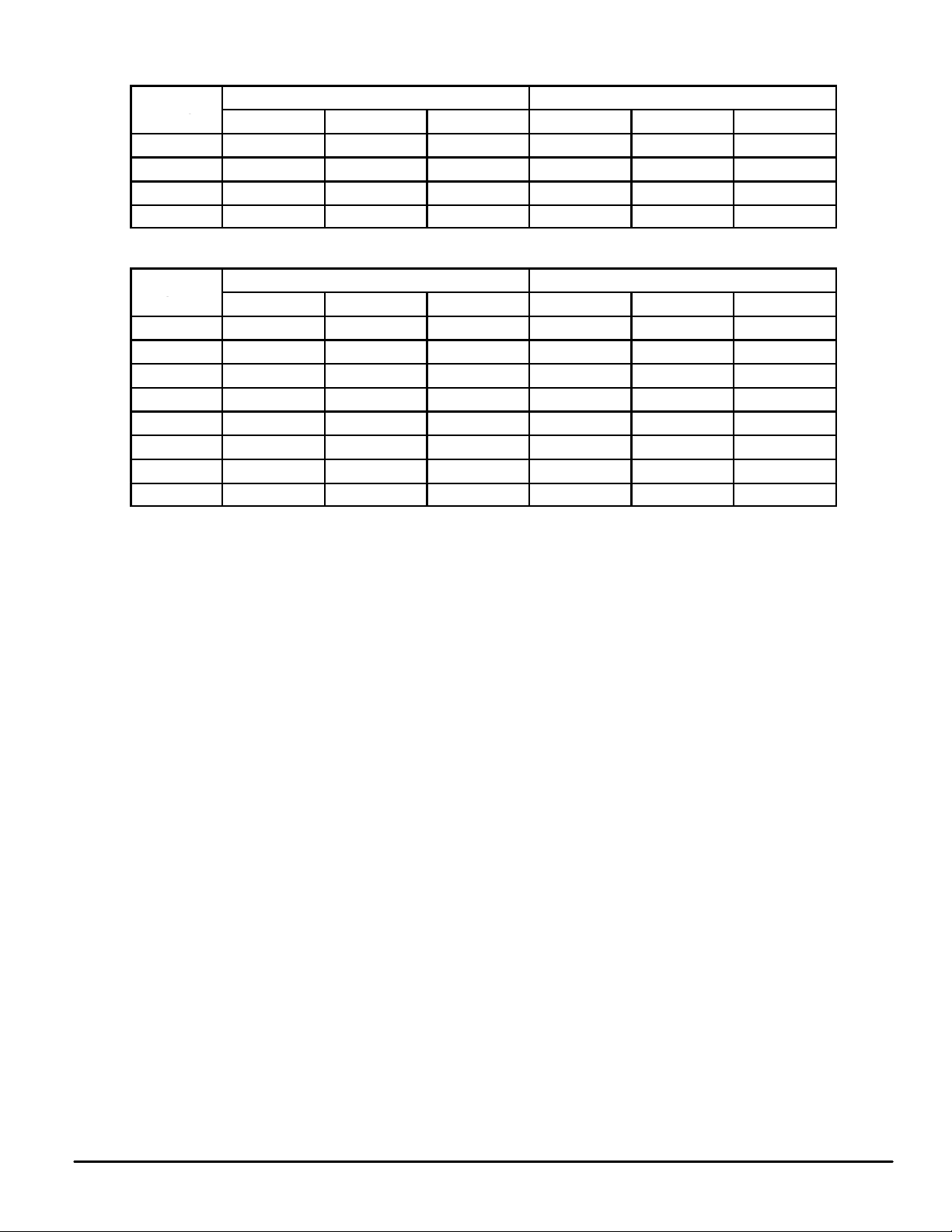
T able 1. PCM Codes for Zero and Full Scale
Mu–Law A–Law
Level
+ Full Scale 1 0 0 0 0 0 0 0 1 0 1 0 1 0 1 0
+ Zero 1 1 1 1 1 1 1 1 1 1 0 1 0 1 0 1
– Zero 0 1 1 1 1 1 1 1 0 1 0 1 0 1 0 1
– Full Scale 0 0 0 0 0 0 0 0 0 0 1 0 1 0 1 0
Sign Bit Chord Bits Step Bits Sign Bit Chord Bits Step Bits
Table 2. PCM Codes for Digital mW
Mu–Law A–Law
Phase
π/8 0 0 0 1 1 1 1 0 0 0 1 1 0 1 0 0
3π/8 0 0 0 0 1 0 1 1 0 0 1 0 0 0 0 1
5π/8 0 0 0 0 1 0 1 1 0 0 1 0 0 0 0 1
7π/8 0 0 0 1 1 1 1 0 0 0 1 1 0 1 0 0
9π/8 1 0 0 1 1 1 1 0 1 0 1 1 0 1 0 0
11π/8 1 0 0 0 1 0 1 1 1 0 1 0 0 0 0 1
13π/8 1 0 0 0 1 0 1 1 1 0 1 0 0 0 0 1
15π/8 1 0 0 1 1 1 1 0 1 0 1 1 0 1 0 0
Sign Bit Chord Bits Step Bits Sign Bit Chord Bits Step Bits
MC145484 MOTOROLA
6
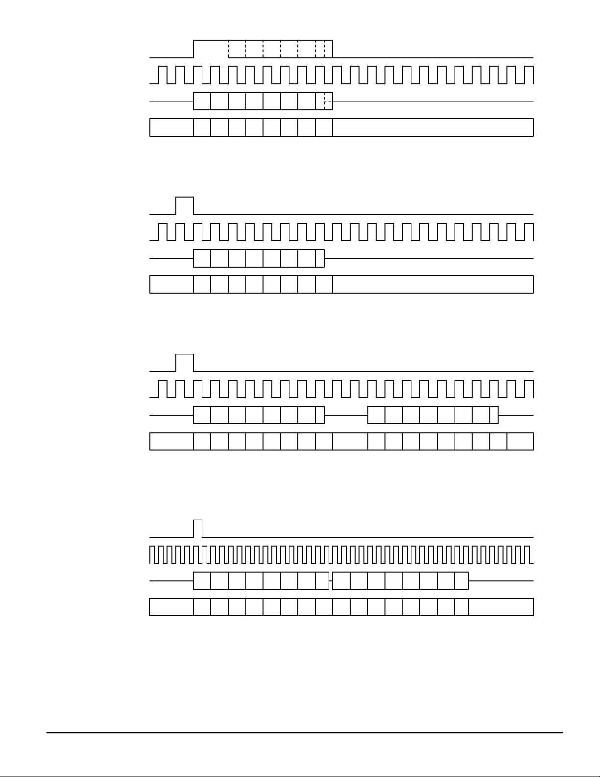
FST (FSR)
BCLKT (BCLKR)
DT
FST (FSR)
BCLKT (BCLKR)
DT
IDL SYNC (FST)
87654321
87654321DR DON’T CAREDON’T CARE
Figure 2a. Long Frame Sync (Transmit and Receive Have Individual Clocking)
87654321
8DR
7654321
DON’T CAREDON’T CARE
Figure 2b. Short Frame Sync (Transmit and Receive Have Individual Clocking)
IDL CLOCK (BCLKT)
IDL TX (DT)
IDL RX (DR)
Figure 2c. IDL Interface — BCLKR = 1 (Transmit and Receive Have Common Clocking)
FSC (FST)
DCL (BCLKT)
(DT)
D
out
Din (DR)
Figure 2d. GCI Interface — BCLKR = 0 (Transmit and Receive Have Common Clocking)
DON’T CARE
DON’T
CARE
87654321
DON’T
8
7654321 8
CARE
B2–CHANNEL (FSR = 1)B1–CHANNEL (FSR = 0)
87654321
87654321
B2–CHANNEL (FSR = 1)B1–CHANNEL (FSR = 0)
87654321
87654321
87654321
7654321
DON’T CARE
DON’T
CARE
Figure 2. Digital Timing Modes for the PCM Data Interface
MC145484MOTOROLA
7

Long Frame Sync
Long Frame Sync is the industry name for one type of
clocking format that controls the transfer of the PCM data
words. (Refer to Figure 2a.) The ‘‘Frame Sync’’ or ‘‘Enable’’ is
used for two specific synchronizing functions. The first is to
synchronize the PCM data word transfer, and the second is
to control the internal analog–to–digital and digital–to–analog
conversions. The term ‘‘Sync’’ refers to the function of synchronizing the PCM data word onto or off of the multiplexed
serial PCM data bus, which is also known as a PCM highway. The term ‘‘Long’’ comes from the duration of the frame
sync measured in PCM data clock cycles. Long Frame Sync
timing occurs when the frame sync is used directly as the
PCM data output driver enable. This results in the PCM output going low impedance with the rising edge of the transmit
frame sync, and remaining low impedance for the duration of
the transmit frame sync.
The implementation of Long Frame Sync has maintained
compatibility and been optimized for external clocking simplicity . This optimization includes the PCM data output going
low impedance with the logical AND of the transmit frame
sync (FST) with the transmit data bit clock (BCLKT). The optimization also includes the PCM data output (DT) remaining
low impedance until the middle of the LSB (seven and a half
PCM data clock cycles) or until the FST pin is taken low,
whichever occurs last. This requires the frame sync to be
approximately rising edge aligned with the initiation of the
PCM data word transfer, but the frame sync does not have a
precise timing requirement for the end of the PCM data word
transfer. The device recognizes Long Frame Sync clocking
when the frame sync is held high for two consecutive falling
edges of the transmit data clock. The transmit logic decides
on each frame sync whether it should interpret the next
frame sync pulse as a Long or a Short Frame Sync. This decision is used for receive circuitry also. The device is designed to prevent PCM bus contention by not allowing the
PCM data output to go low impedance for at least two frame
sync cycles after power is applied or when coming out of the
powered down mode.
The receive side of the device is designed to accept the
same frame sync and data clock as the transmit side and to
be able to latch its own transmit PCM data word. Thus the
PCM digital switch needs to be able to generate only one
type of frame sync for use by both transmit and receive sections of the device.
The logical AND of the receive frame sync with the receive
data clock tells the device to start latching the 8–bit serial
word into the receive data input on the falling edges of the
receive data clock. The internal receive logic counts the receive data clock cycles and transfers the PCM data word to
the digital–to–analog converter sequencer on the ninth data
clock rising edge.
This device is compatible with four digital interface modes.
To ensure that this device does not reprogram itself for a different timing mode, the BCLKR pin must change logic state
no less than every 125 µs. The minimum PCM data bit clock
frequency of 64 kHz satisfies this requirement.
Short Frame Sync
Short Frame Sync is the industry name for the type of
clocking format that controls the transfer of the PCM data
words (refer to Figure 2b). The ‘‘Frame Sync’’ or ‘‘Enable’’ is
used for two specific synchronizing functions. The first is to
synchronize the PCM data word transfer, and the second is
to control the internal analog–to–digital and digital–to–analog
conversions. The term ‘‘Sync’’ refers to the function of synchronizing the PCM data word onto or off of the multiplexed
serial PCM data bus, which is also known as a PCM highway. The term ‘‘Short’’ comes from the duration of the frame
sync measured in PCM data clock cycles. Short Frame Sync
timing occurs when the frame sync is used as a ‘‘pre–synchronization’’ pulse that is used to tell the internal logic to
clock out the PCM data word under complete control of the
data clock. The Short Frame Sync is held high for one falling
data clock edge. The device outputs the PCM data word beginning with the following rising edge of the data clock. This
results in the PCM output going low impedance with the rising edge of the transmit data clock, and remaining low impedance until the middle of the LSB (seven and a half PCM
data clock cycles).
The device recognizes Short Frame Sync clocking when
the frame sync is held high for one and only one falling edge
of the transmit data clock. The transmit logic decides on each
frame sync whether it should interpret the next frame sync
pulse as a Long or a Short Frame Sync. This decision is used
for receive circuitry also. The device is designed to prevent
PCM bus contention by not allowing the PCM data output to
go low impedance for at least two frame sync cycles after
power is applied or when coming out of the powered down
mode.
The receive side of the device is designed to accept the
same frame sync and data clock as the transmit side and to
be able to latch its own transmit PCM data word. Thus the
PCM digital switch needs to be able to generate only one
type of frame sync for use by both transmit and receive sections of the device.
The falling edge of the receive data clock latching a high
logic level at the receive frame sync input tells the device to
start latching the 8–bit serial word into the receive data input
on the following eight falling edges of the receive data clock.
The internal receive logic counts the receive data clock
cycles and transfers the PCM data word to the digital–to–
analog converter sequencer on the rising data clock edge after the LSB has been latched into the device.
This device is compatible with four digital interface modes.
To ensure that this device does not reprogram itself for a different timing mode, the BCLKR pin must change logic state
no less than every 125 µs. The minimum PCM data bit clock
frequency of 64 kHz satisfies this requirement.
Interchip Digital Link (IDL)
The Interchip Digital Link (IDL) Interface is one of two
standard synchronous 2B+D ISDN timing interface modes
with which this device is compatible. In the IDL mode, the device can communicate in either of the two 64 kbps B channels (refer to Figure 2c for sample timing). The IDL mode is
selected when the BCLKR pin is held high for two or more
FST (IDL SYNC) rising edges. The digital pins that control
the transmit and receive PCM word transfers are reprogrammed to accommodate this mode. The pins affected are
FST , FSR, BCLKT, DT , and DR. The IDL Interface consists of
four pins: IDL SYNC (FST), IDL CLK (BCLKT), IDL TX (DT),
and IDL RX (DR). The IDL interface mode provides access to
both the transmit and receive PCM data words with common
control clocks of IDL Sync and IDL Clock. In this mode, the
MC145484 MOTOROLA
8
 Loading...