

Page 1
Freescale Semiconductor, Inc.
19
查询"MC145181"供应商
" %
"$ $! % #!
Order this document by MC145181/D
nc...
I
cale Semiconductor,
Frees
! "!
The MC145181 is a dual frequency synthesizer containing very–low
supply voltage circuitry. The device supports two independent loops with a
single input reference and operates down to 1.8 V. Phase noise reduction
circuitry is incorporated into the device.
The MC145181 operates up to 550 MHz on the main loop and up to
60 MHz on the secondary loop. The device has a 32/33 prescaler for the
main loop. Lock detection circuitry for both loops is multiplexed to a single
output.
Two 8–bit DACs are powered through a dedicated pin. The DAC supply
range is 1.8 to 3.6 V; this voltage may differ from the main supply.
An on–chip voltage multiplier supplies power to the phase/frequency
detectors. Thus, in a 2 V application, the detectors are supplied with 4 V
power. In 2.6 to 3.6 V applications, the multiplied voltage is regulated at
approximately 5 V . The current source/sink phase/frequency detector for the
main loop is designed to achieve faster lock times than a conventional
detector. Both high and low current outputs are available along with a timer,
double buffers, and a MOSFET switch to adjust the external low–pass filter
response.
There are several levels of standby which are controllable with a 1–byte
transfer through the serial port. Either of the PLLs and/or the reference
oscillator may be independently placed in the low–power standby state. In
addition, any of the phase/frequency detector outputs may be placed in the
floating state to facilitate modulation of the external VCOs. Either DAC may
be placed in standby via a 4–byte transfer.
The MC145181 facilitates designing the receiver’s first and second local
oscillators for ReFLEX two–way paging applications. Also, the device
accommodates generation of the transmit carrier.
• Operating Frequency
Main Loop: 100 to 550 MHz
Secondary Loop: 10 to 60 MHz
• Operating Supply Voltage: 1.8 to 3.6 V
• Nominal Supply Current, Both Loops Active: 3 mA
• Maximum Standby Current, All Systems Shut Down: 10 µA
• Phase Detector Output Current:
1.8 V Supply — PD
w
2.5 V Supply — PD
• Two Independent 8–Bit DACs with Separate Supply Pin (Up to 3.6 V)
• Lock Detect Output with Adjustable Lock Indication Window
• Independent R Counters Allow Independent Step Sizes for Each Loop
• Main Loop Divider Range: 992 to 262,143
• Secondary Loop Divider Range: 7 to 8,191
• Fractional Reference Counters Divider Range: 20 to 32,767.5
• Auxiliary Reference Divider with Small–Signal Differential
Output — Ratios: 8, 10, 12.5
• Three General–Purpose Outputs
• Direct Interface to Motorola SPI Data Port Up to 10 Mbps
–Hi: 2.8 mA, PD
out
–Hi: 4.4 mA, PD
out
–Lo: 0.7 mA
out
–Lo: 1.1 mA
out
BiCMOS COMPONENT
FOR 2 OR 3 VOLT
SYSTEMS
SEMICONDUCTOR
TECHNICAL DATA
32 1
(Scale 2:1)
PLASTIC PACKAGE
(LQFP–32, Tape & Reel Only)
VERY–SMALL 5 x 5 mm BODY
DEVELOPMENT SYSTEM
The MC145230EVK, which contains hardware and
software, is strongly recommended for system
development. (The user must provide the VCOs for
evaluating the MC145181.) The software supports
all features and modes of operation of the device. Up
to four boards or devices can be controlled and the
user is alerted to error conditions. The control
program may be used with any board based on the
MC145181, MC145225, or MC145230.
ORDERING INFORMATION
Device
MC145181FTAR2 550/60 MHz LQFP–32
CASE 873C
Main/Secondary
Loop
Maximum
Frequency
Package
ReFLEX and BitGrabber are trademarks of Motorola, Inc.
are subject to change without notice.
MOTOROLA RF/IF DEVICE DATA
For More Information On This Product,
Go to: www.freescale.com
Motorola, Inc. 1999 Rev 1This document contains information on a new product. Specifications and information herein
1
Page 2

Freescale Semiconductor, Inc.
MC145181
查询"MC145181"供应商
CONTENTS
1. BLOCK DIAGRAM 3. . . . . . . . . . . . . . . . . . . . . . . . . . . . . . . . . . . . . . . . . . . . . . . . . . . . .
2. PIN CONNECTIONS 4. . . . . . . . . . . . . . . . . . . . . . . . . . . . . . . . . . . . . . . . . . . . . . . . . . . .
3. PARAMETER TABLES 4. . . . . . . . . . . . . . . . . . . . . . . . . . . . . . . . . . . . . . . . . . . . . . . . . .
3A. Maximum Ratings 4. . . . . . . . . . . . . . . . . . . . . . . . . . . . . . . . . . . . . . . . . . . . . . . . .
3B. DC Electrical Characteristics 5. . . . . . . . . . . . . . . . . . . . . . . . . . . . . . . . . . . . . . . .
3C. PD
3D. PD
3E. DAC Characteristics 6. . . . . . . . . . . . . . . . . . . . . . . . . . . . . . . . . . . . . . . . . . . . . . .
3F. Voltage Multiplier and Keep–alive Oscillator Characteristics 6. . . . . . . . . . . . .
3G. Dynamic Characteristics of Digital Pins 6. . . . . . . . . . . . . . . . . . . . . . . . . . . . . . .
3H. Dynamic Characteristics of Loop and f
4. DEVICE OVERVIEW 9. . . . . . . . . . . . . . . . . . . . . . . . . . . . . . . . . . . . . . . . . . . . . . . . . . . .
4A. Serial Interface and Registers 9. . . . . . . . . . . . . . . . . . . . . . . . . . . . . . . . . . . . . . .
4B. Reference Input and Counters Circuits 9. . . . . . . . . . . . . . . . . . . . . . . . . . . . . . . .
4C. Loop Divider Inputs and Counter Circuits 9. . . . . . . . . . . . . . . . . . . . . . . . . . . . . .
nc...
I
4D. Voltage Multiplier and Keep–alive Circuits 9. . . . . . . . . . . . . . . . . . . . . . . . . . . . .
4E. Phase/Frequency Detectors 10. . . . . . . . . . . . . . . . . . . . . . . . . . . . . . . . . . . . . . . . .
4F. Lock Detectors 10. . . . . . . . . . . . . . . . . . . . . . . . . . . . . . . . . . . . . . . . . . . . . . . . . . . .
4G. DACs 10. . . . . . . . . . . . . . . . . . . . . . . . . . . . . . . . . . . . . . . . . . . . . . . . . . . . . . . . . . . .
4H. General–purpose Outputs 10. . . . . . . . . . . . . . . . . . . . . . . . . . . . . . . . . . . . . . . . . .
–Hi and PD
out
i
Phase/Frequency Detector Characteristics 5. . . . . . . . . . . . . . . . . . . . .
out
–Lo Phase/Frequency Detector Characteristics 5. . . . . .
out
Pins 8. . . . . . . . . . . . . . . . . . . . . . . . .
out
cale Semiconductor,
Frees
5. PIN DESCRIPTIONS 11. . . . . . . . . . . . . . . . . . . . . . . . . . . . . . . . . . . . . . . . . . . . . . . . . . . .
5A. Digital Pins 11. . . . . . . . . . . . . . . . . . . . . . . . . . . . . . . . . . . . . . . . . . . . . . . . . . . . . . .
5B. Reference Pins 13. . . . . . . . . . . . . . . . . . . . . . . . . . . . . . . . . . . . . . . . . . . . . . . . . . . .
5C. Loop Pins 13. . . . . . . . . . . . . . . . . . . . . . . . . . . . . . . . . . . . . . . . . . . . . . . . . . . . . . . .
5D. Analog Outputs 14. . . . . . . . . . . . . . . . . . . . . . . . . . . . . . . . . . . . . . . . . . . . . . . . . . . .
5E. External Components 15. . . . . . . . . . . . . . . . . . . . . . . . . . . . . . . . . . . . . . . . . . . . . .
5F. Supply Pins 15. . . . . . . . . . . . . . . . . . . . . . . . . . . . . . . . . . . . . . . . . . . . . . . . . . . . . . .
6. DETAILED REGISTER DESCRIPTIONS 16. . . . . . . . . . . . . . . . . . . . . . . . . . . . . . . . . . .
6A. C Register 16. . . . . . . . . . . . . . . . . . . . . . . . . . . . . . . . . . . . . . . . . . . . . . . . . . . . . . . .
6B. Hr Register 19. . . . . . . . . . . . . . . . . . . . . . . . . . . . . . . . . . . . . . . . . . . . . . . . . . . . . . .
6C. N Register 20. . . . . . . . . . . . . . . . . . . . . . . . . . . . . . . . . . . . . . . . . . . . . . . . . . . . . . . .
6D. Ri Register 22. . . . . . . . . . . . . . . . . . . . . . . . . . . . . . . . . . . . . . . . . . . . . . . . . . . . . . .
6E. Hni Register 25. . . . . . . . . . . . . . . . . . . . . . . . . . . . . . . . . . . . . . . . . . . . . . . . . . . . . .
6F. D Register 26. . . . . . . . . . . . . . . . . . . . . . . . . . . . . . . . . . . . . . . . . . . . . . . . . . . . . . . .
7. APPLICATIONS INFORMATION 29. . . . . . . . . . . . . . . . . . . . . . . . . . . . . . . . . . . . . . . . .
7A. Crystal Oscillator Considerations 29. . . . . . . . . . . . . . . . . . . . . . . . . . . . . . . . . . . .
7B. Main Loop Filter Design — Conventional 34. . . . . . . . . . . . . . . . . . . . . . . . . . . . . .
7C. Main Loop Filter Design — Adapt 41. . . . . . . . . . . . . . . . . . . . . . . . . . . . . . . . . . . .
7D. Secondary Loop Filter Design 50. . . . . . . . . . . . . . . . . . . . . . . . . . . . . . . . . . . . . . .
7E. Voltage Multiplier Stall Avoidance 57. . . . . . . . . . . . . . . . . . . . . . . . . . . . . . . . . . . .
8. PROGRAMMER’S GUIDE 58. . . . . . . . . . . . . . . . . . . . . . . . . . . . . . . . . . . . . . . . . . . . . . .
8A. Quick Reference 58. . . . . . . . . . . . . . . . . . . . . . . . . . . . . . . . . . . . . . . . . . . . . . . . . .
8B. Initializing the Device 65. . . . . . . . . . . . . . . . . . . . . . . . . . . . . . . . . . . . . . . . . . . . . . .
8C. Programming Without Adapt 66. . . . . . . . . . . . . . . . . . . . . . . . . . . . . . . . . . . . . . . .
8D. Programming Utilizing Horseshoe With Adapt 66. . . . . . . . . . . . . . . . . . . . . . . . . .
8E. Controlling the DACs 67. . . . . . . . . . . . . . . . . . . . . . . . . . . . . . . . . . . . . . . . . . . . . . .
9. APPLICATION CIRCUIT 69. . . . . . . . . . . . . . . . . . . . . . . . . . . . . . . . . . . . . . . . . . . . . . . . .
10. OUTLINE DIMENSIONS 70. . . . . . . . . . . . . . . . . . . . . . . . . . . . . . . . . . . . . . . . . . . . . . . . .
2
For More Information On This Product,
Go to: www.freescale.com
MOTOROLA RF/IF DEVICE DATA
Page 3
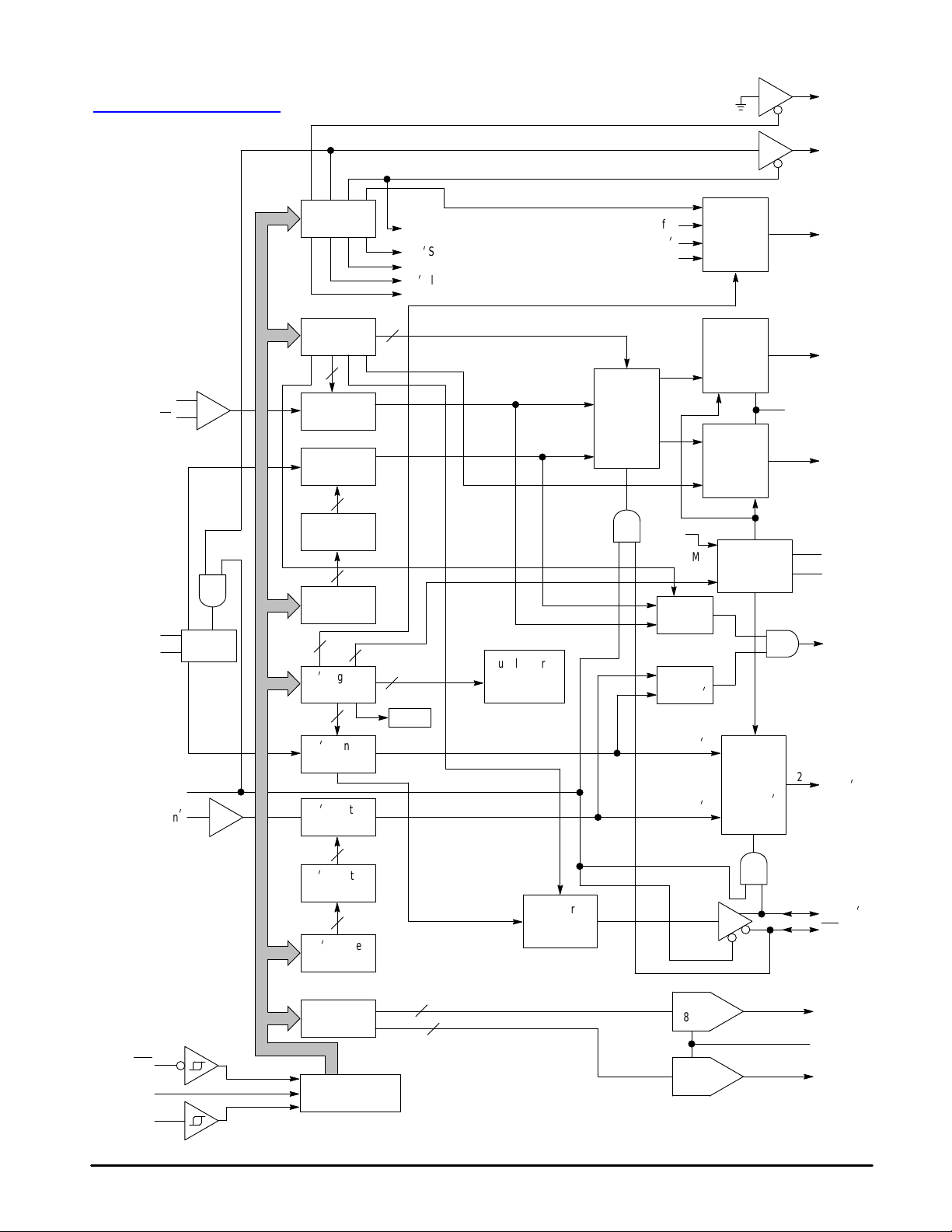
1. BLOCK DIAGRAM
查询"MC145181"供应商
Freescale Semiconductor, Inc.
MC145181
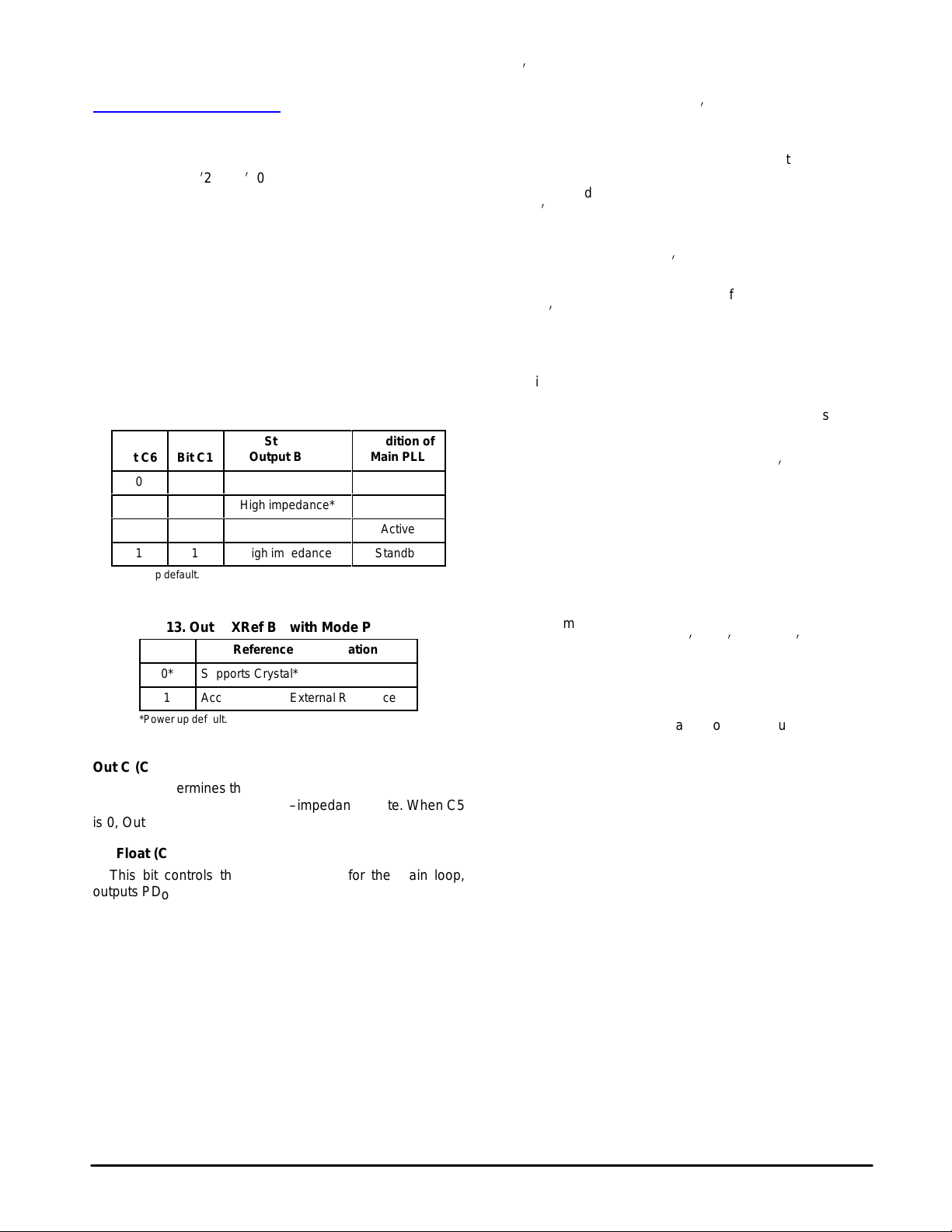
Out C
Out B/Ref
PLL Stby
16
25
Output C
Output B
nc...
I
cale Semiconductor,
Frees
Osc
Osc
f
in
f
in
1
e
32
b
Mode
f
12
13
Oscillator
30
i
in
f
Polarity
Out A
f
R
i
R
Function
Osc
V–Mult
Control
Lock
Detector
Lock
Detector
fRi
fVi
Output A
Mux
High–
current
Charge
Pump
Low–
current
Charge
Pump
Voltage
Multiplier
and Regulator
i
Phase/
Frequency
Detector
17
Rx
i
Polarity
i
9
19
20
23
28
27
Output A
PD
PD
21
C
22
C
8
LD
PD
f
out
f
out
out
out
mult
reg
out
/Pol
/Pol
–Hi
–Lo
i
i
C Register
8 Bits
N Register
24 Bits
18
+
–
Amp
10
Amp
N Counter
18 Stages
R Counter
16 Stages
16
R Register
16 Bits
16
Hr Register
16 Bits
2
Ri Register
24 Bits
16
Ri Counter
16 Stages
Ni Counter
13 Stages
13
Ni Register
13 Bits
13 MSBs
Hni Register
16 Bits
3
3
2
T est
PLL Stby
PLL
i
Stby
PD Float
PDi Float
Osc Stby
Lo–I Gain
Window
Supply Current
Minimization
Circuit
Ratio
Auxiliary
Divider
3 Stages
f
f
Timer
V
R
Ph Det Pulse
Phase/
Frequency
Detector,
Timer,
and Control
5
Enb
6
D
in
7
Clk
MOTOROLA RF/IF DEVICE DATA
D Register
16 Bits
Shift Register and
Address Generator
8
8
Power Connections:
Pin 2 = DAC V
Pins 11, 24, 26, and 29 = V
Pins 14, 15, 18, and 31 = Gnd
pos
pos
For More Information On This Product,
Go to: www.freescale.com
DAC
8 Bits
DAC
8 Bits
3
DAC1
2
DAC V
pos
4
DAC2
3
Page 4
2. PIN CONNECTIONS
Freescale Semiconductor, Inc.
MC145181
查询"MC145181"供应商
V
fin′
Gnd
Osc
b
Osc
1
e
DAC V
nc...
I
pos
DAC1
DAC2
Enb
D
in
Clk
LD
2
3
4
5
6
7
8
10
9
Mode
Output
A
This device contains 15,260 active transistors.
V
11
pos
pos
12
f
in
f
out
Pol
13
f
f
/
out
′
Pol
14
Gnd
in
Output
/
pos
15
Gnd
BV
2532 31 30 29 28 27 26
16
Output
C
24
23
22
21
20
19
18
17
V
pos
PD
C
reg
C
mult
PD
PD
Gnd
Rx
out
out
out
′
–Lo
–Hi
cale Semiconductor,
Frees
3. PARAMETER TABLES
3A. MAXIMUM RATINGS (Voltages Referenced to Gnd, unless otherwise stated)
Parameter Symbol Value Unit
DC Supply Voltages V
DC Input Voltage — Osce, fin, fini
Din, Clk, Enb
DC Output Voltage V
DC Input Current, per Pin I
DC Output Current, per Pin I
DC Supply Current, V
Power Dissipation, per Package P
Storage Temperature T
Lead Temperature, 1 mm from Case for
10 Seconds
NOTES:1. Maximum Ratings are those values beyond which damage to the device may occur.
, f
/Poli, f
out
pos
Functional operation should be restricted to the limits in the Electrical Characteristics tables
or Pin Descriptions section.
2. ESD (electrostatic discharge) immunity meets Human Body Model (HBM) up to 2000 V.
Additional ESD data available upon request.
, Mode,
/Pol
out
and Gnd Pins I 25 mA
pos
DAC V
V
out
out
stg
T
,
pos
in
in
D
L
–0.5 to 3.6 V
–0.5 to V
–0.5 to V
–65 to 150 °C
+ 0.5 V
pos
+ 0.5 V
pos
±10 mA
±20 mA
100 mW
260 °C
This device contains protection circuitry to
guard against damage due to high static voltages or electric fields. However, precautions
must be taken to avoid applications of any
voltage higher than maximum rated voltages
to this high–impedance circuit.
4
For More Information On This Product,
Go to: www.freescale.com
MOTOROLA RF/IF DEVICE DATA
Page 5
nc...
I
cale Semiconductor,
Frees
Freescale Semiconductor, Inc.
MC145181
3B. DC ELECTRICAL CHARACTERISTICS
V
= 1.8 to 3.6 V, Voltages Referenced to Gnd, TA = –40 to 85°C, unless otherwise statedtt
pos
查询"MC145181"供应商
Parameter
Maximum Low–Level Input Voltage
Minimum High–Level Input Voltage
Minimum Hysteresis Voltage (Clk) V
Maximum Low–Level Output Voltage
Minimum High–Level Output Voltage
Minimum Low–Level Output Current
Minimum High–Level Output Current
Minimum Low–Level Output Current (Output C) V
Maximum Input Leakage Current
Maximum Output Leakage Current
Maximum ON Resistance (Output C) 1.8 V ≤ V
Maximum Standby Supply Current
NOTES:1. For supply voltages restricted to 2.5 to 2.9 V and an ambient temperature range of –10 to 60°C, Output C has a guaranteed ON resistance range of 23
3C. PD
Maximum Source Current Variation Part–to–Part (See Note) V
Maximum Sink–versus–Source Mismatch (See Note) V
Output Voltage Range (See Note) I
Maximum Three–State Leakage Current V
NOTE: Percentages calculated using the following formula: (Maximum Value – Minimum Value)/Maximum Value.
(Din, Clk, Enb, Mode, f
(Din, Clk, Enb
(Din, Clk, Enb
(V
to 44 Ω.
2. The total supply current drain for the keep–alive oscillator, voltage multiplier, and regulator is approximately 250 µA.
3. When the Mode pin is tied high, bit C6 must be programmed to a 0 for minimum supply current drain. Otherwise, if C6 = 1, the current drain is approximately
8 µA for a 1.8 V supply and approximately 40 µA for a 3.6 V supply. This restriction on bit C6 does not apply when the Mode pin is tied low.
4. To ensure minimum standby supply current drain, the voltage potential at the C
See discussion in Section 5E under C
–Hi AND PD
out
Nominal Output Current, V
Nominal Output Current, V
Rx = 2.0 kΩ, Voltages Referenced to Gnd, Voltage Multiplier ON, TA = –40 to 85°C
and DAC V
pos
, Mode, f
(LD, Output A, Output B)
(LD, Output A, Output B)
(LD, Output A, Output B)
(LD, Output A, Output B)
, Mode, f
out
Parameter
/Poli, f
out
out
out
(Output B, Output C)
pos
out
/Poli, f
out
/Poli, f
out
Tied Together)
.
mult
–Lo PHASE/FREQUENCY DETECTOR CHARACTERISTICS
= 1.8 V: PD
pos
≥ 2.5 V: PD
pos
f
/Poli and f
out
/Pol)
f
/Poli and f
out
/Pol)
I
= 20 µA V
out
I
= –20 µA V
out
V
= 0.3 V I
out
V
= V
out
pos
= 0.2 V I
out
Vin = V
/Pol)
–Hi = 2.8 mA, PD
out
–Hi = 4.4 mA, PD
out
pos
Configured as Inputs
V
= V
out
State
2.5 V ≤ V
Vin = V
Standby Mode; Oscillator in Standby Mode;
DAC1 and DAC2 Output = Zero; Keep–alive
Oscillator Off (Notes 2, 3, and 4)
pos
pos
pos
pos
Condition Symbol
/Pol Configured as Inputs
out
/Pol Configured as Inputs
out
– 0.3 V I
or Gnd; f
or Gnd; Output in High–Impedance
< 2.5 V Supply
≤ 3.6 V Supply (Note 1)
or Gnd; Outputs Open; Both PLLs in
out
out
/Poli and f
out
pin must not be allowed to fall below the potential at the V
mult
–Lo = 0.7 or 0.35 mA
–Lo = 1.1 or 0.55 mA
Condition
= 0.5 x V
out
= 0.5 x V
out
Variation ≤ 27% 0.6 to V
out
= 0 or V
out
Cmult
Cmult
Cmult
out
/Pol
V
V
Hys
OL
OH
OL
I
I
OZ
R
I
STBY
Guaranteed
Limit
0.3 x V
IL
IH
OL
OH
in
on
0.7 x V
V
pos
Guaranteed
Limit
±14 %
20 %
– 0.6 V V
Cmult
±50 nA
Unit
pos
V
V
Ω
pins.
Unit
pos
pos
100 mV
0.1 V
– 0.1 V
0.7 mA
–0.7 mA
2.8 mA
±1.0 µA
±1 µA
75
50
10 µA
3D. PD
Minimum Low–Level Output Current V
Minimum High–Level Output Current V
Maximum Three–State Leakage Current V
i
PHASE/FREQUENCY DETECTOR CHARACTERISTICS
out
V
= 1.8 to 3.6 V , Voltages Referenced to Gnd, Voltage Multiplier ON, TA = –40 to 85°C
pos
Parameter
MOTOROLA RF/IF DEVICE DATA
For More Information On This Product,
Go to: www.freescale.com
Guaranteed
Condition
= 0.3 V 0.3 mA
out
= V
out
= 0 or V
out
– 0.3 V –0.3 mA
Cmult
Cmult
Limit
±50 nA
Unit
5
Page 6
Á
Á
Á
Á
Á
Á
Á
Á
Á
Á
Á
Á
Freescale Semiconductor, Inc.
MC145181
3E. DAC CHARACTERISTICS
V
= 1.8 to 3.6 V, DAC V
pos
查询"MC145181"供应商
Parameter
Resolution
Maximum Integral Nonlinearity
Maximum Offset Voltage from Gnd
Maximum Offset V oltage from DAC V
Maximum Output Impedance
ББББББББББББ
Maximum Standby Current
Maximum Supply Current per DAC @ DAC V
= 1.8 to 3.6 V; TA = –40 to 85°C
pos
No External Load
pos
pos
No External Load
Over Entire Output Range, Including Zero
БББББББББББ
Output (which is Low–power Standby)
Zero Output, No External Load
pin
Except with Zero Output, No External Load
Condition
Guaranteed
Limit
8
±1
1
2
STBY
(DAC V
130
in Section 3B)
) / 36
pos
ББББББ
(See I
Unit
Bits
LSB
LSB
LSB
kΩ
Á
mA
3F. VOLTAGE MULTIPLIER AND KEEP–ALIVE OSCILLATOR CHARACTERISTICS
Voltages Referenced to Gnd, TA = –40 to 85°C
Guaranteed
nc...
I
Voltage Multiplier Output Voltage
ББББББББББББ
ББББББББББББ
Keep–alive Refresh Frequency
Parameter
5 MHz Refresh Rate, 100 µA Continuous
Sourcing, Measured at C
БББББББББББ
V
= 1.8 V
pos
V
= 3.6 V
БББББББББББ
pos
V
= 1.8 to 3.6 V
pos
Condition
mult
pin
ББББББ
ББББББ
Limit
3.32 to 3.78
4.75 to 5.35
300 to 700
Unit
Á
V
Á
kHz
cale Semiconductor,
Frees
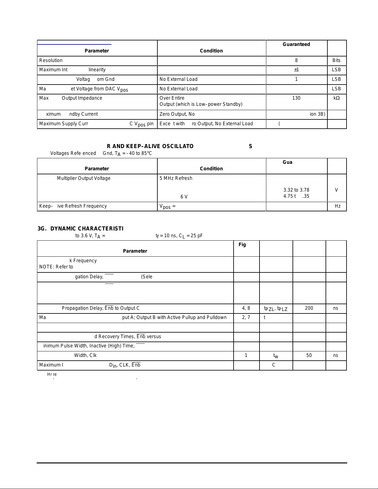
3G. DYNAMIC CHARACTERISTICS OF DIGITAL PINS
V
= 1.8 to 3.6 V, TA = –40 to 85°C, Input tr = tf = 10 ns, CL = 25 pF
pos
Figure
Parameter
Serial Data Clk Frequency
NOTE: Refer to Clk tw Below
Maximum Propagation Delay, Enb to Output A (Selected as General–Purpose Output) 2, 7 t
Maximum Propagation Delay, Enb to Output B 2, 3, 7, 8 t
Maximum Propagation Delay, Enb to Output C 4, 8 t
Maximum Output Transition T ime, Output A; Output B with Active Pullup and Pulldown 2, 7 t
Minimum Setup and Hold Times, Din versus Clk 5 tsu, t
Minimum Setup, Hold, and Recovery Times, Enb versus Clk 6 tsu, th, t
Minimum Pulse Width, Inactive (High) Time, Enb 6 t
Minimum Pulse Width, Clk 1 t
Maximum Input Capacitance — Din, CLK, Enb C
*For Hr register access, the minimum limit is 20 Osce cycles.
For Hni register access, the minimum limit is 27 fini
For N register access, the minimum limit is 20 Osce cycles + 99 fin cycles.
When the timer is used for adapt, the minimum limit after the second N register access and before the next register access is the time–out interval + 99 fin cycles.
cycles.
No.
1 f
t
t
Symbol
clk
PLH
, t
PLH
, t
PZL
PZH
PZL
TLH
, t
, t
, t
, t
w
w
in
PHL
PHL
PLZ
PHZ
PLZ
THL
h
rec
Guaranteed
Limit
dc to 10 MHz
200 ns
,
200 ns
,
200 ns
75 ns
30 ns
100 ns
* cycles
50 ns
10 pF
Unit
6
For More Information On This Product,
Go to: www.freescale.com
MOTOROLA RF/IF DEVICE DATA
Page 7
Freescale Semiconductor, Inc.
MC145181
nc...
I
cale Semiconductor,
Frees
查询"MC145181"供应商
90%
Clk
50%
10%
Enb
Output B
Output B
Output B
Output B
D
in
Clk
Figure 1. Figure 2.
t
f
t
w
Figure 3.
t
PZL
t
PLZ
t
PZH
t
PHZ
Figure 5. Figure 6.
Valid
50%
t
su
1/f
clk
50%
50%
t
r
10%
90%
t
h
t
w
90%
10%
V
pos
Gnd
V
pos
Gnd
V
pos
Gnd
V
pos
Gnd
Enb
Clk
Enb
Output A
Output B
Enb
Output C
Output C
50%
t
50%
First
Clock
su
10%
50%
t
PLH
90%
t
TLH
Figure 4.
t
PZL
t
PLZ
t
h
Last
Clock
50%
90%
10%
t
PHL
t
THL
V
pos
Gnd
High
Impedance
High
Impedance
t
w
t
rec
V
pos
Gnd
V
Gnd
V
Gnd
pos
pos
Figure 7. Figure 8.
Device
Under
Test
*Includes all probe and fixture capacitance.
MOTOROLA RF/IF DEVICE DATA
Test Point
CL*
Device
Under
Test
*Includes all probe and fixture capacitance.
For More Information On This Product,
Go to: www.freescale.com
Test Point
CL*
Source current and
limit voltage to V
for t
and t
PLZ
Sink current and
limit voltage to Gnd
for t
and t
PHZ
250 µA
PZL
PZH
pos
.
.
7
Page 8
Freescale Semiconductor, Inc.
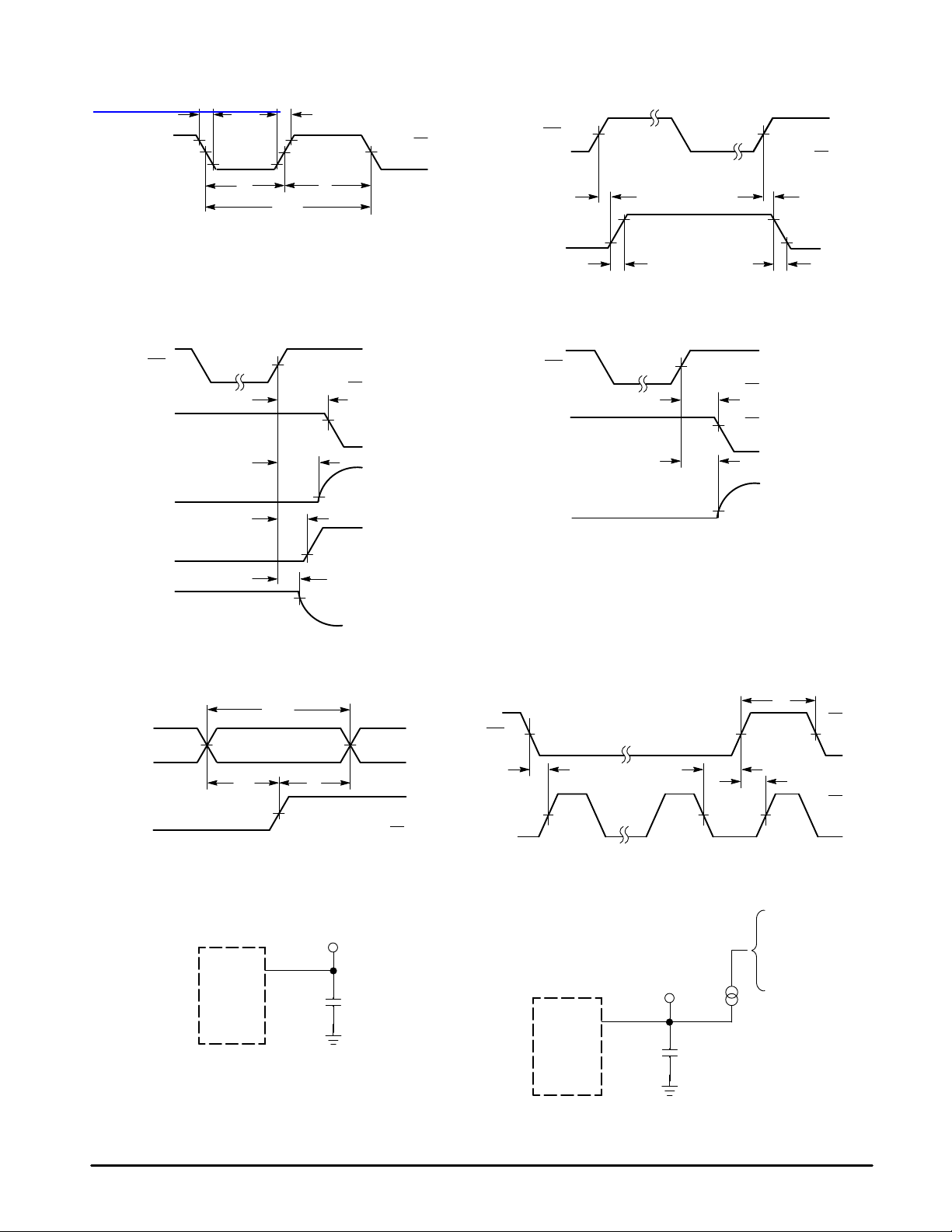
3H. DYNAMIC CHARACTERISTICS OF LOOP AND f
V
= 1.8 to 3.6 V, TA = –40 to 85°C
pos
查询"MC145181"供应商
Symbol
v
Input Voltage Range, f
in
vini
f
Osce
f
Xtal
C
f
*Refer to the Crystal Oscillator Considerations section.
nc...
I
Input Voltage Range, fini
Input Frequency Range, Osc
Crystal Frequency, Oscb and Osc
Input Capacitance of Pins Oscb and
in
Osc
e
Output Frequency Range, f
out
f
Operating Frequency Range of the
φ
Phase/Frequency Detectors, PD
PD
out
Parameter Condition
in
e
out
–Lo, PD
i
out
Figure 9. Figure 10.
e
and f
out
MC145181
PINS
out
Figure
No.
100 MHz ≤ fin < 550 MHz 9 100 300 mVpp
10 MHz ≤ fin < 60 MHz 10 100 400 mVpp
vin = 350 to 600 mVpp,
Device in External Reference Mode
Device in Crystal Mode * 9 80 MHz
Output Signal Swing > 300 mVpp per
out
pin (600 mVpp differential)
–Hi,
11 9 80 MHz
12 1 6.2 MHz
Min Max Unit
— — pF
dc 600 kHz
cale Semiconductor,
Frees
Sine Wave
Generator
Z
= 50
out
Sine Wave
Generator
100 pF
Ω
V
RF
Meter
RL = 50
50
Ω
in
Ω
Figure 11.
0.1
V
in
No
Connection
µ
F
Osc
Osc
Gnd
f
in
f
in
100 pF
e
Device
Under
Test
b
Device
Under
Gnd
V
pos
Test
V
pos
V
pos
V
pos
Sine Wave
Generator
Z
= 50
out
Ω
RF
Meter
Ω
RL = 50
f
out
Device
Under
Test
f
out
100 pF
V
in
Figure 12.
20 pF
20 pF
f
i
in
Device
Under
Test
Gnd
V
Peak–to–peak
Voltage
Measurement
V
V
pos
V
pos
8
For More Information On This Product,
Go to: www.freescale.com
MOTOROLA RF/IF DEVICE DATA
Page 9

nc...
I
cale Semiconductor,
Frees
Freescale Semiconductor, Inc.
MC145181
4. DEVICE OVERVIEW
Refer to the Block Diagram in Section 1.
查询"MC145181"供应商
4A. SERIAL INTERFACE AND REGISTERS
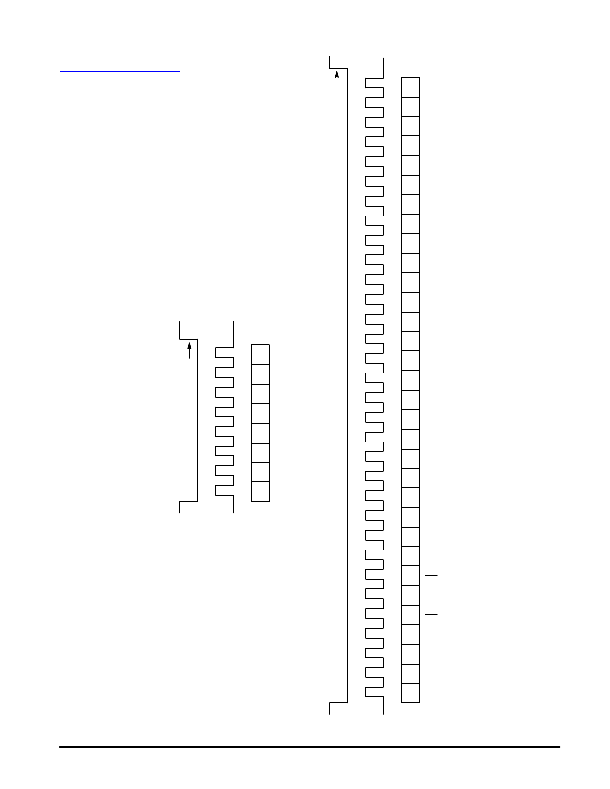
The serial interface is comprised of a Clock pin (Clk), a
Data In pin (Din), and an Enable pin (Enb
data input pin is shifted into a shift register on the low–to–high
transition of the serial clock. The data format is most
significant bit (MSB) first. Both Clk and Enb
Schmitt–triggered inputs.
The R and N registers contain counter divide ratios for the
main loop, PLL. The Ri and Ni registers contain counter
divide ratios for the secondary loop, PLLi. Additional contol
bits are located in the Ri, N, and C registers. The D register
controls the digital–to–analog converters (DACs). Random
access is allowed to the N, Ri, Hr, Hni, D, and C registers.
Two 16–bit holding registers, Hr and Hni, feed registers R
and Ni, respectively. [The three least significant bits (LSBs)
of the Hni register are not used.] The R and Ni registers
determine the divide ratios of the R and Ni counters,
respectively. Thus, the information presented to the R and N
counters is double–buffered. Using the proper programming
sequence, new divide ratios may be presented to the N, R,
and Ni counters; simultaneously .
Enb
is used to activate the data port and allow transfer of
data. To ensure that data is accepted by the device, the Enb
signal line must initially be a high voltage (not asserted), then
make a transition to a low voltage (asserted) prior to the
occurrence of a serial clock, and must remain asserted until
after the last serial clock of the burst. Serial data may be
transferred in an SPI format (while Enb
Data is transferred to the appropriate register on the rising
edge of Enb
BitGrabber in the table, allows access to certain registers
without requiring address bits. When Enb
Clk is inhibited from shifting the shift register.
The serial input pins may NOT be driven above the supply
voltage applied to the V
4B. REFERENCE INPUT AND COUNTERS CIRCUITS
Reference (Oscillator) Circuit
For the Colpitts reference oscillator, one pin ties to the
base (Oscb, pin 32) and the other ties to the emitter (Osce,
pin 1), of an on–chip NPN transistor. In addition, the
reference circuit may be operated in the external reference
(XRef) mode as selectable via bit C6 when the Mode pin is
high.
The Oscb and Osce pins support an external fundamental
or overtone crystal. The output of the oscillator is routed to
both the reference counter for the main loop (R counter) and
the reference counter for the secondary loop (Ri counter).
In a second mode, determined by bit C6 being 1 and the
Mode pin being high, Osce is an input which accepts an
ac–coupled signal from a TCXO or other source. Oscb must
be floated. If the Mode pin is low, this “XRef mode” is not
allowed.
(see Table 1). “Short shifting”, depicted as
pins.
pos
). Information on the
are
remains asserted).
is inactive (high),
Reference Counter for Main Loop
Main reference counter R divides down the frequency at
Osce and feeds the phase/frequency detector for the main
loop. The detector feeds the two charge pumps with outputs
PD
–Hi and PD
out
determined by bits in the R register.
Reference Counter for Secondary Loop
Secondary reference counter Ri divides down the
frequency at Osce and feeds the phase/frequency detector
for the secondary loop. The detector output is PD
division ratio of the Ri counter is determined by the 16 LSBs
of the Ri register.
The Ri counter has a special mode to provide a frequency
output at pins f
low–jitter ECL–type outputs. With the Mode pin low, software
control allows the Osce frequency to be divided–by–8, –10,
or –12.5 and routed to the f
tapping off of a front–end stage of the Ri counter and feeding
the auxiliary counter which provides the divided–down
frequency. The chip must have the Mode pin low, which
activates the f
i
divisible by 2 or 2.5 when the f
no such restriction when the Mode pin is high. See
Section 6D, Ri Register.
4C. LOOP DIVIDER INPUTS AND COUNTER CIRCUITS
fin Inputs and Counter Circuit
fin and f
feeds the N counter. A small signal can feed these inputs
either differentially or single–ended.
The N counter divides down the external VCO frequency
for the main loop. (The divide ratio of the N counter is also
known as the loop multiplying factor.) The divide ratio of this
counter is determined by the 18 LSBs of the N register. The
output of the N counter feeds the phase/frequency detector
for the main loop.
fini
Input and Counter Circuit
fini
the Ni counter. A small signal can feed this input
single–ended.
The Ni counter divides down the external VCO frequency
for the secondary loop. (The divide ratio of the Ni counter is
also known as the loop multiplying factor.) The divide ratio of
this counter is determined by bits in the Ni register. The
output of the Ni counter feeds the phase/frequency detector
for the secondary loop.
4D. VOLTAGE MULTIPLIER AND KEEP–ALIVE
The voltage multiplier produces approximately two times
the voltage present at the V
1.8 V to about 2.5 V. With a supply range of approximately
2.5 V to 3.6 V, the elevated voltage is regulated/limited to
approximately 5 V . The elevated voltage, present at the C
are high–frequency inputs to the amplifier which
in
is the high–frequency input to the amplifier which feeds
CIRCUITS
–Lo. The division ratio of the R counter is
out
and f
out
pins. The actual Ri divide ratio must be
out
(differential outputs). These are
out
pins. This output is derived by
out
pins are activated. There is
out
pins over a supply range of
pos
out
i
. The
mult
MOTOROLA RF/IF DEVICE DATA
For More Information On This Product,
Go to: www.freescale.com
9
Page 10

Freescale Semiconductor, Inc.
pin, is applied to both phase detectors. An external capacitor
to Gnd is required on the C
查询"MC145181"供应商
required for the multiplier are on–chip.
A capacitor to Gnd is also required on the C
voltage on this pin is equal to the voltage on the V
over a supply range of 1.8 V to about 2.5 V. The voltage on
C
is limited to approximately 2.5 V maximum when the
reg
V
pins exceed 2.5 V.
pos
The refresh rate determines the repetition rate that the
capacitors for the voltage multiplier are charged. Refresh is
normally derived off of the signal present at the Osce pin,
through a divider which is part of the voltage multiplier and
regulator circuitry . The refresh rate is controlled via bits in the
Ri register.
When the reference oscillator circuit is placed in standby,
an on–chip keep–alive oscillator assists in maintaining the
elevated voltage on the phase detectors. The keep–alive
refresh rate is per the spec table in Section 3F.
If desired, the keep–alive oscillator can be inhibited from
turning on, by placing the multiplier in the inactive state via R
register bits. This causes the phase/frequency detector
nc...
I
voltage to bleed off while in standby , but has the advantage of
achieving the lowest supply current if all other sections of the
chip are shut down.
pin. The other capacitors
mult
pin. The
reg
MC145181
pins
pos
i
Detector for Secondary Loop
The detector for the secondary loop senses the phase and
frequency difference between the outputs of the Ri and N
counters. Detector output PD
with a three–state push–pull driver.
The output can be forced to the floating state by a bit in the
C register. This facilitates introduction of modulation into the
VCO input.
4F. LOCK DETECTORS
Window counters in each of the lock detector circuits
determine the lock detector phase threshold for PLL and
PLLi. The window counter divide ratio for the main loop’s lock
detector is controlled via a bit in the N register. The window
counter divide ratio for the secondary loop is not controllable
by the user.
The lock detector window determines a minimum phase
difference which must occur before the Lock Detect pin goes
high. Note that the lock detect signals for each loop drive an
AND gate, which then feeds the LD pin. The LD pin indicates
the condition of both loops, or the one active loop if the other
is in standby . If both loops are in standby , LD is low indicating
unlocked.
i
is a voltage–type output
out
i
cale Semiconductor,
Frees
4E. PHASE/FREQUENCY DETECTORS
Detector for Main Loop
The detector for the main loop senses the phase and
frequency difference between the outputs of the R and N
counters. The detector feeds both a high–current charge
pump with output PD
with output PD
The charge pumps can be operated in three conventional
manners as controlled by bits in the N register. PD
be enabled with PD
can be enabled with PD
enabled and tied together externally for maximum charge
pump current. Finally, both outputs can be inhibited. In this
last case, they float. The outputs can also be forced to the
floating state by a bit in the C register. This facilitates
introduction of modulation into the VCO input.
The charge pumps can be operated in an adapt mode as
controlled by bits in the N register. The bits essentially
program a timer which determines how long PD
active. After the time–out, PD
becomes active. In addition, a second set of R and N counter
values can be engaged after the time–out. For more
information, see Table 16 and Section 8, Programmer’s
Guide.
out
–Hi and a low–current charge pump
out
–Lo.
–Hi inhibited. Conversely, PD
out
–Lo inhibited. Both outputs can be
out
–Hi floats and PD
out
out
out
–Lo can
–Hi
out
–Hi is
–Lo
out
4G. DACs
The two independent 8–bit DACs facilitate crystal
oscillator trimming and PA output power control. They are
also suitable for any general–purpose use.
Each DAC utilizes an R–2R ladder architecture. The
output pins, DAC1 and DAC2, are directly connected to the
ladder; that is, there is no on–chip buffer.
The DAC outputs are determined by the contents of the D
register. When a DAC output is zero scale, it is also in a
low–power mode. The power–on reset (POR) circuit
initializes the DACs in the low–power mode upon power up.
4H. GENERAL–PURPOSE OUTPUTS
There are three outputs which may be used as port
expanders for a microcontroller unit (MCU).
Output A is actually a multi–purpose output with a
push–pull output driver. See Table 2 for details.
Output B is a three–state output. The state of Output B
depends on two bits; one of these bits also controls whether
the main PLL is in standby or not. See Table 5 for details.
Output C is an open–drain output. The state of this output
is controlled by one bit per Table 4. Output C is specified with
a guaranteed ON resistance, and thus, may be used in an
analog fashion.
10
For More Information On This Product,
Go to: www.freescale.com
MOTOROLA RF/IF DEVICE DATA
Page 11
Á
Á
Á
Á
Á
Á
Á
Á
Á
Á
Á
Á
nc...
I
cale Semiconductor,
Frees
Freescale Semiconductor, Inc.
MC145181
5. PIN DESCRIPTIONS
5A. DIGITAL PINS
查询"MC145181"供应商
Enb
, Din, and Clk
Pins 5, 6, and 7 — Serial Data Port Inputs
The Enb
allow the transfer of data to the device. T o transfer data to the
device, the Enb
data is being clocked in. When Enb
(inactive), data is transferred to the appropriate register
depending either on the data stream length or address bits.
The C, Hr, and N registers can be accessed using either a
unique data stream length (BitGrabber) or by using address
bits (Conventional). The D, Hni, and Ri registers can only be
accessed using address bits. See Table 1.
The bit stream begins with the MSB and is shifted in on the
low–to–high transition of Clk. The bit pattern is 1 byte (8 bits)
long to access the C register, 2 bytes (16 bits) to access the
Hr register, or 3 bytes (24 bits) to access the N register. A bit
pattern of 4 bytes (32 bits) is used to access the registers
when using address bits. The device has double buffers for
storage of the Ni and R counter divide ratios. One double
buffer is composed of the Hr register which feeds the R
register. An Hr to R register transfer occurs whenever the N
register is written. The other double buffer is the Hni register
which feeds the Ni register. An Hni to Ni register transfer
occurs whenever the N register is written. Thus, new divide
ratios may be presented to the R, Ni, and N counters
simultaneously.
Transitions on Enb
high. This puts the device out of synchronization with the
microcontroller. Resynchronization occurs whenever Enb
high (inactive) and Clk is low.
input is used to activate the serial interface to
pin must be low during the interval that the
is taken back high
must not be attempted while Clk is
is
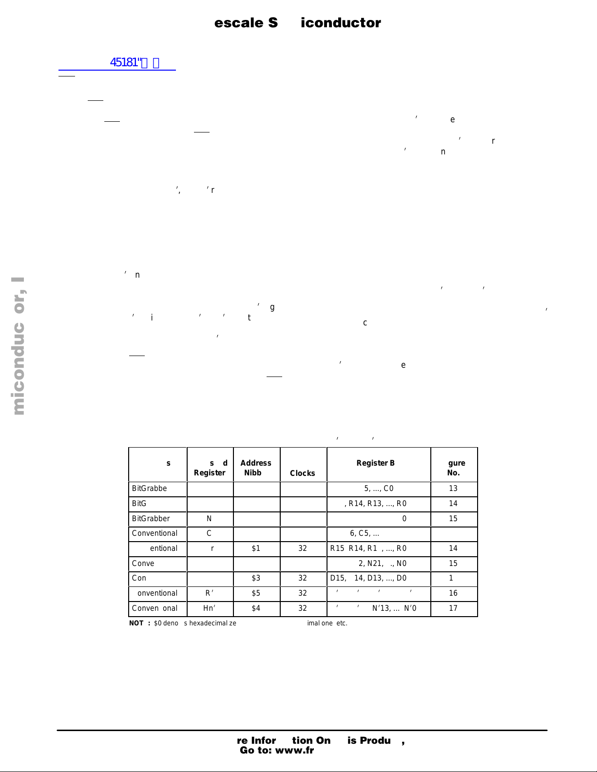
T able 1. Register Access
(LSBs are C0, R0, N0, D0, Ri0, and Ni0)
ÁÁÁ
Access
Type
ÁÁÁ
BitGrabber
BitGrabber
BitGrabber
Conventional
Conventional
Conventional
Conventional
Conventional
Conventional
NOTE: $0 denotes hexadecimal zero, $1 denotes hexadecimal one, etc.
ÁÁ
Accessed
Register
ÁÁ
C
Hr
N
C
Hr
N
D
R
i
Hn
i
ÁÁ
Address
Nibble
ÁÁ
—
—
—
$0
$1
$2
$3
$5
$4
Number
ÁÁ
of
Clocks
ÁÁ
8
16
24
32
32
32
32
32
32
Data is retained in the registers over a supply range of 1.8
to 3.6 V. The bit–stream formats are shown in Figures 13
through 18.
LD
Pin 8 — Lock Detectors Output
This signal is the logical AND of the lock detect signals
from both PLL and PLLi. For the main PLL, the phase
window that defines “lock” is programmable via bit N22. The
phase window for the secondary PLLi is not programmable.
If either PLL or PLLi is in standby, LD indicates the lock
condition of the active loop only. If both loops are in standby,
the LD output is a static low level.
Each PLL’s lock detector is in the high state when the
respective loop is locked (the inputs to the phase detector
being the same phase and frequency). The lock detect signal
is in the low state when a loop is out of lock. See Figure 19.
Upon power up, the LD pin indicates a
not locked
condition. The LD pin is a push–pull CMOS output. If unused,
LD should be left open.
Output A
Pin 9 — Multiple–Purpose Digital Output
Depending on control bits Ri21 and Ri20, Output A is
selectable by the user as a general–purpose output (either
high or low level), fR (output of main reference counter), fRi
(output of secondary reference counter), or a phase detector
pulse indicator for both loops. When selected as
general–purpose output, bit C7 determines whether the
output is a high or low level per Table 2. When configured as
fR, fRi
, or phase detector pulse, Output A appears as a
normally low signal and pulses high.
Output A is a slew–rate limited CMOS totem–pole output.
If unused, Output A should be left open.
ББББББ
Register Bit
Nomenclature
ББББББ
C7, C6, C5, ..., C0
R15, R14, R13, ..., R0
N23, N22, N21, ..., N0
C7, C6, C5, ..., C0
R15, R14, R13, ..., R0
N23, N22, N21, ..., N0
D15, D14, D13, ..., D0
Ri23, Ri22, Ri21, ..., Ri0
Ni15, Ni14, Ni13, ..., Ni0
ÁÁ
Figure
No.
ÁÁ
13
14
15
13
14
15
18
16
17
MOTOROLA RF/IF DEVICE DATA
For More Information On This Product,
Go to: www.freescale.com
11
Page 12
Á
Á
Á
Á
Á
Á
Á
Á
Á
Á
Á
Á
Á
Á
Á
Á
Á
Á
Á
Á
Á
Á
Á
Á
Á
Á
Á
Á
Á
Á
Á
Á
Á
Á
Á
Á
Á
Á
nc...
I
cale Semiconductor,
Frees
Freescale Semiconductor, Inc.
MC145181
Table 2. Output A Configuration
Bit
查询"MC145181"供应商
Ri21
ÁÁ
0
ÁÁ
0
ÁÁ
0
1
1
ÁÁ
Bit
Ri20
ÁÁ
0
ÁÁ
0
ÁÁ
1
0
1
ÁÁ
Bit
C7
Á
0
Á
1
Á
x
x
x
Á
Function of Output A
ББББББ
General–Purpose Output,
ББББББ
Low Level
General–Purpose Output,
ББББББ
High Level
f
R
fRi
Phase Detector Pulse
Indicator
ББББББ
Mode
Pin 10 — Mode Input
When the Mode pin is tied low (approximately Gnd), the
pair of pins named f
and f
. As such, these pins are the divided down reference
out
/Poli and f
out
/Pol become outputs f
out
out
frequency . The division ratio is controlled by bits per Table 6.
In addition, when Mode is low, the Ri counter is preceded by
a fixed–divide prescaler. Also, only a crystal may be used at
pins Oscb and Osce; an external reference, such as a TCXO,
should not be used to drive either pin. The default on the
phase detector polarity is positive. See the summary in
Table 3.
When the Mode pin is tied high (approximately V
pair of pins named f
/Poli and f
out
/Pol become inputs Pol
out
pos
), the
and Pol. As such, these pins control the polarity of the
phase/frequency detectors for PLLi and PLL, respectively . In
addition, when Mode is high, the Ri counter is preceded by a
dual–modulus prescaler. Therefore, the Ri counter is
completely programmable per Figure 16. Also, either a
crystal or TCXO may be used with the device. See the
summary in Table 3.
T able 3. Mode Pin Summary
Attribute
f
/Poli pin
out
ÁÁÁ
f
/Pol pin
out
ÁÁÁ
ÁÁÁ
Oscillator
circuit
Ri counter
ÁÁÁ
Output B
pin
ÁÁÁ
ÁÁÁ
Mode Pin = Low Level
Pin is f
polarity of phase
detectori is positive
Pin is f
polarity of phase
detector is positive
output;
out
БББББ
output;
out
БББББ
БББББ
Supports a crystal only
Programmable in
БББББ
increments of 2 or 2.5
State of pin controlled
by Bit C6
БББББ
БББББ
Mode Pin = High Level
Pin is Poli input and
controls polarity of
БББББ
phase detector
i
Pin is Pol input and
БББББ
controls polarity of
phase detector
БББББ
Supports crystal or
accommodates TCXO
Programmable in
БББББ
increments of 0.5
Pin not used, Bit C6
controls whether
БББББ
crystal or TCXO is
БББББ
accommodated
Output C
Pin 16 — General–Purpose Digital Output
This pin is controllable by bit C5 as either low level or high
impedance per Table 4.
The output driver is an open–drain N–channel MOSFET
connected to Gnd. The ESD (electrostatic discharge)
protection circuit for this pin is tied to Gnd and V
pos
. Thus,
voltages above V
above V
. If unused, Output C should be left open.
pos
are clipped at approximately 0.7 V
pos
Table 4. Output C Programming
Bit C5
0
ÁÁ
1
ÁÁ
State of Output C Pin
Low level
(ON resistance per
БББББББ
Electrical Table)
High impedance
БББББББ
(leakage per Electrical Table)
Output B
Pin 25 — General–Purpose Digital Output
This pin is controllable by bits C6 and C1 as either low
level, high level, or high impedance per Table 5. Note that
whenever the main PLL is placed in standby by bit C1, Output
B is forced to high impedance. The three–state MOSFET
output is slew–rate limited. If unused, Output B should be left
open.
Table 5. Output B Programming
State of
Bit C6
i
*Power–up default.
f
/Poli and f
out
Bit C1
0
0
1
1
0
1
0
1
out
Output B Pin
Low level
High impedance*
High level
High impedance
/Pol
Condition of
Main PLL
Standby*
Standby
Pins 28 and 27 — Dual–purpose Outputs/Inputs
These pins are outputs when the Mode pin is low and
inputs when the Mode pin is high.
When the Mode pin is low, these pins are small–signal
differential outputs f
out
and f
with a frequency derived from
out
the signal present at the Osce pin. The frequency of the
output signal is per Table 6. If this function is not needed, the
Mode pin should be tied high, which minimizes supply
current. In this case, these inputs must be tied high or low per
Tables 7 and 8.
T able 6. f
out
and f
Frequency
out
(Mode Pin = Low)
Bit N23
0
0
0
0
1
1
1
1
Bit Ri1
0
0
1
1
0
0
1
1
Bit Ri0
0
1
0
1
0
1
0
1
Output Frequency
Osce divided by 10
Osce divided by 12.5
Osce divided by 12.5
Osce divided by 12.5
Osce divided by 8
Osce divided by 10
Osce divided by 10
Osce divided by 10
Active
Active
12
For More Information On This Product,
Go to: www.freescale.com
MOTOROLA RF/IF DEVICE DATA
Page 13
Á
Á
Á
Á
Á
Á
Á
Á
Á
Á
Á
Á
Á
Á
Á
Á
Á
Freescale Semiconductor, Inc.
MC145181
When the Mode pin is high, these pins are digital inputs
Poli and Pol which control the polarity of the phase/frequency
查询"MC145181"供应商
detectors. See Tables 7 and 8. Positive polarity is used when
an increase in an external VCO control voltage input causes
an increase in VCO output frequency. Negative polarity is
used when a decrease in an external VCO control voltage
input causes an increase in VCO output frequency.
T able 7. Main Phase/Frequency Detector Polarity
(Mode Pin = High)
ÁÁ
Mode Pin
High
High
Low
*Pin configured as an output; should not be driven.
ÁÁ
Pol Pin
Low
High
*
Main Detector Polarity
БББББББ
(PD
–Lo and PD
out
Positive
Negative
Positive
out
–Hi)
5C. LOOP PINS
fin and f
in
Pins 12 and 13 — Frequency Input for Main Loop (PLL)
These pins feed the on–chip RF amplifier which drives the
high–speed N counter. This input may be fed differentially.
However, it is usually used in a single–ended configuration
with fin driven while f
is tied to a good RF ground (via a
in
capacitor). The signal source driving this input must be ac
coupled and originates from an external VCO.
The sensitivity of the RF amplifier is dependent on
frequency as shown in the Loop Specifications table.
Sensitivity of the fin input is specified as a level across a 50 Ω
load driven by a 50 Ω source. A VCO that can drive a load
within the data sheet limits can also drive fin. Usually , to avoid
load pull and resultant frequency modulation of the VCO, fin is
lightly coupled by a small value capacitor and/or a resistor.
See the applications circuit of Figure 65.
nc...
I
cale Semiconductor,
Frees
T able 8. Secondary Phase/Frequency
Detector Polarity
(Mode Pin = High)
ÁÁ
Mode Pin
ÁÁ
High
High
Low
*Pin configured as an output; should not be driven.
ÁÁ
Poli Pin
ÁÁ
Low
High
*
Secondary Detector
БББББ
Polarity
(PD
i
БББББ
out
Positive
Negative
Positive
)
5B. REFERENCE PINS
Osce and Osc
b
Pins 1 and 32 — Reference Oscillator Transistor Emitter
and Base
These pins can be configured to support an external
crystal in a Colpitts oscillator configuration. The required
connections for the crystal circuit are shown in the Crystal
Oscillator Considerations section.
Additionally, the pins can be configured to accept an
external reference frequency source, such as a TCXO. In this
case, the reference signal is ac coupled into Osce and the
Oscb pin is left floating. See Figure 1 1.
Bit C6 and the Mode input pin control the configuration of
these pins per Table 9.
fini
Pin 30 — Frequency Input for Secondary Loop (PLLi)
This pin feeds the on–chip RF amplifier which drives the
high–speed Ni counter. This input is used in a single–ended
configuration. The signal source driving this input must be ac
coupled and originates from an external VCO.
The sensitivity of the RF amplifier is dependent on
frequency as shown in the Loop Specifications table.
Sensitivity of the fini
input is specified as a level across a
50 Ω load driven by a 50 Ω source. A VCO that can drive a
load within the data sheet limits can also drive fini
. Usually , to
avoid load pull and resultant frequency modulation of the
VCO, fini
is lightly coupled by a small value capacitor and/or
a resistor. See the applications circuit of Figure 65.
If the secondary loop is not used, PLLi should be placed in
standby and fini
PD
–Hi and PD
out
should be left open.
–Lo
out
Pins 19 and 20 — Phase/Frequency Detector Outputs
for Main Loop (PLL)
Each pin is a three–state current source/sink/float output
for use as a loop error signal when combined with an external
low–pass loop filter. Under bit control, PD
one–quarter or one–eighth the output current of PD
–Lo has either
out
out
–Hi per
Table 10. The detector is characterized by a linear transfer
function (no dead zone). The polarity of the detector is
controllable. The operation of the detector is described below
and shown in Figure 20.
T able 9. Reference Configuration
Mode
ÁÁ
Input
Pin
ÁÁ
Low
High
High
ÁÁ
*See Table 5.
ÁÁ
Bit C6
ÁÁ
ÁÁ1БББББ
БББББ
БББББ
X
Supports Crystal
(default)
0
Supports Crystal
Requires External
Reference
MOTOROLA RF/IF DEVICE DATA
Reference
Configuration
Table 10. Current Ratio of PD
БББББ
Comment
БББББ
C6 used to control
Output B*
Output B not useful
Output B not useful
БББББ
When the Mode pin is high, positive polarity occurs when
Bit
Á
N18
0
1
the Pol pin is low. Also, when the Mode pin is low, polarity
For More Information On This Product,
Go to: www.freescale.com
and PD
Output Current Ratio
PD
ББББББ
–Lo
out
–Hi:PD
out
(Gain Ratio)
4 : 1
8 : 1
out
–Lo
out
–Hi
13
Page 14
Á
Á
Á
Á
Á
Á
Á
Á
Á
Á
Á
Á
Á
Á
Á
Á
Á
Á
Á
Á
Á
nc...
I
cale Semiconductor,
Frees
Freescale Semiconductor, Inc.
MC145181
defaults to positive. Positive polarity is described below. fV is
the output of the main loop’s VCO divider (N counter). fR is
查询"MC145181"供应商
the output of the main loop’s reference divider (R counter).
(a) Frequency of fV > fR or phase of fV leading fR:
current–sinking pulses from a floating state.
(b) Frequency of fV < fR or phase of fV lagging fR:
current–sourcing pulses from a floating state.
(c) Frequency and phase of fV = fR: essentially a floating
state, voltage at pin determined by loop filter.
When the Mode pin is high, negative polarity occurs when
the Pol pin is high. Negative polarity is described below. fV is
the output of the main loop’s VCO divider (N counter). fR is
the output of the main loop’s reference divider (R counter).
(a) Frequency of fV > fR or phase of fV leading fR:
current–sourcing pulses from a floating state.
(b) Frequency of fV < fR or phase of fV lagging fR:
current–sinking pulses from a floating state.
(c) Frequency and phase of fV = fR: essentially a floating
state, voltage at pin determined by loop filter.
These outputs can be enabled and disabled by bits in the
C and N registers. Placing the main PLL in standby (bit C1
= 1) forces the detector outputs to a floating state. In addition,
setting the PD Float bit (bit C4 = 1) forces the detector
outputs to a floating state while allowing the counters to run
for the main PLL. For selection of the outputs, see Table 11.
The phase detector gain (in amps per radian) = PD
out
current (in amps) divided by 2π.
If a detector output is not used, that pin should be left
open.
T able 11. Selection of Main Detector Outputs
Bit
N21
ÁÁ
0
0
0
0
1
ÁÁ
1
ÁÁ
ÁÁ1Á1Á0ББББББББ
1
ÁÁ
ÁÁ
NOTES:1. When a detector output is not enabled, it is floating.
БББББББББББББББ
Bit
N20
Á
0
0
1
1
0
Á
0
Á
1
Á
Á
2. Setting bit N21 = 1 places the IC in an adapt mode and engages a
timer.
Bit
N19
Á
Á
Á
Á
Á
ББББББББ
0
Both outputs not enabled
1
PD
out
0
PD
out
1
Both PD
enabled
0
PD
out
ББББББББ
only, then PD
1
PD
out
only, then PD
ББББББББ
PD
out
only, then PD
1
PD
out
ББББББББ
cycles only, then PD
enabled
ББББББББ
Result
–Lo enabled
–Hi enabled
–Lo and PD
out
–Hi enabled for 16 fR cycles
–Hi enabled for 32 fR cycles
–Hi enabled for 64 fR cycles
–Hi enabled for 128 f
–Lo enabled
out
–Lo enabled
out
–Lo enabled
out
out
out
–Lo
–Hi
R
PD
i
out
Pin 23 — Phase/Frequency Detector Output for
Secondary Loop (PLLi)
This pin is a three–state voltage output for use as a loop
error signal when combined with an external low–pass loop
filter. The detector is characterized by a linear transfer
function (no dead zone). The polarity of the detector is
controllable. The operation of the detector is described below
and shown in Figure 21.
When the Mode pin is high, positive polarity occurs when
the Poli pin is low. Also, when the Mode pin is low, polarity
defaults to positive. Positive polarity is described below. fVi
is
the output of the secondary loop’s VCO divider (Ni counter).
fRi
is the output of the secondary loop’s reference divider (R
counter.)
(a) Frequency of fVi
> fRi
or phase of fVi
leading fRi
negative pulses from high impedance.
(b) Frequency of fVi
< fRi
or phase of fVi
lagging fRi
positive pulses from high impedance.
(c) Frequency and phase of fVi
= fRi
: essentially a
high–impedance state, voltage at pin determined by
loop filter.
When the Mode pin is high, negative polarity occurs when
the Poli pin is high. Negative polarity is described below. fVi
is the output of the secondary loop’s VCO divider (N
counter). fRi
is the output of the secondary loop’s reference
counter (Ri counter.)
(a) Frequency of fVi
> fRi
or phase of fVi
leading fRi
positive pulses from high impedance.
(b) Frequency of fVi
< fRi
or phase of fVi
lagging fRi
negative pulses from high impedance.
(c) Frequency and phase of fVi
= fRi
: essentially a
high–impedance state, voltage at pin determined by
loop filter.
This output can be enabled and disabled by bits in the C
register. Placing the secondary PLLi in standby (bit C0 = 1)
forces the detector output to a high–impedance state. In
addition, setting the PDi Float bit (bit C3 = 1) forces the
detector output to a high–impedance state while allowing the
counters to run for PLLi.
The phase detector gain (in volts per radian) = C
mult
voltage (in volts) divided by 4π.
If the secondary loop is not used, PLLi should be placed in
standby and PD
i
should be left open.
out
5D. ANALOG OUTPUTS
DAC1 and DAC2
Pins 3 and 4 — Digital–to–Analog Converter Outputs
These are independent outputs of the two 8–bit D/A
converters. The output voltage is determined by bits in the D
register. Each output is a static level with an output
impedance of approximately 100 kΩ.
The DACs may be used for crystal oscillator trimming, PA
(power amplifier) output power control, or other
general–purpose use.
If a DAC output is not used, the pin should be left open.
i
:
:
i
:
:
14
For More Information On This Product,
Go to: www.freescale.com
MOTOROLA RF/IF DEVICE DATA
Page 15

5E. EXTERNAL COMPONENTS
Freescale Semiconductor, Inc.
MC145181
5F. SUPPLY PINS
Rx
查询"MC145181"供应商
Pin 17 — Current–Setting Resistor
An external resistor to Gnd at this pin sets a reference
current that is used to determine the current at the
phase/frequency detector outputs PD
A value of 2 kΩ is required.
C
mult
Pin 21 — Voltage–Multiplier Capacitor
An external capacitor to Gnd at this pin is used for the
on–chip voltage multiplier circuit. The value of this capacitor
must be greater than 20 times the value of the largest loop
filter capacitor. For example, if the largest loop filter capacitor
on either the main loop or the secondary loop is 0.01 µF , then
a 0.22 µF capacitor could be used on the C
To ensure minimum standby supply current drain, the
voltage potential at the C
below the potential at the V
keep–alive oscillator is shut off, the user should tie a large
nc...
I
value resistor (> 10 MΩ) between the C
resistor should be sized to overcome leakage from C
Gnd due to the printed circuit board and the external
capacitor. The consequence of not using the resistor is
higher supply current drain in standby . If standby is not used,
the resistor is not necessary . Also, if the keep–alive oscillator
is used, the resistor can be omitted.
pin must not be allowed to fall
mult
pos
–Hi and PD
out
pin.
mult
pins. Therefore, if the
pin and V
mult
out
pos
. This
mult
–Lo.
to
DAC V
pos
Pin 2 — Positive Supply Potential for DACs
This pin supplies power to both DACs and determines the
full–scale output of the DACs. The full–scale output is
approximately equal to the voltage at DAC V
applied to this pin may be more, less, or equal to the potential
applied to the V
1.8 to 3.6 V with respect to the Gnd pins.
If both DACs are not used, DAC V
same potential as V
V
pos
Pins 11, 24, 26, and 29 — Principal Positive Supply
Potential
These pins supply power to the main portion of the chip.
All V
voltage range for V
pins.
together and bypassed to a ground plane using a
low–inductance capacitor mounted very close to the device.
Lead lengths and printed circuit board traces between the
capacitor and the IC package should be minimized. (The
very–fast switching speed of the device can cause excessive
current spikes on the power leads if they are improperly
bypassed.)
pins must be at the same voltage potential. The
pos
For optimum performance, all V
pins. The voltage range for DAC V
pos
should be tied to the
.
pos
is 1.8 to 3.6 V with respect to the Gnd
pos
pos
pins should be tied
pos
. The voltage
pos
pos
is
cale Semiconductor,
Frees
C
reg
Pin 22 — Regulator Capacitor
An external capacitor to Gnd at this pin is required for the
on–chip voltage regulator . A value of 1 µF is recommended.
Gnd
Pins 14, 15, 18, and 31 — Ground
Common ground for the device. All Gnd pins must be at
the same potential and should be tied to a ground plane.
MOTOROLA RF/IF DEVICE DATA
For More Information On This Product,
Go to: www.freescale.com
15
Page 16
Freescale Semiconductor, Inc.
6. DETAILED REGISTER DESCRIPTIONS
查询"MC145181"供应商
6A. C REGISTER
nc...
I
MC145181
Note 4
cale Semiconductor,
Frees
Note 4
Figure 13. C Register Access and Formats
Enb
12345678
Clk
C7 C6 C5 C4 C3 C2 C1 C0
in
D
A3 A2 A1 A0 C7 C6 C5 C4 C3 C2 C1 C0
0
000
16
1 2 3 4 5 6 7 8 9 10 11 12 13 14 15 16 17 18 19 20 21 22 23 24 25 26 27 28 29 30 31 32
Figure 13.
Enb
Clk
For More Information On This Product,
Go to: www.freescale.com
XXXX XXXX XXX XX XXXXXXX
1. To access the C register, either 8 or 32 clock cycles can be used.
2. For the 8–bit stream, no address bits are needed.
3. For the 32–bit stream, address bits A3 through A0 are required.
4. At this point, the new byte is transferred to the C register. No other register is affected.
in
D
MOTOROLA RF/IF DEVICE DATA
NOTES:
5. X signifies a don’t care bit.
Page 17
Á
Á
Á
Á
nc...
I
cale Semiconductor,
Frees
Freescale Semiconductor, Inc.
C REGISTER BITS
See Figure 13 for C register access and serial data
查询"MC145181"供应商
formats.
Out A (C7)
When the Output A pin is selected as a General–Purpose
Output (via bits Ri21 = Ri20 = 0), bit C7 determines the state
of the pin. When C7 is 1, Output A is forced to a high level.
When C0 is 0 Output A is forced low.
When Output A is not selected as a General–Purpose
Output, bit C7 has no function; i.e., C7 is a “don’t care” bit.
Out B/XRef (C6)
Bit C6 is a dual–purpose bit.
When the Mode pin is tied low, C6 and C1 (PLL Stby), can
be used to control Output B. See Table 12. (The reference
circuit defaults to crystal configuration.)
When the Mode pin is tied high, additional control of the
reference circuit is allowed. See Table 13.
Table 12. Out B/XRef Bit with Mode Pin = Low
ÁÁ
ÁÁ
Bit C6
*Power up default.
Table 13. Out B/XRef Bit with Mode Pin = High
Out C (C5)
This bit determines the state of the Output C pin. When C5
is 1, Output C is forced to a high–impedance state. When C5
is 0, Output C is forced low.
PD Float (C4)
This bit controls the phase detector for the main loop,
outputs PD
phase detector operates normally. When the bit is 1, the
outputs are forced to the floating state which opens the loop
and allows modulation to be introduced into the external VCO
input. During this time, the counters are still active. This bit is
inhibited from affecting the phase detector during a PD
or PD
out
If the loop is locked prior to C4 being set to 1, the lock
detect signal from the main loop continues to indicate “lock”
immediately after PD Float is set to 1. If the phase of the loop
drifts outside the lock detect window, then the lock detect
signal indicates “not locked”. If the loop is not locked, and PD
Float is set to 1, then the lock detect signal from the main loop
continues to indicate “not locked”.
Bit C1
0
0*
1
1
*Power up default.
0
1*
0
1
Bit C6
0*
1
–Hi and PD
out
–Lo pulse.
Supports Crystal*
Accommodates External Reference
State of
ÁÁÁÁ
Output B Pin
Low level
High impedance*
High level
High impedance
Reference Configuration
–Lo. When this bit is 0, the main
out
Condition of
ÁÁÁ
Main PLL
Active
Standby*
Active
Standby
MC145181
–Hi
out
PDi Float (C3)
This bit controls the phase/frequency detector for the
secondary loop, output PD
secondary phase detector operates normally . When the bit is
1, the output is forced to the floating state which opens the
loop and allows modulation to be introduced into the external
VCO input. During this time, the counters are still active. This
bit is inhibited from affecting the phase detector during a
PD
i
pulse.
out
If the loop is locked prior to C3 being set to 1, the lock
detect signal from the secondary loop continues to indicate
“lock” immediately after PDi Float is set to 1. If the phase of
the loop drifts outside the lock detect window, then the lock
detect signal indicates “not locked”. If the loop is not locked,
and PDi Float is set to 1, then the lock detect signal from the
secondary loop continues to indicate “not locked”.
Osc Stby (C2)
This bit controls the crystal oscillator and external
reference input circuit. When this bit is 0, the circuit is active.
When the bit is 1, the circuit is shut down and is in the
low–power standby mode. When this circuit is shut down, a
keep–alive oscillator for the voltage doubler is activated,
unless the doubler is shut off via bits in the Ri register. In the
crystal oscillator mode, when C2 transitions from a 1 to a 0
state, a kick–start circuit is engaged for a few milliseconds.
The kick–start circuit ensures self–starting for a
properly–designed crystal oscillator
Whenever C2 is 1, both bits C1 and C0 must be
1, also.
To minimize standby supply current, the voltage multiplier
may be shut down (by bits Ri19, Ri18, and Ri17 being all
zeroes). If this is the case and the voltage multiplier feature is
being used, the user must allow sufficient time for the
phase/frequency detector supply voltage to pump up when
the multiplier is brought out of standby . This “pump up” time is
dependent on the C
approximately 100 µA. During the pump up time, either the
PLL standby bits C1 and C2 must be 1 or the phase/
frequency detector float bits C3 and C4 must be 1.
PLL Stby (C1)
When set to 1, this bit places the main PLL in the standby
mode for reduced power consumption. PD
PD
–Lo are forced to the floating state, the N and R
out
counters are inhibited from counting, the main loop’s input
amp is shut off, the Rx current is inhibited, and the main
phase/frequency detector is shut off. The reference oscillator
circuit is still active and independently controlled by bit C2.
When this bit is programmed to 0, the main PLL is taken
out of standby in two steps. First, the input amplifier is
activated, all counters are enabled, and the Rx current is no
longer inhibited. Any fR and fV signals are inhibited from
toggling the phase/frequency detectors and lock detector at
this time. Second, when the fR pulse occurs, the N counter is
loaded, and the phase/frequency and lock detectors are
initialized via both flip–flops being reset. Immediately after
the load, the N and R counters begin counting down together.
At this point, the fR and fV pulses are enabled to the phase
mult
i
. When this bit is 0, the
out
NOTE
capacitor size. Pump current is
–Hi and
out
MOTOROLA RF/IF DEVICE DATA
For More Information On This Product,
Go to: www.freescale.com
17
Page 18

Freescale Semiconductor, Inc.
and lock detectors, and the phase/frequency detector output
is enabled to issue an error correction pulse on the next f
查询"MC145181"供应商
and fV pulses. (Patent issued on this method.)
During standby, data is retained in all registers and any
register may be accessed. When setting or clearing the PLL
Stby bit, other bits in the C register may be changed
simultaneously.
PLLi Stby (C0)
When set to 1, this bit places the PLLi section of the chip,
which includes the on–chip fini
mode for reduced power consumption. PD
floating state. The Ri and Ni counters are inhibited from
counting and placed in the low–current mode. The exception
is the Ri counter’s prescaler when the Mode pin is low. The
Ri counter’s prescaler remains active along with the f
f
pins when PLLi is placed in standby (Mode pin = low).
out
When the Mode pin is low, the f
nc...
I
input amp, in the standby
pin, f
out
i
is forced to the
out
pin, and R
out
MC145181
R
and
out
i
counter’s prescaler are shut down only when Osc Stby bit C2
is set to 1.
When C0 is reset to 0, PLLi is taken out of standby in two
steps. All PLLi counters and the input amp are enabled. Any
fRi
and fVi
phase/frequency detector at this time. Second, when the fRi
pulse occurs, the Ni counter is loaded and the phase/
frequency detector is initialized via both flip–flops being
reset. Immediately after the load, the Ni and Ri counters
begin counting down together. At this point, the fRi
pulses are enabled to the phase and lock detectors, and the
phase/frequency detector output is enabled to issue an error
correction pulse on the next fRi
on this method.)
During standby, data is retained in all registers, and any
register may be accessed. When setting or clearing the PLL
Stby bit, other bits in the C register may be changed
simultaneously.
signals are inhibited from toggling the associated
and fVi
and fVi
pulses. (Patent issued
i
cale Semiconductor,
Frees
18
For More Information On This Product,
Go to: www.freescale.com
MOTOROLA RF/IF DEVICE DATA
Page 19
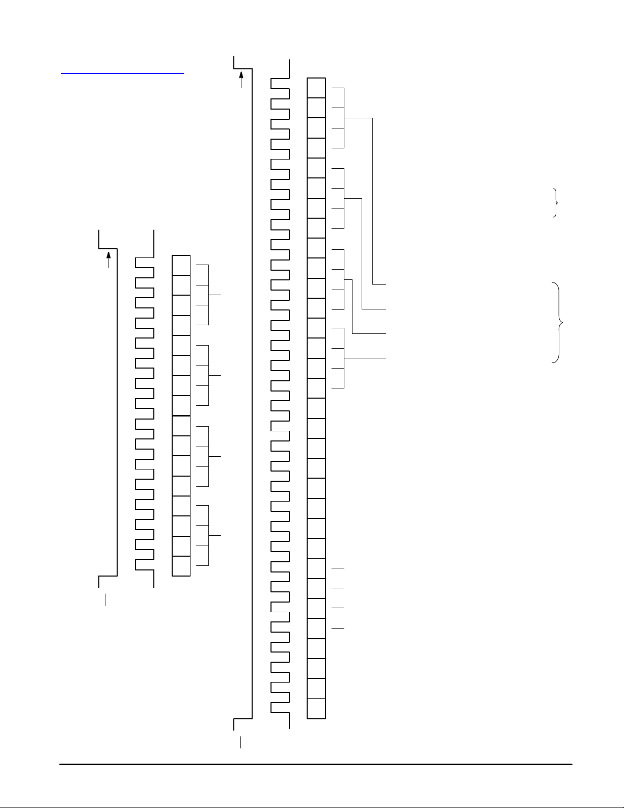
6B. Hr REGISTER
查询"MC145181"供应商
Freescale Semiconductor, Inc.
MC145181
Note 4
Decimal (Note 7)
nc...
I
cale Semiconductor,
Frees
Note 4
910 111213141516
Figure 14. Hr Register Access and Formats
12345678
R7 R6 R5 R4 R3 R2 R1 R0
R15 R14 R13 R12 R11 R10 R9 R8
See Below See Below See Below See Below
Not Allowed
Not Allowed
0
1
...
0
0
...
0
0
...
0
0
...
Not Allowed
Not Allowed
R Counter Ratio = 20.5
R Counter Ratio = 21
R Counter Ratio = 20
6789A
22222
00000
00000
R Counter Ratio = 21.5
B
2
0
0 2 C R Counter Ratio = 220
0...F
R Counter Ratio = 32,767
R Counter Ratio = 32,767.5
...EF
...FF
...FF
Hexadecimal
F
Enb
MOTOROLA RF/IF DEVICE DATA
Clk
in
D
Figure 14.
001
0
in
Enb
1 2 3 4 5 6 7 8 9 10 11 12 13 14 15 16 17 18 19 20 21 22 23 24 25 26 27 28 29 30 31 32
Clk
A3 A2 A1 A0 R7 R6 R5 R4 R3 R2 R1 R0
X X X X X X X X X X X X R15 R14 R13 R12 R11 R10 R9 R8
D
For More Information On This Product,
Go to: www.freescale.com
R combination), either 16 or 32 clock cycles can be used.
1. To access the Hr register (the holding register or first buffer of the double–buffered Hr and
NOTES:
divide ratio is not altered yet and retains the previous ratio loaded. No other register is affected.
2. For the 16–bit stream, no address bits are needed.
3. For the 32–bit stream, address bits A3 through A0 are required.
4. At this point, the two new bytes are transferred to the Hr register. Therefore, the R counter
5. A transfer from Hr (holding) register to the R register occurs with each N register access.
6. X signifies a don’t care bit.
7. The decimal value multiplied by 2 = the hexadecimal value.
19
Page 20
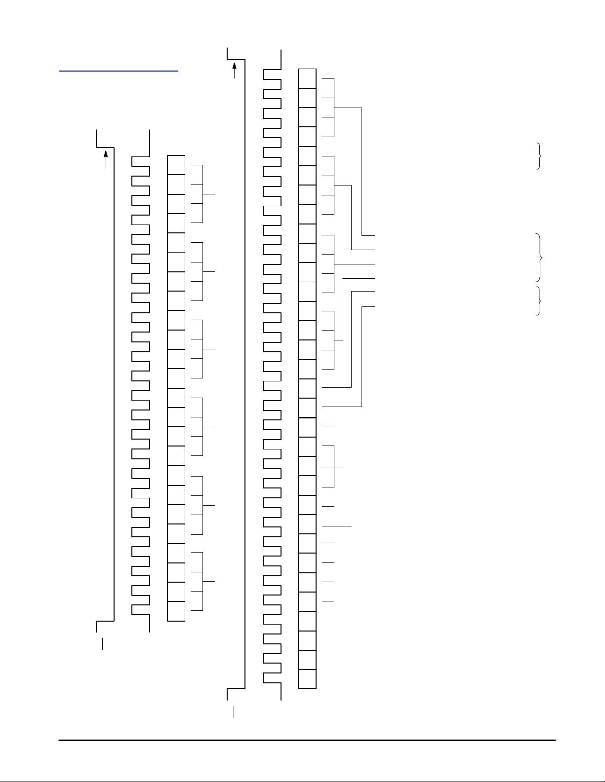
6C. N REGISTER
Freescale Semiconductor, Inc.
MC145181
查询"MC145181"供应商
Note 4
Decimal
Note 4
N Counter Ratio = 992
N Counter Ratio = 993
N Counter Ratio = 994
N Counter Ratio = 995
Not Allowed
Not Allowed
0
1
0
0
0
0
0
nc...
I
17 18 19 20 21 22 23 24
N7 N6 N5 N4 N3 N2 N1 N0N23 N22 N21 N20 N19 N18 N17 N16 N15 N14 N13 N12 N11 N10 N9 N8
See Below See Below
0
0
0
0
0
...
...
...
...
...
...
Not Allowed
Not Allowed
EF012
DDEEE
33333
00000
00000
00000
N Counter Ratio = 996
3
E
E
3
0
03 40
0
0
0
N Counter Ratio = 262,142
N Counter Ratio = 262,143
E
...
...
...
...
...
...
F
F
F
F
F
F
F
1
1
1
1
Hexadecimal
Binary
cale Semiconductor,
Frees
910111213141516
Figure 15. N Register Access and Formats
12345678
Enb
Clk
Ratio
Current
Phase
Detector
Program
LD
Window
Control
010
See Below See Below See Below See Below
in
D
A3 A2 A1 A0 N7 N6 N5 N4 N3 N2 N1 N0
0
20
Figure 15.
Enb
1 2 3 4 5 6 7 8 9 10 11 12 13 14 15 16 17 18 19 20 21 22 23 24 25 26 27 28 29 30 31 32
Clk
X X X X N23 N22 N21 N20 N19 N18 N17 N16 N15 N14 N13 N12 N11 N10 N9 N8
in
D
For More Information On This Product,
Go to: www.freescale.com
R and Hn’ to N’ transfer occurs.
1. To access the N register, either 24 or 32 clock cycles can be used.
2. For the 24–bit stream, no address bits are needed.
3. For the 32–bit stream, address bits A3 through A0 are required.
4. At this point, the three new bytes are transferred to the N register. In addition, an Hr to
NOTES:
MOTOROLA RF/IF DEVICE DATA
5. X signifies a don’t care bit.
Page 21
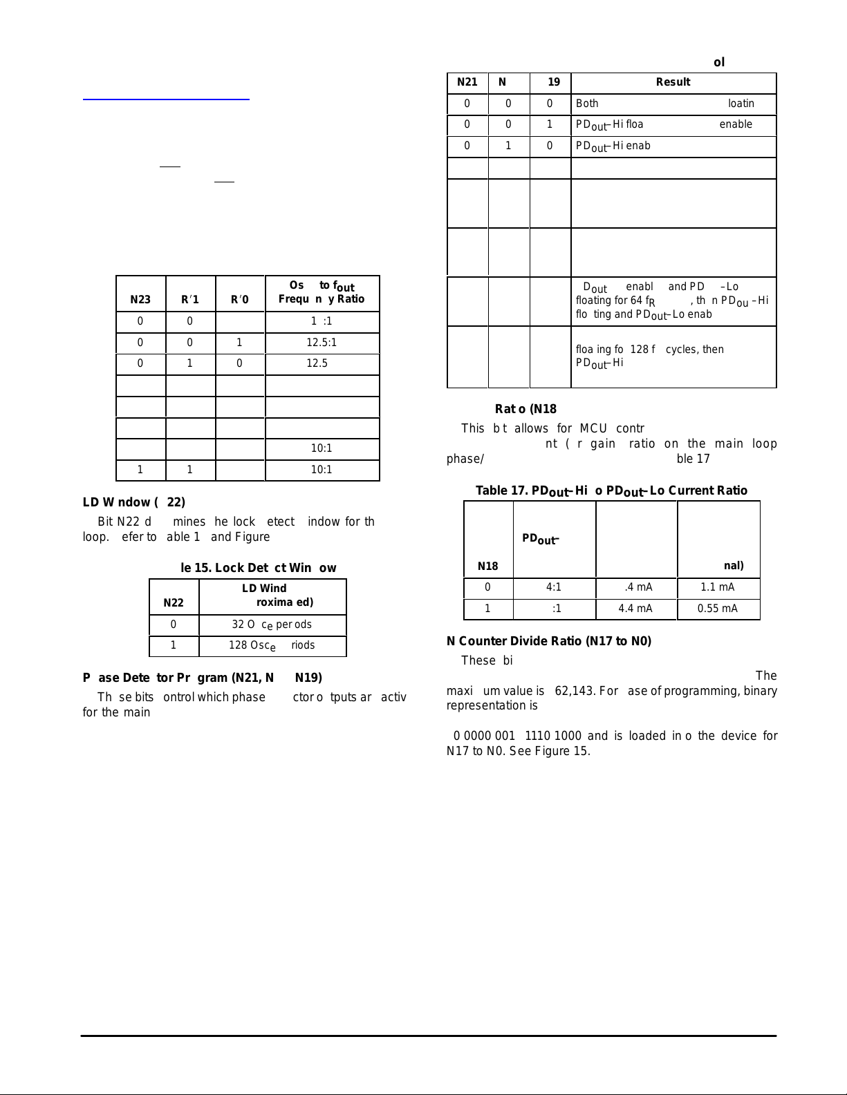
Á
Á
Á
Á
Á
Á
Á
Á
Á
Á
Á
Á
Á
Á
Á
Á
Á
Á
Á
Á
Á
Á
Á
Á
Á
Á
Á
Á
Á
Á
Á
Á
Á
Á
Á
Á
Á
nc...
I
cale Semiconductor,
Frees
Freescale Semiconductor, Inc.
MC145181
N REGISTER BITS
See Figure 15 for N register access and serial data
查询"MC145181"供应商
formats.
Control (N23)
When the Mode pin is low, Control bit N23 determines the
divide ratio of the auxiliary divider which feeds the buffers for
the f
out
and f
between Osce and f
pins. See Table 14 for the overall ratio
out
out
/f
.
out
When the Mode pin is high, N23 must be programmed
to 1.
T able 14. Osce to f
Frequency Ratio,
out
Mode = Low
Á
N23
0
0
0
0
1
1
1
1
ÁÁ
Ri1
0
0
1
1
0
0
1
1
Á
Ri0
0
1
0
1
0
1
0
1
Osce to f
ÁÁÁÁ
Frequency Ratio
out
10:1
12.5:1
12.5:1
12.5:1
8:1
10:1
10:1
10:1
LD Window (N22)
Bit N22 determines the lock detect window for the main
loop. Refer to Table 15 and Figure 19.
T able 15. Lock Detect W indow
LD Window
N22
ÁÁ
ÁÁ0ББББББ
ÁÁ1ББББББ
(Approximated)
ББББББ
32 Osce periods
128 Osce periods
Phase Detector Program (N21, N20, N19)
These bits control which phase detector outputs are active
for the main loop. These bits also control the timer interval
when adapt is utilized for the main loop. See Table 16.
T able 16. Main Phase Detector Control
N21
N20
0
0
0
0
ÁÁ1Á
1
ÁÁ
ÁÁ
ÁÁ
ÁÁ
Á
Á
1
Á
Á
1
ÁÁ
ÁÁ
Á
Á
N19
0
0
1
1
0
0
1
1
Á
Á
Á
Á
Á
Á
Á
0
Both PD
1
PD
–Hi floating, PD
out
0
PD
–Hi enabled, PD
out
1
Both PD
0
PD
–Hi enabled and PD
out
floating for 16 fR cycles, then PD
БББББББББ
floating and PD
1
PD
–Hi enabled and PD
out
БББББББББ
floating for 32 fR cycles, then PD
floating and PD
БББББББББ
0
PD
–Hi enabled and PD
out
БББББББББ
floating for 64 fR cycles, then PD
floating and PD
БББББББББ
1
PD
–Hi enabled and PD
out
floating for 128 fR cycles, then
БББББББББ
PD
–Hi floating and PD
out
enabled
БББББББББ
–Hi and PD
out
–Hi and PD
out
Result
out
–Lo enabled
out
–Lo enabled
out
–Lo enabled
out
–Lo floating
out
–Lo enabled
–Lo floating
out
–Lo enabled
out
–Lo
out
–Lo
out
–Lo
out
–Lo
out
–Lo
out
out
out
out
–Hi
–Hi
–Hi
Current Ratio (N18)
This bit allows for MCU control of the PD
PD
–Lo current (or gain) ratio on the main loop
out
out
–Hi to
phase/frequency detector outputs. See Table 17.
T able 17. PD
ÁÁ
ÁÁ
Current Ratio
N18
ÁÁ
0
1
PD
–Hi to PD
out
ÁÁÁ
–Hi to
out
ÁÁÁ
PD
–Lo
out
ÁÁÁ
4:1
8:1
–Lo Current Ratio
out
PD
–Hi
out
Current
ÁÁÁ
C
mult
ÁÁÁ
Pin = 5 V
(Nominal)
ÁÁÁ
4.4 mA
4.4 mA
PD
–Lo
out
Current
ÁÁÁ
C
mult
ÁÁÁ
Pin = 5 V
(Nominal)
ÁÁÁ
1.1 mA
0.55 mA
N Counter Divide Ratio (N17 to N0)
These bits control the N Counter divide ratio or loop
multiplying factor. The minimum allowed value is 992. The
maximum value is 262,143. For ease of programming, binary
representation is used. For example, if a divide ratio of 1000
is needed, the 1000 in decimal is converted to binary
00 0000 0011 1110 1000 and is loaded into the device for
N17 to N0. See Figure 15.
MOTOROLA RF/IF DEVICE DATA
For More Information On This Product,
Go to: www.freescale.com
21
Page 22
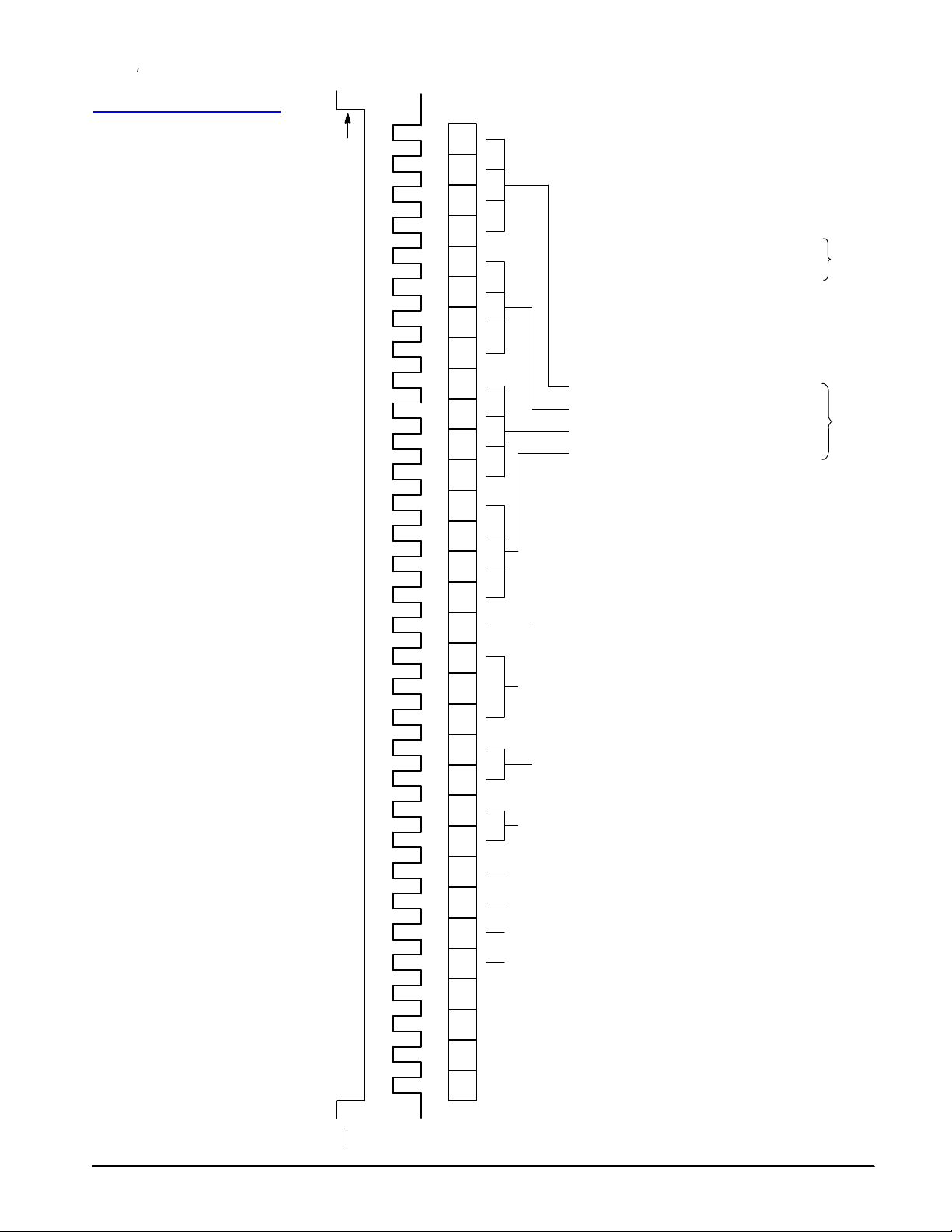
6D. Ri REGISTER
Freescale Semiconductor, Inc.
MC145181
查询"MC145181"供应商
Note 3
Decimal (Note 4)
Not Allowed
Not Allowed
0
1
0
0
0
nc...
I
0
0
0
...
...
...
...
Not Allowed
Not Allowed
R’ Counter Ratio = 20
R’ Counter Ratio = 20.5
6789A
22222
00000
00000
R’ Counter Ratio = 21
R’ Counter Ratio = 21.5
R’ Counter Ratio = 22
B
2
2
0
0
00 C
R’ Counter Ratio = 32,767
E
...
...
F
...
F
...
F
R’ Counter Ratio = 32,767.5
F
F
F
Hexadecimal
F
cale Semiconductor,
Frees
Figure 16. R’ Register Access and Format
A3 A2 A1 A0 R’7 R’6 R’5 R’4 R’3 R’2 R’1 R’0
T st/Rst
(User must
Program to 0)
Control
Function
Output A
Y V–Mult
Coefficient
101
0
22
Figure 16.
X X X X R’23 R’22 R’21 R’20 R’19 R’18 R’17 R’16 R’15 R’14 R’13 R’12 R’11 R’10 R’9 R’8
D
in
Enb
1 2 3 4 5 6 7 8 91011121314151617181920212223242526272829303132
Clk
For More Information On This Product,
Go to: www.freescale.com
the Mode pin is tied high. For ratios when the Mode pin is tied low, see Table 21.
1. To access the R’ register, 32 clock cycles must be used.
2. Address bits A3 through A0 are required.
NOTES:
MOTOROLA RF/IF DEVICE DATA
5. X signifies a don’t care bit.
3. At this point, the three new bytes are transferred to the R’ register. No other register is affected.
4. The decimal value multiplied by 2 = the hexadecimal value. Counter divide ratios shown apply when
Page 23

Á
Á
Á
Á
Á
Á
Á
Á
Á
Á
Á
Freescale Semiconductor, Inc.
MC145181
Ri REGISTER BITS
See Figure 16 for Ri register access and serial data
查询"MC145181"供应商
format.
Y Coefficient (Ri23 and Ri22)
These bits are programmed per T able 18. Note that for the
MC145181, the bits are always programmed as 00. For
compatibility, the other combinations are reserved for use
with the MC145225 and MC145230.
ensures that the voltage multiplier is operating at optimum
efficiency. For example, for a system utilizing a 16.8 MHz
reference, bits Ri19, Ri18, and Ri17 should be programmed
as 001 if the user desires to use the voltage multiplier. If the
user does not want to use the multiplier, the bits should be
programmed as 000. In the latter case, only a 0.1 µF bypass
capacitor is needed at the C
pin and an external
mult
phase/frequency detector supply voltage of 3.6 to 5.25 V
must be provided to the C
mult
pin.
nc...
I
cale Semiconductor,
Frees
T able 18. Y Coefficient
Á
Ri23
0
0
1
1
ÁÁ
Ri22
0
1
0
1
Maximum Allowed
ББББББ
Frequency at fin Pin
550 MHz
(not used)
(not used)
(not used)
Output A Function (Ri21 and Ri20)
These bits control the function of the Output A pin per
T able 19. When selected as a general–purpose output, bit C7
controls the state of the pin. The signals fR and fRi
are the
outputs of the R and Ri counters, respectively . The selection
as a detector pulse is a test feature.
T able 19. Output A Function Selection
Function Selected
Ri21
Á
Á0ÁÁ0ББББББ
Á0ÁÁ1ББББББ
Á1ÁÁ0ББББББ
Á
Ri20
ÁÁ
1
1
ÁÁ
for Output A
ББББББ
General–Purpose Output
f
R
fRi
Phase/Frequency Detector
ББББББ
Pulse from either loop
V–Mult Control (Ri19, Ri18, Ri17)
These bits control the voltage multiplier per Table 20.
When the multiplier is in the active state, the bits determine
the voltage multiplier’s refresh rate of the capacitor tied to the
C
pin.
mult
When active, the bits should be programmed for the
lowest possible maximum frequency shown in the table. This
T able 20. Voltage Multiplier Control
Maximum Allowed
Frequency at
БББББ
Osce Pin
80 MHz
20 MHz
40 MHz
80 MHz
(for factory evaluation)
ÁÁ
Ri19
0
0
0
0
1
Á
Ri18
0
0
1
1
X
Á
Ri17
0
1
0
1
X
Multiplier
ÁÁ
State
Inactive
Active
Active
Active
—
Test/Rst (Ri16)
This bit must be programmed to 0 by the user.
Ri Counter Divide Ratio (Ri15 to Ri0)
These bits control the Ri counter divide ratio. Thus, these
bits determine the secondary loop’s minimum step size. This
step size is the same as the phase/frequency detector’s
operating frequency which must not exceed 600 kHz.
With the Mode pin tied high, the minimum allowed value is
20. The maximum value is 32,767.5. For ease of
programming, binary representation is used. However, the
binary value must be multiplied by 2. For example, if a divide
ratio of 1000 is needed, the 1000 in decimal is converted to
binary 0000 0011 1110 1000. This value is multiplied by 2
and becomes 0000 0111 1101 0000 and is loaded into the
device for Ri15 to Ri0. See Figure 16.
With the Mode pin tied low, Table 21 shows the divide
ratios available. There are two formulas for the divide ratio
when Mode is low.
If Ri1 Ri0 are 00: Ri Ratio = (V alue of Ri15 to Ri2) x 2.
If Ri1 Ri0 are 01, 10, 11: Ri Ratio = (V alue of Ri15 to Ri2)
x 2.5.
MOTOROLA RF/IF DEVICE DATA
For More Information On This Product,
Go to: www.freescale.com
23
Page 24

Á
Á
Á
Á
Á
Á
Á
Á
Á
Á
Á
Á
Á
Á
Á
Á
Á
Á
Á
Á
Á
Á
Á
Á
Á
Á
Á
Á
Á
Á
Á
Á
Á
Á
Á
Á
Á
Á
Á
Á
Á
Á
Á
Á
Á
Á
Á
Á
Á
Á
Á
Á
Á
Á
查询"MC145181"供应商
Ri15
Ri14
Á
Ri13Ri
Á
0
0
Á
0
0
12
Á
0
0
0
0
Freescale Semiconductor, Inc.
MC145181
T able 21. Ri Counter Divide Ratios with Mode Pin Tied Low*
Ri11
Ri10
Ri9
Ri8
Ri7
Ri6
Ri5
Ri4
Á
0
0
Á
0
0
0
0
Á
0
0
Á
0
0
Á
0
0
0
0
Ri3
Á
0
0
0
0
Ri2
Á
0
0
Ri1
Á
0
0
Ri0
Divide Ratio
ÁÁÁÁ
0
Not Allowed
1
Not Allowed
Ri Counter
ББББББББББББББББББББББББББББББББ
0
0
0
0
0
0
0
0
0
0
0
0
0
0
0
0
0
0
Á
0
0
0
0
0
Á
0
0
0
0
1
1
Á
1
0
Á0Á0Á
0
0
Á
0
0
0
0
Á0Á0Á
0
Á
0
0
0
0
1
Á1Á1Á
1
Á
1
Á
0
0
0
0
Á
0
0
0
0
1
Á
1
Á0Á0Á
0
Á
nc...
I
Á0Á0Á
Á
ББББББББББББББББББББББББББББББББ
Á1Á1Á
Á
0
Á
0
0
0
0
0
0
0
0
Á
0
0
0
0
0
0
0
0
1
1
Á
1
1
0
0
Á0Á0Á
0
0
0
Á
0
0
0
0
0
0
0
0
0
Á
0
0
0
0
0
0
0
0
1
1
1
Á
1
1
Á
0
0
0
0
Á0Á0Á
0
Á
0
0
0
0
1
Á1Á1Á
1
Á
1
* Divide ratios with the Mode pin tied high are shown in Figure 16.
cale Semiconductor,
L
0
0
1
0
0
1
1
1
Not Allowed
0
0
1
0
1
0
0
0
1
0
Á1Á0Á
0
0
1
0
Á
0
0
0
Á
0
1
0
1
0
1
1
0
0
Á
0
0
0
0
1
Á
0
1
0
1
0
1
0
1
1
Á
0
0
0
1
Á0Á0Á
1
Á
1
1
1
1
Á
1
1
1
0
Á
0
0
0
0
0
1
ÁÁÁÁ
0
1
X
Á
1
0
1
0
1
1
0
0
0
Á
0
1
1
0
1
0
1
1
ÁÁÁÁ
0
1
X
0
ÁÁÁÁ
1
ÁÁÁÁ
X
0
1
X
L
1
1
Á1Á1Á
1
1
1
1
Á
1
Á
1
1
1
Á
1
Á
1
0
0
ÁÁÁÁ
1
0
1
Á
1
1
ÁÁÁÁ
X
20
25
25
22
27.5
27.5
24
30
30
26
32.5
32.5
32,766
40,957.5
40,957.5
Frees
24
For More Information On This Product,
Go to: www.freescale.com
MOTOROLA RF/IF DEVICE DATA
Page 25

6E. Hni REGISTER
查询"MC145181"供应商
Freescale Semiconductor, Inc.
MC145181
Note 3
Decimal (Note 6)
Not Allowed
Not Allowed
0
1
0
0
0
nc...
I
Figure 17. Hn’ Register Access and Format
0
0
0
cale Semiconductor,
...
...
...
...
Not Allowed
Not Allowed
N’ Counter Ratio = 19
N’ Counter Ratio = 20
6789A
99999
00000
00000
N’ Counter Ratio = 21
N’ Counter Ratio = 22
N’ Counter Ratio = 23
B
9
9
0
0
00 C
N’ Counter Ratio = 8,190
E
...
...
F
...
F
...
F
N’ Counter Ratio = 8,191
F
F
F
Hexadecimal
F
Frees
Figure 17.
MOTOROLA RF/IF DEVICE DATA
100
0
in
Enb
1 2 3 4 5 6 7 8 9 10 11 12 13 14 15 16 17 18 19 20 21 22 23 24 25 26 27 28 29 30 31 32
Clk
A3 A2 A1 A0 N’7 N’6 N’5 N’4 N’3 N’2 N’1 N’0
X X X X X X X X X X X X N’15 N’14 N’13 N’12 N’11 N’10 N’9 N’8
D
For More Information On This Product,
Go to: www.freescale.com
altered yet and retains the previous ratio loaded. No other register is affected.
32 clock cycles must be used.
5. X signifies a don’t care bit.
1. To access the Hn’ register (the holding register or first buffer of the double–buffered Hn’ and N’ combination),
NOTES:
2. Address bits A3 through A0 are required.
3. At this point, the two new bytes are transferred to the Hn’ register. Therefore, the N’ counter divide ratio is not
6. The decimal value multiplied by 8 = the hexadecimal value.
4. A transfer from the Hn’ (holding) register to the N’ register occurs with each N register access.
25
Page 26

6F. D REGISTER
查询"MC145181"供应商
Freescale Semiconductor, Inc.
Note 3
MC145181
out pos
out pos
Zero + 1 LSB Output, V = (DAC V ) (1/256)
Zero Output, V = (DAC V ) (0/256) (Note 4)
012
out pos
out pos
Zero + 2 LSB Output, V = (DAC V ) (2/256)
Zero + 3 LSB Output, V = (DAC V ) (3/256)
3
.
.
.
out pos
out pos
out pos
Full Scale Output, V = (DAC V ) (255/256)
Full Scale – 2 LSB Output, V = (DAC V ) (253/256)
Full Scale – 1 LSB Output, V = (DAC V ) (254/256)
D
E
FF
Decimal
DAC1DAC2
nc...
I
cale Semiconductor,
Frees
Figure 18. D Register Access and Format
000
out pos
out pos
out pos
0
out pos
.
.
F
.
out pos
F
out pos
Hexadecimal
Decimal
out pos
26
Figure 18.
011
Zero + 1 LSB Output, V = (DAC V ) (1/256)
Zero Output, V = (DAC V ) (0/256) (Note 4)
012
000
Enb
1 2 3 4 5 6 7 8 9 10 11 12 13 14 15 16 17 18 19 20 21 22 23 24 25 26 27 28 29 30 31 32
Clk
A3 A2 A1 A0 D7 D6 D5 D4 D3 D2 D1 D0
X X X X X X X X X X X X D15 D14 D13 D12 D11 D10 D9 D8
0
in
D
For More Information On This Product,
Go to: www.freescale.com
Zero + 2 LSB Output, V = (DAC V ) (2/256)
Zero + 3 LSB Output, V = (DAC V ) (3/256)
3
0
Full Scale Output, V = (DAC V ) (255/256)
Full Scale – 2 LSB Output, V = (DAC V ) (253/256)
Full Scale – 1 LSB Output, V = (DAC V ) (254/256)
D
E
...
...
FF
F
F
Hexadecimal
1. To access the D Register, 32 clock cycles are used.
NOTES:
MOTOROLA RF/IF DEVICE DATA
5. X signifies a don’t care bit.
2. Address bits A3 through A0 are required.
3. At this point, the two new bytes are transferred to the D register. No other register is affected.
4. Low–power standby state.
Page 27

Freescale Semiconductor, Inc.
MC145181
查询"MC145181"供应商
Figure 19. Lock Detector Operation
One fR Period
fR vs f
V
Phase
Relationship
Output
NOTES:
1. Illustration shown is for the main loop and applies when the secondary loop is either phase locked or in
standby. The actual detector outputs for each loop are ANDed together at the LD pin.
2. The secondary loop is similar to the above illustration.
3. The approximate lock detect window for the main loop is either 64 or 256 Osce cycles and is programmable
via bit N22. The approximate window for the secondary loop is 64 Osce cycles and is not programmable.
4. The LD output is low whenever the phase difference is more than the lock detect window .
5. The LD output is high whenever the phase difference is less than the lock detect window and continues to
be less than the window for 3 fR periods or more.
nc...
I
LOCK DETECTOR OUTPUT CONDITIONS
fR versus fV Relation Lock Detector Output Microcontroller Action
Frequency is the same with phase inside the
LD window
Frequency is the same with phase outside
the LD window
Frequency is slightly different, thus phase is
changing
Frequency is grossly different Static low level output Senses low level, therefore loop is unlocked
NOTE: For simplicity, this table applies to the main loop. The secondary loop is similar. The detector outputs feed an AND gate whose output is the LD pin.
> LD
Window
LD
cale Semiconductor,
< LD
Window
< LD
Window
Static high level output Senses high level and no edges, therefore loop
Static low level output Senses low level, therefore loop is unlocked
Dynamic “chattering” output, output has
transitions
< LD
Window
< LD
Window
< LD
Window
< LD
> LD
Window
Window
is locked
Senses edges, therefore loop is unlocked
> LD
Window
Locked
Unlocked
Frees
MOTOROLA RF/IF DEVICE DATA
For More Information On This Product,
Go to: www.freescale.com
27
Page 28

Freescale Semiconductor, Inc.
MC145181
查询"MC145181"供应商
Figure 20. PD
f
R
Reference
Osce ÷R)
f
VCO Feedback
*At this point, when both fR and fV are in phase, the output source and sink circuits are turned on for a short interval.
NOTES:
1. The detector generates error pulses during out–of–lock conditions. When locked in phase and frequency , the output is high impedance and
2. Waveform shown applies when the f
3. When the f
nc...
I
4. The waveform shown is also the default when the Mode pin is low .
V
(fin
÷
N)
PD
–Hi,
out
PD
–Lo
out
the voltage at that pin is determined by the low–pass filter capacitor.
/Pol pin is high and Mode is high, the PD
out
–Hi and PD
out
/Pol pin is low and the Mode pin is high.
out
–Lo Detector Output Characteristics
out
–Hi and PD
out
–Lo waveform is inverted.
out
*
Source Current
Float
Sink Current
cale Semiconductor,
Frees
Figure 21. PD
fRi
Reference
÷Ri
Osce
VCO Feedback
*At this point, when both fRi
NOTES:
1. The detector generates error pulses during out–of–lock conditions. When locked in phase and frequency , the output is high impedance
2. Waveform shown applies when the f
3. When the f
4. The waveform shown is also the default when the Mode pin is low .
)
f
i
V
i ÷Ni
)
(f
in
PD
i
out
and fVi
are in phase, the output source and sink circuits are turned on for a short interval.
and the voltage at that pin is determined by the low–pass filter capacitor.
/Poli pin is high and Mode is high, the PD
out
/Poli pin is low and the Mode pin is high.
out
i
Detector Output Characteristics
out
i
waveform is inverted.
out
*
High Voltage
High Z
Low Voltage
28
For More Information On This Product,
Go to: www.freescale.com
MOTOROLA RF/IF DEVICE DATA
Page 29

nc...
I
cale Semiconductor,
Frees
Freescale Semiconductor, Inc.
7. APPLICATIONS INFORMATION
7A. CRYSTAL OSCILLATOR CONSIDERATIONS
查询"MC145181"供应商
The oscillator/reference circuit may be connected to
operate in either of two configurations. With the Mode pin
placed “high” and bit C6 programmed to 1, the
oscillator/reference circuit of the MC145181 will accept an
external reference input. The external reference signal
should be capacitive, connected to Osce with Oscb left
floating. Commercially available temperature compensated
crystal oscillators (TCXOs) or crystal–controlled data clock
oscillators provide a very stable reference frequency. For
additional information about TCXOs and data clock
oscillators, please consult the Electronic Engineers Master
Catalog, internet web page, or similar publication/service.
The on–chip Colpitts reference oscillator can be selected
by either tying the Mode pin low or by programming the C6 bit
to zero when Mode is high. The oscillator may be operated in
either the fundamental mode, as show by Figure 22, or as an
overtone oscillator. The “kick start” feature ensures reduced
“stalling” of hard–starting crystals.
Crystal Resonators
The equivalent circuit of a crystal resonator most
commonly used is shown in Figure 23. The crystal itself is a
specially cut (usually AT for overtone operation) block of
quartz. The dimensions, (shape, thickness, length, and
width) determine the operating characteristics of the crystal.
When deformed and allowed to return naturally to its resting
shape, it is observed to oscillate. This oscillation has the
typical characteristics of a damped oscillation and an
equivalent electrical signal can be found on the surface of the
crystal. In addition, if an equivalent electrical signal is applied
to the crystal, it will be observed to oscillate. The equivalent
values for Rs, Ls, Cs, and Co can be used to predict the
operation of the crystal when used as an electronic oscillator .
Figure 22. Fundamental Mode Oscillator Circuit
C3
MC145181
Osc
Due to the series/parallel arrangement of the equivalent
components, the crystal exhibits two resonances. The first,
sometimes just called resonance, is the series resonance of
the Rs, Cs, Ls branch. The other, sometimes called the
anti–resonance, is the parallel resonance including Co. For
the series resonance the formula is
fs =
For parallel resonance, the formula is
fp =
2π
As can be seen from this equation, the anti–resonant
frequency is higher than the series resonant frequency. The
ratio between the resonant and anti–resonant frequency can
be found using the formula
∆f
f
where
and
By exploiting this characteristic, the crystal oscillator
frequency can be tuned slightly . If a capacitor is connected in
series with the crystal operating in the resonance mode, the
frequency will shift upward. If a capacitance is added in
parallel with a crystal operating in an anti–resonant mode, the
frequency will be shifted down.
M1
+V
R1
Q1
b
1
2π Ls C
1
Ls Cs C
Co + C
C
=
∆f = fs – fp
f =
s
2 (Co + Cs)
fs + f
p
2
.
s
.
o
s
.
X
1
0
MOTOROLA RF/IF DEVICE DATA
C2
C1
Osc
e
R2
0
M2
Frequency Synthesizer
I1
200/800
0
For More Information On This Product,
Go to: www.freescale.com
µ
A
29
Page 30

Freescale Semiconductor, Inc.
MC145181
Figure 23. Crystal Resonator Equivalent Circuit
Figure 24. Overtone Crystal Equivalent Circuit
查询"MC145181"供应商
L
s
R
s
X
1
NOTE: Values are supplied by crystal manufacturer (parallel
Because of the acoustic properties of the crystal
resonator, the crystal “tank” responds to energy not only at its
fundamental frequency, but also at specific multiples of the
fundamental frequency . In the same manner that a shorted or
open transmission line responds to multiples of the
nc...
I
fundamental frequency, the crystal “tank” responds similarly.
A shorted half–wave transmission line (or closed acoustic
chamber) will not only resonate at its fundamental frequency ,
but also at odd multiples of the fundamental. These are called
the overtones of the crystal and represent frequencies at
which the crystal can be made to oscillate. The equivalent
circuit of an overtone crystal is shown is Figure 24.
The components for the appropriate overtone are
represented by 1, 3, and 5. The fundamental components are
represented by 1, and those of importance for the third and
fifth overtones, by 3 and 5.
Fundamental Mode
The equivalent circuit for the Colpitts oscillator operating in
the fundamental mode is shown in Figure 25.
C3 is selected to provide a small reduction in the inductive
property of the crystal. In this manner, the frequency of the
oscillator can be “pulled” slightly. The biasing combination of
resonant crystal).
cale Semiconductor,
121
R
e
Figure 25. Fundamental Mode Colpitts Oscillator Equivalent Circuit
C
s
2
C
o
X
e
21
M1R1 and M2R2 provide the ability to start operation with a
higher than normal operating current to stimulate crystal
activity. This “kick start” current is nominally four times the
normal current. An internal counter times the application of
the “kick start” and returns the current to normal after the time
out period.
The mutual conductance (transconductance) of the
transistor Q1 is useful in determining the conditions
necessary for oscillation. The nominal value for the
transconductance is found from the formula
where Ie is the emitter current in mA.
The operation of the oscillator can be described using the
concept of “negative resistance”. In a normal tuned circuit,
any excitation tends to be dissipated by the resistance of the
circuit and oscillation dies out. The resistive part of the crystal
along with the resistance of the wiring and the internal
resistance of C1, C2, and C3, make up this “damping”
resistance. Some form of energy must be fed back into the
circuit to sustain oscillation. This is the purpose of the
amplifier.
M1
R1
R3
R5
s
s
s
gm =
L1
L3
L5
s
s
s
26
C1
s
C3
s
C5
s
C
o
I
e
21
Frees
30
+V
R1
R
C1
s
0
R1
L1
s
s
C
o
C3
st
C2
C1
0
Osc
Osc
b
e
R2
M2
Q1
Frequency Synthesizer
I1
200/800
0
µ
A
For More Information On This Product,
Go to: www.freescale.com
MOTOROLA RF/IF DEVICE DATA
Page 31

nc...
I
cale Semiconductor,
Frees
Freescale Semiconductor, Inc.
If we define the damping as resistive, we can define the
opposite or regenerative property as negative resistance.
查询"MC145181"供应商
Figure 26 shows the basic circuit of the Colpitts oscillator. C3
has been combined with the crystal elements for simplicity.
For the circuit to oscillate, there must be at least as much
“negative resistance” (regeneration) as there is resistance
(damping). We can define this by deriving the input
impedance for the amplifier.
Figure 26. Colpitts Oscillator Basic Circuit
I
in
C2
V
in
C1
If a driving signal is defined as Vin, the resultant current
that flows can be identified as Iin. The relationship of Vin to I
is
Vin = Iin (Zc1 + Zc2) – Ib (Zc2 – βZc1)
and
0 = Iin (Zc2) + Ib (Zc2 + rb)
where Ib is the base current of transistor Q1. Solving the two
equations and assuming Zc2 << rb, the input impedance can
be expressed as
Zin
where ω = 2πf. This is equivalent to the series combination of
a real part whose value is
and the imaginary part whose value is
To sustain oscillation, the amplifier must generate a
“negative resistance” equal or greater than the REAL part of
the above equation and opposite in polarity .
As long as the relation
–R
= –SUM (Rs + Rst + Rc1 + Rc2 + Rc3) ,
neg
the circuit will oscillate and the frequency of oscillation will be
defined as
where C3 is the series frequency adjusting capacitor.
–gm
ω2 C1 C2
REAL =
IMAG =
jω
R
=
neg
fo =
2π Ls (C1||C2||C3)
Q1
+
jω
–gm
ω2 C1 C2
1
C1 C2
ǒ
C1 + C2
–gm
ω2 C1 C2
1
ǒ
1
C1 C2
C1 + C2
Ǔ
MC145181
Ǔ
In determining values for C1, C2, and C3, two limits are
considered. At one end is the relationship of C3 to C2 and
C1. If C3 is made 0 or the reactance of C3 is small compared
to the reactance of C1 and C2, no adjustment of the crystal
frequency is possible. The other limit is the relationship
gm Zc1 Zc2 > R
where R
Since this equation must be true for the circuit to oscillate, it
is obvious that as the values of C1 and C2 are increased, the
series resistances must be reduced and/or gm increased.
Since gm is a function of device current and there is a
physical limit on how small R
oscillation can no longer be sustained.
Normally, it is desirable to choose the “negative
resistance” to be several times greater than the “damping”
resistance to ensure stable operation. A factor of four or five
is a good “rule of thumb” choice.
T o determine crystal power , the equivalent circuit shown in
Figure 27 can be used. In this case, we are addressing a
condition where the transistor amplifier is operating at the
limit of class A; that is, the device is just at cutoff during the
peak negative excursions. At this point,
if the amplitude is constant and the oscillator is stable. For
this to occur, the sum of all resistances in the resonant loop
in
will be equal to Re, where Re represents the effective
resistance of I1. This can be written as
where Rs is the crystal resistance and Rst is the additional
distributed resistances within the resonant loop. At the point
where the transistor enters cutoff we have the equation
β = current gain of the transistor. Rewriting:
For oscillation to occur, we must have
If we assume βZc1 is normally much greater than Zc2 then
For the condition we have specified,
the transistor is just cutting off and the peak current, Iin is
equal to the bias current. The peak input current is
represented as
The power dissipation of the series resistances in the
resonant loop can be written as
where R
The power dissipation for the crystal itself becomes
is the sum of resistances in the resonant loop.
sum
sum
Re = gm Xc1 X
R
= Rs + Rst = R
sum
v1 + v2
–Iin = .
Xls + R
Iin = .
Ie(bias) + Ie(instantaneous ac) = 0
P =
= Re.
sum
(Iin – Ib) Zc2+ (Iin + βib) Z
=
e
Ib (Zc2 – βZc1)
Zc1 + Zc2 + Xls + R
Zc1 + Zc2 + Xls 0 .
–Ie Z
Iin
Iin(peak) =
Iin(peak)2 R
2
P
= .
crystal
sum
can be made, at some point
c2
e
c1
Xls + R
e
e
c1
.
R
e
Ie|Zc1|
(Ie|Zc1|)
R
e
(Ie|Zc1|)
=
2 R
s
2 R
.
2
sum
2
MOTOROLA RF/IF DEVICE DATA
For More Information On This Product,
Go to: www.freescale.com
31
Page 32

Freescale Semiconductor, Inc.
MC145181
nc...
I
cale Semiconductor,
Frees
查询"MC145181"供应商
Figure 27. Equivalent Circuit for Crystal Power Estimation
R1 || R2
L
VCC x R2 / (R1 + R2)
X
1
Overtone Operation
For overtone operation, the circuit is modified by the
addition of an inductor, L1; and a series capacitor, C4. C4 is
inserted as a dc blocking capacitor whose capacitance is
chosen sufficiently large so that its reactance can be ignored.
This circuit is shown in Figure 28.
For oscillation to occur at the overtone frequency, the
condition
gm Zc1 Zc2 > R
must exist.
Zc1 represents the impedance across C1 and can be
defined as
Zc1 = jXc1||(Rl1 + jXl1)
where Rl1 is the dc resistance of the inductor L1.
For overtone operation, this must occur at the desired
harmonic. For example, if the crystal is chosen to oscillate at
the third overtone, C1 and C2 must be chosen so that the
above condition exists for Zc1 and Zc2 at the third harmonic of
the fundamental frequency for the crystal. In addition, care
must be taken that the “negative resistance” of the amplifier is
not sufficient at the fundamental frequency to induce
oscillation at the fundamental frequency . It may be necessary
to add additional filtering to reduce the gain of the amplifier at
the fundamental frequency. The key to achieving stable
overtone oscillator operation is ensuring the existence of the
above condition at the desired overtone while ensuring its
failure at all other frequencies.
L1 and C1 are chosen so that
1
2π L1 C
where Ff is the fundamental frequency of the crystal
resonator. If L1 and C1 are chosen to be net capacitive at the
desired overtone frequency and if the condition
gm Zc1 Zc2 > R
is true only at the desired overtone frequency, the oscillator
will oscillate at the frequency of the overtone. Normally, L1
and C1 are not chosen to be resonant at the overtone
frequency but at a lower frequency to ensure that the parallel
1
> F
s
f
s
s
R
s
I
in
l
b
C2
C1
200/800
combination of L1 and C1 is capacitive at the overtone
frequency and inductive at the fundamental frequency .
The net inductance of the rest of the resonant loop then
balances this capacitance at the overtone frequency .
1
Xls – X
L2 and C3 are chosen to provide the desired adjustment to
the resonant overtone frequency. This is normally computed
by calculating the expected ppm change at the resonant
frequency and using this to define the value of the reactance
necessary to produce this change.
∆Ff (ppm) =
∆Ff (ppm) = X(of L2 and C3)/Z(crystal at resonance)
The values needed for this calculation can be derived from
the value of the fundamental frequency and Co. If Co is
known or can be measured, Cs is defined as
for an A T cut crystal.
The fundamental frequency can be used to calculate the
value for Ls using either the series resonant or parallel
resonant formulas given earlier. Since the Q of the crystal,
is usually sufficiently large at the resonant frequency so that
B
lb
V
< F
l(stray)
CC
o
– X
I1
µ
A
Ff <
2π L1 C
1
1
–
X
cs
+
c0
1
1
–
X
X
l1
Z (crystal at resonance)
Cs =
Rs << Z(crystal)
R
e
1
1
+ Xl2 + X
= 0
1
c1
X (of L2 and C3)
C
o
200
X
Q =
R
c3
32
For More Information On This Product,
Go to: www.freescale.com
MOTOROLA RF/IF DEVICE DATA
Page 33

Freescale Semiconductor, Inc.
Rs can be ignored. The value for C3 and L2 are chosen so
that
查询"MC145181"供应商
when C3 is adjusted to approximately half its maximum
capacitance. At this setting, the combination produces a zero
change in the overtone frequency. If C3 is then chosen so
that Xc3 at minimum capacitance is
[Xc3(max)] – Xl2 >= ∆Ff (ppm) Z(crystal)
and L2 is approximately
Xc3 = X
XI2 =
l2
Xc3(max)
2
Figure 28. Colpitts Oscillator Configured for Overtone Operation
MC145181
then
Xc3(max) >= 2[∆Ff (ppm)] Z(crystal)
and
Xc(min)=
This results in an adjustable change in the operating
frequency of +[∆Ff (ppm)] and –[∆Ff (ppm)]/2. If ratios nearer
to 1:1 are used for Xc3(max) and Xl2, the tuning range will be
skewed with a wider –[∆Ff (ppm)] but at the expense of less
adjustability over the +[∆Ff (ppm)] range.
M1
Xc(max)
4
nc...
I
cale Semiconductor,
Frees
+V
L2
X
1
0
L1
C3
C2
C1
0
C4
0
Osc
Osc
b
e
M2
R1
R2
Q1
Frequency Synthesizer
I1
200/800
0
µ
A
MOTOROLA RF/IF DEVICE DATA
For More Information On This Product,
Go to: www.freescale.com
33
Page 34

nc...
I
cale Semiconductor,
Frees
Freescale Semiconductor, Inc.
7B. MAIN LOOP FILTER DESIGN — CONVENTIONAL
The current output of the charge pump allows the loop
查询"MC145181"供应商
filter to be realized without the need of any active
components. The preferred topology for the filter is illustrated
in Figure 29.
The Ro/Co components realize the primary loop filter. C
is added to the loop filter to provide for reference sideband
suppression. If additional suppression is needed, the Rx/C
realizes an additional filter. In most applications, this will not
be necessary. If all components are used, this results in a
fourth order PLL, which makes analysis difficult. To simplify
this, the loop design will be treated as a second order loop
(Ro/Co), and additional guidelines are provided to minimize
the influence of the other components. If more rigorous
analysis is needed, mathematical/system simulation tools
should be used.
Component Guideline
C
a
R
x
C
x
The focus of the design effort is to determine what the
loop’s natural frequency , ωo, should be. This is determined by
Ro, Co, Kp, Kv, and Nt. Because Kp, Kv, and Nt are given, it is
only necessary to calculate values for Ro and Co. There are
three considerations in selecting the loop bandwidth:
1. Maximum loop bandwidth for minimum tuning speed.
2. Optimum loop bandwidth for best phase noise
performance.
3. Minimum loop bandwidth for greatest reference
sideband suppression.
Usually a compromise is struck between these three
cases, however, for a fixed frequency application, minimizing
the tuning speed is not a critical parameter.
To specify the loop bandwidth for optimal phase noise
performance, an understanding of the sources of phase
noise in the system and the effect of the loop filter on them is
required. There are three major sources of phase noise in the
phase–locked loop — the crystal reference, the VCO, and
<0.1 x C
>10 x R
<0.1 x C
MC145181
o
o
o
Figure 29. Loop Filter
the loop contribution. The loop filter acts as a low–pass filter
to the crystal reference and the loop contribution. The loop
filter acts as a high–pass filter to the VCO with an in–band
gain equal to unity . The loop contribution includes the PLL IC,
as well as noise in the system; supply noise, switching noise,
etc. For this example, a loop contribution of 15 dB has been
a
selected.
x
The crystal reference and the VCO are characterized as
high–order 1/f noise sources. Graphical analysis is used to
determine the optimum loop bandwidth. It is necessary to
have noise plots from the manufacturers of both devices.
This method provides a straightforward approximation
suitable for quickly estimating the optimal bandwidth. The
loop contribution is characterized as white–noise or
low–order 1/f noise, given in the form of a noise factor which
combines all the noise effects into a single value. The phase
noise of the crystal reference is increased by the noise factor
of the PLL IC and related circuitry. It is further increased by
the total divide–by–N ratio of the loop. This is illustrated in
Figure 30. The point at which the VCO phase noise crosses
the amplified phase noise of the crystal reference is the point
of the optimum loop bandwidth. In the example of Figure 30,
the optimum bandwidth is approximately 15 kHz.
To simplify analysis further, a damping factor of 1 will be
selected. The normalized closed loop response is illustrated
in Figure 31 where the loop bandwidth is 2.5 times the loop
natural frequency (the loop natural frequency is the
frequency at which the loop would oscillate if it were
unstable). Therefore, the optimum loop bandwidth is
15 kHz/2.5 or 6.0 kHz (37.7 krads) with a damping
coefficient, ζ X 1. T(s) is the transfer function of the loop
filter.
where
Nt = Total PLL Divide Ratio — 8 x N
where (N = 25 ... 40),
Kv = VCO Gain – 2π Hz/V,
Kp = Phase Detector/Charge Pump Gain – A
=( |IOH | + |IOL | ) / 4π.
T echnically , Kv and Kp should be expressed in radian units
[Kv (rad/V), Kp (A/rad)]. Since the component design
equation contains the Kv x Kp term, the 2π cancels and the
value can be expressed as AHz/V (amp hertz per volt).
34
Osc
PLL
Xtl
R Counter
Ph/Frq
Det
N Counter
Charge
Pump
R
o
C
o
0
C
a
0
For More Information On This Product,
Go to: www.freescale.com
R
x
C
x
0
MOTOROLA RF/IF DEVICE DATA
VCO
Page 35

Freescale Semiconductor, Inc.
MC145181
nc...
I
cale Semiconductor,
Frees
查询"MC145181"供应商
–60
–70
–80
–90
–100
dB
–110
–120
–130
–140
–150
In summary, follow the steps given below:
Step 1: Plot the phase noise of crystal reference and the
Step 2: Increase the phase noise of the crystal reference by
Step 3: Convert the divide–by–N to dB (20log 8 x N) and
Step 4: The point at which the VCO phase noise crosses the
Step 5: Correlate this loop bandwidth to the loop natural
Appendix: Derivation of Loop Filter Transfer Function
The purpose of the loop filter is to convert the current from
the phase detector to a tuning voltage for the VCO. The total
transfer function is derived in two steps.
Step 1 is to find the voltage generated by the impedance of
the loop filter.
Step 2 is to find the transfer function from the input of the
loop filter to its output. The “voltage” times the “transfer
function” is the overall transfer function of the loop filter. To
use these equations in determining the overall transfer
function of a PLL, multiply the filter’s impedance by the gain
constant of the phase detector, then multiply that by the
filter’s transfer function. Figure 33 contains the transfer
function equations for the second, third, and fourth order PLL
filters.
PSpice Simulation
The use of PSpice or similar circuit simulation programs
can significantly reduce laboratory time when refining a PLL
Figure 30. Graphical Analysis of
Optimum Bandwidth
Optimum Bandwidth
Closed Loop Response
VCO
20 x log (Nt)
15 dB NF of the Noise
Contribution from Loop
Crystal Reference
10 100 1 k 10 k 100 k 1M
Hz
VCO on the same graph.
the noise contribution of the loop.
increase the phase noise of the crystal reference by
that amount.
amplified phase noise of the crystal reference is the
point of the optimum loop bandwidth. This is
approximately 15 kHz in Figure 30.
frequency per Figure 31. In this case the 3.0 dB
bandwidth for a damping coefficient of 1 is 2.5 times
the loop’s natural frequency. The relationship
between the 3.0 dB loop bandwidth and the loop’s
“natural” frequency will vary for different values of ζ.
Making use of the equations defined in Figure 32, a
math tool or spread sheet is useful to select the
values for Ro and Co.
Figure 31. Closed Loop Frequency Response
for ζ = 1
Natural Frequency
10
0
–10
–20
dB
–30
–40
–50
–60
0.1
design. The following describes the use of behavioral
modeling to develop useful models for studying loop filter
performance. In many applications the levels of sideband
spurs can also be studied.
Behavioral modeling is chosen, as opposed to discrete
device modeling, to improve performance and reduce
simulation time. PLL devices can contain several thousand
individual transistors. To simulate at this level can result in
generation of an enormous amount of data when compared
to a simpler behavioral model. For example, a logic NAND
gate can contain several transistors. Each of these requires a
data set for each of the transistor terminals. If a half dozen
transistors are used in the gate design, both current and
voltage measurements for each terminal of each device for
every node in the circuit is calculated. The gate can be
expressed as a behavioral model, which is treated and
simulated as a single device. Since PSpice sees this as a
single rather than multiple devices, the amount of
accumulated data is much less, resulting in a faster
simulation.
For applications using integrated circuits such as PLLs, it
is desirable to investigate the performance of the circuitry
added externally to the integrated circuit. By using behavioral
modeling rather than discrete device modeling to represent
the integrated circuit, the engineer is able to study the
performance of the design without the overhead contributed
by simulating the integrated circuit.
Phase Frequency Detector Model
The model for the phase frequency detector is derived
using the waveforms shown in Figure 20. Two signals are
present at the input of the phase frequency detector. These
are the reference input and the feedback from the VCO
and/or prescaler. The two signals are compared to determine
the lag/lead relationship between the two signals and pulses
generated to represent the leading edge of each signal. A
pulse whose width equals the lead of one input signal over
the other is generated by an RS flip–flop (RSFF). One RSFF
generates a pulse whose width equals the lead of the
reference signal over the feedback signal, and a second
RSFF generates a signal whose width is the lead of the
feedback signal over the reference signal. The logical model
for the phase frequency detector is shown in Figure 34.
3 dB Bandwidth
10
Hz
1001.0
1.0 k
MOTOROLA RF/IF DEVICE DATA
For More Information On This Product,
Go to: www.freescale.com
35
Page 36

Freescale Semiconductor, Inc.
MC145181
nc...
I
cale Semiconductor,
Frees
查询"MC145181"供应商
For the Second Order PLL:
For the Third Order PLL:
For the Fourth Order PLL:
Figure 32. Design Equations for the Second Order System
2ζ
ǒ
Ǔ
s + 1
ω
o
1
Ǔ
2
ω
o
³
Ǔ
³
RoCos + 1
Cos
Vt(s)
Vp(s)
CoRoCas2 + (Co + Ca)s
Vt(s)
Vp(s)
2ζ
ǒ
s2 +
Co =
Ro =
= 1 , Vp(s) = Kp(s)ZLF(s)
= 1 , Vp(s) = Kp(s)ZLF(s)
Ǔ
ω
o
KpK
ǒ
Nω
o
2ζ
ǒ
ωoC
RoCos + 1
s + 1
v
2
o
Ǔ
Ǔ
ǒ
Ǔ
v
NC
KpK
=
R
C
R
C
R
C
RoCos + 1
o
Ǔ
s2 + RoCos + 1
v
1
ǒ
Ǔ
³
2
ω
o
2ζ
ǒ
Ǔ
³
ω
o
o
o
C
o
a
o
C
o
a
o
ωo =
ζ =
V
t
V
t
ωoRoC
ǒ
ZLF(s) =
TLF(s) =
ZLF(s) =
TLF(s) =
C
x
KpK
NC
2
V
=
ǒ
v
o
o
t
T(s) =
NC
o
ǒ
KpK
RoCo =
Figure 33. Overall Transfer Function of the PLL
V
p
V
p
V
p
36
ZLF(s) =
TLF(s) =
CoRoCaRxCxs3 + [(Co + Ca)RxCx + CoRo (Cx + Ca)] s2 + (Co + Ca + Cx)s
Vt(s)
Vp(s)
1
(RxCxs + 1)
(RoCos + 1) (RxCxs + 1)
,Vp(s) = Kp(s)ZLF(s)=
For More Information On This Product,
Go to: www.freescale.com
MOTOROLA RF/IF DEVICE DATA
Page 37
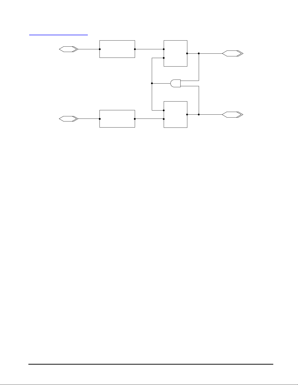
Freescale Semiconductor, Inc.
MC145181
nc...
I
cale Semiconductor,
Frees
查询"MC145181"供应商
Figure 34. Phase Frequency Detector Logic Diagram
PG1
Ref
Pulse Generator
PG2
In
Pulse Generator
The behavioral model of the phase frequency detector
shown in Figure 35 is derived using the phase frequency
detector logic diagram. Behavioral models for the pulse
generator, AND gate (Figure 36), and RS flip–flops
(Figure 37) are created using analog behavioral blocks. The
pulse generator is created using a delay block and a “gate”
defined by the behavioral expression:
If [V(v1) ≥ 1 & V(v2) , 1, 5, 0]
v1 and v2 represent the two inputs to the block.
This is the behavioral expression for an AND gate with one
input inverted. The addition of the delay element produces a
pulse whose width equals the delay element.
The pulses appearing at the output of HB1 and HB2
(Figure 35) are used to set the flip–flops, RSFF1, and
RSFF2. The leading pulse will set the appropriate flip–flop
resulting in a high at the output of that flip–flop. The output of
this flip–flop will remain high until the arrival of the second (or
lagging) pulse sets the second RS flip–flop. The presence of
a high on both RS flip–flop outputs results in the generation of
the reset pulse. The reset pulse is generated by the analog
behavioral block (configured as an AND gate) and the delay
element. The delay element is necessary to eliminate the
zero delay paradox of input to output to input.
The output of the phase frequency detector is two pulse
trains appearing at Rφ and Vφ. When the PLL is locked, the
pulses in both pulse trains will be of minimum width. When
the phase frequency detector is out of lock, one pulse train
will consist of pulses of minimum width while the width of the
pulses in the second train will be equal to the lead/lag
relationship of the input signals. If the Ref input leads ‘In’, the
pulse train at Rφ will consist of pulses whose width equals the
lead of Ref. If Ref lags ‘In’, the width of the pulses appearing
at Vφ will equal this lag.
OutIn
OutIn
RSFF1
S
P1
R
RSFF2
R
P1
S
The terms lead and lag used in this explanation represent
an occurrence in time rather than a phase relationship. At any
condition other than locked, one input (either In or Ref), will
be of a higher frequency. This results in the arrival of the
pulse at that input ahead of the pulse at the other input, or
leading. The second then is lagging.
To simulate the operation of the phase frequency detector
in an actual circuit, a charge pump needs to be added. The
behavioral model for this is shown in Figure 38. Two
voltage–to–current behavioral models are used to produce
the charge pump output. Two voltage–controlled switches
with additional behavioral models, monitor the voltage of the
output of the charge pump and clamp to 0 or VCC to simulate
a real circuit.
T o ensure the model conforms to the PLL, the delay blocks
in the phase frequency detector should be set to the
expected value as specified by the MC145181 data sheet. In
addition, the charge pump sink and source current behavioral
model should also be set to deliver the desired current and
VCC specified to ensure correct clamping.
Modeling the VCO
The VCO (Figure 39) is also modeled using Analog
Behavioral Modeling (ABM). The model used in the following
examples assumes a linear response; however, the control
voltage equation can be modified as desired. The circuit is
modeled as a sine generator controlled by the control
voltage. The sine generator can be modeled using the
EVALUE function or the ABM function. In Figure 39, the
EVALUE function is used to generate the divided output and
the ABM function is used for the undivided output. Either the
GVALUE or the ABM/I function can be used for the control
voltage.
R
φ
V
φ
MOTOROLA RF/IF DEVICE DATA
For More Information On This Product,
Go to: www.freescale.com
37
Page 38

Freescale Semiconductor, Inc.
MC145181
查询"MC145181"供应商
Figure 35. Behavioral Model of the Phase Frequency Detector
HB1
V1
Delay
Ref
In
nc...
I
In Out
Pulse Generator
Delay
In Out
Pulse Generator
V2
HB2
V2
V1
Out
Out
Delay
Out
In
RSFF1
S
P1
R
If [V(Q1)>=1 & V(Q2)>=1, 5, 0]
RSFF2
R
P1
S
R
φ
V
φ
cale Semiconductor,
Frees
Figure 36. Behavioral Block Used for the
Pulse Generator
v1
v2
Figure 37. Behavioral Block Used as an RS Flip–flop
S
R
In1
In2
v1
v2
In3
If (V(v1) ≥ 1 | V(v2) < 1, 5, 0)
Out
If [V(In1)>=1 & V(In2)<1 | V(In2)<1, 5]
If [V(In2)>=1, 0]
If [V(In3)>=1 & V(In2)<1, 5, 0]
Q
out
38
If [V(Q)>=1, 5, 0]
For More Information On This Product,
Go to: www.freescale.com
MOTOROLA RF/IF DEVICE DATA
Page 39

Freescale Semiconductor, Inc.
MC145181
查询"MC145181"供应商
Figure 38. Charge Pump Model
If [V(In1)>=1 j V(In2)<1, 1 x 10⁻³, 0]
R
φ
V
φ
nc...
I
In1
In2
If [V(In2)>=1 j V(In1)<1, 1 x 10⁻³, 0]
If [V(idrive) > 0, 0, 1]
If [V(idrive) < 5, 0, 1]
S1
+
–
0
S2
+
–
0
+
–
+
–
Sbreak
+
5
–
0
0
Sbreak
0
V1
0
idrive
PD
out
cale Semiconductor,
Frees
Parameters:
6.283
t
w
f
250 x 10
c
k1
525 x 10
Parameters:
N
5000
Q
1 x 10
c
ctrl
–6
Figure 39. VCO Behavioral Model
0
IC = 0
int
1 x 10
VCO
1 x 10
–6
out
R1
5 V
0 V
1 x 10
Out
99
3
1
6
6
sin {tw [fc time + N v(int)]}
E1
ctrl
In+
In–
evalue
sin t
In+
In–
gvalue
k1
tw N
Out+
Out–
f
c
ƪƫ
time + v(int)
w
N
G1
v(ctrl) Q
c
+
C1
MOTOROLA RF/IF DEVICE DATA
For More Information On This Product,
Go to: www.freescale.com
39
Page 40

nc...
I
cale Semiconductor,
Frees
Freescale Semiconductor, Inc.
The equation for the sine generator is:
f
查询"MC145181"供应商
fc is defined as the output frequency when the control voltage
is 0. This is the expected VCO frequency before frequency
division. For the purpose of simulation, the counter value, N,
has been written into the equation to ensure the correlation
between the modeled circuit and the mathematical loop filter
calculations. tw is 2π; additional decimal places can be added
as needed. v(int) is the control voltage effect and is defined in
these examples as:
where k1 is the VCO gain in rad/V.
The value C1 in the schematic of the VCO can be
arbitrarily changed; however, the value must match that of
Qc. Qc determines the value of the current to be integrated by
the capacitor C1. R1 is arbitrarily set to 1 x 1099 and is not an
active part of the circuit; however, it must be included to
prevent open pin errors from the PSpice software. The
GVALUE function is used to perform the generation of v(int).
There is some interaction between the integrator, (GVALUE
output and C1) and R1. V(int) is a continuous ramp that is
loaded by the resistance of R1. Unless the GVALUE output
current is sufficiently large for the value chosen for R1, the
VCO control voltage required to maintain lock will increase
throughout the simulation producing nonlinear operation.
Modifications to the circuit can be performed either by
changing the values in the parameter list or for major
changes to the VCO characteristics, the equations for the
sine generator, or control voltage can be altered.
The output of the sine generator is amplified by 1000 to
produce a sharp rise/fall time and the output limited to swing
between the values of 0 V and 5 V to convert it to a digital
output. The resultant circuit/symbol accepts a voltage input
from the loop filter and produces a square wave output at the
HB2
In
V1
+
–
Ref
ƪ
w
k1
twN
c
time + v(int) .e = sin t
N
v(cntl) 1 x 10⁻⁶ .v(int) =
R
φ
V
φ
MC145181
ƫ
Figure 40. PLL Closed Loop Model
HB1
R
φ
PD
V
φ
out
R1
desired frequency. This frequency should be chosen to
represent the frequency present at the output of the N
counter of the PLL frequency synthesizer.
The second output represented by the ABM function is a
sine wave output of the frequency expected from the actual
VCO. The primary purpose of this output is to allow full
frequency simulation for spectrum analysis. By running a
transient analysis of sufficient time, it is possible to determine
spur content and level. If sufficient resolution is used in the
simulation, the PSpice probe FFT transform can be used to
provide the typical spectrum analyzer display.
Loop Filter Simulation
The circuit shown in Figure 40 is used to simulate the
closed loop operation for a single charge pump output.
Component values for the loop filter should be computed
using information from the previous section. Initial conditions
can be set using the “IC1” symbol with starting values
specifying the initial condition.
By adjusting component values for the loop filter,
performance of the closed loop operation can be monitored.
The control voltage to the input of the VCO can be monitored
for a variety of conditions including settling time, lock time,
and ripple present at the VCO input. In addition, the output of
the VCO can be monitored for spur sidebands caused by
ripple on the loop filter output; however, expected operation
at high frequencies may be difficult due to the excessive data
that can be generated.
As the divider ratio, N, increases for a fixed step
frequency, the number of data points required to obtain
sufficient information to overcome aliasing problems may
become excessively large. In addition, the number of
samples required should be three or more per cycle. For
VCO frequencies in the range of 500 MHz, this means the
step ceiling needs to be in the range of 100 to 500 ps. If a
simulation time of 1 ms is needed, the actual computer time
can be several hours with data accumulation in the 1– to
2–Gbyte range.
ctrl
VCO
U3
out
Out
+ +
IC = 3.5
R3
C2C3
7.5 k
75 k
0.2 n2 n
C1
00
IC = 3.5
0.1 n
0
1 kR4
40
0
0
For More Information On This Product,
Go to: www.freescale.com
MOTOROLA RF/IF DEVICE DATA
Page 41

Freescale Semiconductor, Inc.
7C. MAIN LOOP FILTER DESIGN — ADAPT
Introduction
查询"MC145181"供应商
For PSpice simulation, the schematic model shown in
Figure 41 was chosen. The classical PLL model employing a
phase–frequency detector, a VCO, and an adaptive loop filter
is used to simplify visualization of circuit operation. The
parameter tables allow for modification of circuit performance
by providing an easy method for altering critical values
without necessitating changes to sub–level schematics. The
definition for the terms are:
tw =2π,
fr = reference frequency,
td = time delay; allows delay of the start of the high
current mode (used to perform reference spur
measurements),
CPL = charge pump low current,
CPH = charge pump high current,
N = N counter value,
nc...
I
MC145181
Sz = amount the N counter is being increased (or
decreased) by,
St = number of fr cycles that CPH is active; this value
is either 16, 32, 64, or 128,
VCPHH = charge pump voltage – high,
VCPHL = charge pump voltage – low,
K1 = VCO gain (Hz/volt),
fc = VCO frequency at 0 V control voltage,
H = reference spur scaling factor.
Modeling the Phase–frequency Detector
Figure 42 is a schematic of the phase–frequency detector.
It includes the reference oscillator model, phase–frequency
detector model, and charge pump models. V1 is the control
element used to generate the step time for switching between
CPL and CPH. The signal source VPULSE, is used to
simulate the timer that controls when CPL and CPH are
turned on. PW calculates the pulse width that simulates the
counter from the values for St and fr that are entered in the
parameter tables on the top level schematic.
Figure 41. T op Level PLL Model
cale Semiconductor,
Frees
Parameters:
6.283185308
t
w
f
25 k
r
H
1
Parameters:
N
29320
S
400
z
S
32
t
Parameters:
CPL
1 x 10
CPH
4 x 10
K1
4 x 10
Parameters:
VCPHH
VCPHL
f
Parameters:
t
5
0
727.6 x 10
c
0
d
–3
–3
6
HB1
fr N – f
IC =
HB2
PD
–Lo
out
In
PD
–Hi
out
6
Figure 42. Phase–frequency Detector with Dual Charge Pumps
In
HB1
+
60.4 k R1
20 k
HB3 HB2
f
in
c
K1
40.2 k
C1
330 p
fr N – f
IC =
+
C5
+
IC =
C6
R
φ
c
K1
C2
330 p
330 p C3
fr N – f
c
K1
10%
3300 p
0
R2
R
+
PD
φ
fr N – f
K1
50 p
0
c
VCO
PD
ctrl
out
–Lo
Out
1 kR10
0
IC =
C4
33 pR3
0
–Lo
out
Shift
S
t
PW =
4 f
r
+
–
4 t
d
td =
f
r
MOTOROLA RF/IF DEVICE DATA
PD
Shift
out
–Hi
Shift
RefRef
V1
0
V
φ
V
φ
For More Information On This Product,
Go to: www.freescale.com
PD
out
–Hi
41
Page 42

Freescale Semiconductor, Inc.
Reference Oscillator
The reference oscillator is shown in Figure 43. The
查询"MC145181"供应商
oscillator is modeled using an analog behavioral block. The
function for the block is written as an “If” condition. If the
signal shift is low, the reference frequency fr will be generated
if shift is high, a signal of four times fr will be generated. The
limiter/gain block converts the low level sine wave output of
the analog behavioral block into a square wave. The values
of 0 for the low value and 5 for the high value are used
throughout. These values are chosen out of habit and are not
critical in an analog behavioral environment, providing the
conformity is universal throughout the design.
Figure 43. Reference Oscillator
Shift
nc...
I
Phase–frequency Detector
The actual phase–frequency detector model minus
reference oscillator and charge pumps is shown in Figure 44.
The detector is composed of three delay modules: a
behavioral AND gate, and two RS flip–flops. The STP
function resets the phase/frequency detector logic on
initiation of the simulator. The circuit for the behavioral RS
flip–flop is shown in Figure 45.
Shift
If [V(shift) < 1, sin (tw fr time), sin (tw fr time) 4]
Ref
cale Semiconductor,
MC145181
The RS flip–flop equation illustrates the benefit of using
the behavioral block instead of using a primitive logic
element. A delay block and the behavioral gate equation
generate a pulse whose width is equal to the value of the
delay block. To generate the output using a primitive logic
element such as a NAND gate, an inverter would be
necessary to invert one of the NAND inputs. This approach
requires three elements to be used instead of the two of the
behavioral approach just for the pulse generator. In the
behavioral approach, the equation for the behavioral AND
gate is folded into the RS flip–flop, eliminating a separate
gate altogether. Constructing the model with classic logic
elements would require two NOR gates for the flip–flop, a
delay element, an inverter, and an AND gate; five elements
as compared with three for the behavioral approach. Since
the RS flip–flop is used in two places in the model, four less
components are needed for simulation. Since the speed of
the simulation is directly impacted by the number of
components being simulated, any reduction in the total
5 V
HB1
In1
In2
Ref
Q
out
1 k
0 V
Figure 44. Phase–frequency Detector Logic
number of components is a savings in simulation time and
computer memory .
The RS flip–flops generate the lead or lag outputs that are
used to “steer” the VCO. The pulse generator equation
produces narrow pulses coincident with the leading edge of
each of the input signals. These pulses set the appropriate
RS flip–flop. Once set, the leading flip–flop must wait until the
lagging flip–flop is also set. The behavioral AND gate
provides the necessary output pulse to reset the flip–flops.
The delay element placed at the output of the behavioral
AND gate prevents an undefined state for the detector. The
value 5 ns is chosen to correspond with the data sheet. The
logic functions as a three state phase/frequency detector with
an operating range of ±2π. Rφ and Vφ deliver positive pulses,
whose width represents the amount of the lead of each input
over the other input.
Q1
R
φ
If [V(Q1)>=1 & V(Q2)>=1 | V(delay)>=1, 5, 0]
Frees
42
Delay
5 ns
HB2
In1
Q
In
5 STP (5 ns – Time)
out
In2
Q2
Delay
V
φ
For More Information On This Product,
Go to: www.freescale.com
MOTOROLA RF/IF DEVICE DATA
Page 43

Freescale Semiconductor, Inc.
MC145181
nc...
I
cale Semiconductor,
Frees
查询"MC145181"供应商
Figure 45. Behavioral RS Flip–flop
U1
In1
In2
Charge Pump Model
The schematic used for the charge pump in the
phase–frequency detector model is shown in Figure 46. Each
charge pump is made from two analog behavioral blocks.
The blocks chosen are three input behavioral blocks with
current outputs. The two blocks are connected in push–pull
to generate the appropriate source and sink output. The
output of each block is defined using an “If” statement to
monitor the input signals and generate the correct output at
the appropriate time.
One note about this type of design. SPICE does not limit
the output voltage swing necessary to generate the
programmed current. It is possible to implement values for
the loop filter, which will cause the charge pump to exceed
the rail voltage. To limit the output voltage to prevent
exceeding the value of the rails, the two behavioral blocks,
voltage–controlled switches S1 and S2, and constants
VCPHH and VCPHL are added. S1 and S2 on/off resistance
is set to 1 Ω and 1 x 10¹² Ω, and the off/on voltage is set to
0 V and 1 V to correspond to the behavioral blocks. The
values defined by the constants are accessible from the
parameter tables on the top level schematic.
VCO Model
The model used for simulating the VCO is shown in
Figure 47. The VCO is composed of a sine wave generator
and a control element. An analog behavioral block is used as
a sine wave generator and a GVALUE element is used as a
control element. The GVALUE is operated as an integrator.
The output of the integrator is defined as
v(int) = k1 v(ctrl) Qc .
The block designated to provide the feedback to the
phase–frequency detector uses a single input analog
behavioral block. The signal shift generated by V1 in the
phase–frequency detector block is used to define the output
frequency of the behavioral block. In this manner, the
switching of the N and R values for the programmable
counters can be simulated. In the implementation shown, the
two frequencies will be either 25 kHz or 100 kHz when locked
to the reference oscillator.
V1 V2
In2
Delay
1 ns
If [V(v1)>=1 & V(v2)<1 & V(In2)<1, 5]
If [V(In2)>=1, 0]
If [V(In3)>=1 & V(In2)<1, 5, 0]
Q
In3
If [V(Q)>=1, 5, 0]
The other behavioral block is used to generate a VCO
output dependent on the loop, but not contributing to the
operation of the loop. This is used to emulate the actual VCO
output with one modification. “H” has been added to the
equation generating the sine wave. If H is defined as 1, the
sine wave generated will be the same as the expected VCO
output. If H is chosen as some value greater than 1, the
frequency of the output will be reduced accordingly. This is
useful when running simulations designed to show reference
spur levels.
In cases where it is desirable to view reference spur levels,
simulation can become difficult or impossible. For example,
consider the circuit that is being discussed. This circuit
represents the evaluation kit (MC145230EVK) using a VCO
tunable between 733 MHz to 742 MHz, with a step frequency
of 25 kHz.
NOTE
This example is for reference only. The
maximum operating frequency of the MC145181
is 550 MHz. Operation of the VCO at
frequencies greater than 550 MHz requires the
inclusion of additional external division such as a
prescaler.
To obtain useful information from the simulation, a
sampling rate greater than the Nyquist limit must be used
(three to five samples per cycle). This dictates a step size
less than 1/2 nanosecond. Additionally, the reference
frequency is only 25 kHz. To accurately represent the
conditions for spur generation, the simulation time must be
long enough to include a sufficient number of fr periods.
Otherwise, no spurs are generated. In addition, the data file
system is limited to 2 Gbyte, either in the NT 4.0 operating
system or in PSpice itself. If the file exceeds 2 Gbyte, the
data is discarded. To simulate reference spur generation at
730 MHz, a 1 ms simulation time was chosen. The simulation
ran for several hours and generated a data file just under
2 Gbyte. The result is shown in Figure 48. The plot obtained
from the EVK is shown in Figure 49 for comparison.
Q
out
MOTOROLA RF/IF DEVICE DATA
For More Information On This Product,
Go to: www.freescale.com
43
Page 44

Freescale Semiconductor, Inc.
MC145181
查询"MC145181"供应商
Figure 46. CPL and CPH Charge Pumps
V
φ
R
φ
Shift
nc...
I
In1
In2
Shift
If [V(In1)>=1 & V(In2) <1 & V(shift) <1, CPL, 0]
0
0
If [V(In2)>=1 & V(In1) <1 & V(shift) <1, CPL, 0]
If [V(In1)>=1 & V(In2) <1 & V(shift) >= 1, CPH, 0]
0
drv
0
If (V(In2)>=1 & V(In1)<1 & V(shift) >= 1, CPH, 0)
PD
PD
out
out
–Lo
–Hi
cale Semiconductor,
Frees
If [V(idrv) > VCPHH, 1, 0]
If [V(drv) < VCJPHL, 1, 0]
Sbreak
0
VCPHH
S4
+
–+–
0
S5
+
–+–
VCPHL
44
For More Information On This Product,
Go to: www.freescale.com
MOTOROLA RF/IF DEVICE DATA
Page 45

Freescale Semiconductor, Inc.
MC145181
查询"MC145181"供应商
Figure 47. VCO Model
Parameters:
Qc1 x 10
Shift
nc...
I
–6
If (V(turbo) <1, sin
Turbo
ctrl
fc time + v(int)
ǒǓƪƫ
sin t
w
t
w
ǒǓƪƫ
ǒǓƪƫ
sin
N + S
4 t
N + S
w
fc time + v(int)
z
fc time + v(int)
z
ctrl
,
G1
In+
In–
gvalue
0
K1 v(ctrl) Q
VCO
H
5 V
0 V
6
1 x 10
+
IC = 0
int
–6
C1
c
R11 x 10
1 x 10
99
Out
cale Semiconductor,
Frees
Figure 48. Reference Spur Simulation at 730 MHz
MOTOROLA RF/IF DEVICE DATA
For More Information On This Product,
Go to: www.freescale.com
45
Page 46

Freescale Semiconductor, Inc.
MC145181
查询"MC145181"供应商
Ref Lvl – 73.32 dB
10
–0
–10
–20
–30
1AVG 1SA
–40
–50
–60
nc...
I
–70
–80
–90
Figure 49. Sybil EVK Reference Spur Measurements
25.00000000 MHz10 dBm
SWT 130 ms Unit dBm
1
1
cale Semiconductor,
Frees
–100
–110
Center 737.5000009 MHz Span 64 kHz
It should be noted that the reference spur values obtained
from the simulation are lower than the values obtained from
the actual EVK. This is because the simulation model is an
“ideal” modeling of the PLL. To obtain results closer to the
actual implementation, the models should be “massaged” to
be more representative of the actual circuit. For example,
spur levels more consistent with actual circuitry can be
obtained by adding a resistance to ground at the input of the
VCO to represent leakage. The value chosen should be
consistent with VCO and circuit component performance.
To reduce simulation time, the H value may be used. By
reducing the frequency of the VCO output, the number of
samples required for simulation can also be reduced. The
output shown in Figure 50 shows the result of dividing the
VCO output of 730 MHz by 7.3 to produce a 100 MHz output.
The reference spurs are better represented since adequate
simulation time is possible.
To generate these outputs, the parameter values used
were those shown on the top level schematic. The simulator
was set to run a transient sweep, with td set for a delay that
would prevent the 4X frequency from being started. The initial
conditions were set to 1 V and the simulation run for 1 ms.
VCO was monitored and the probe display button FFT was
initiated. The X and Y axis were adjusted to those shown.
Note: These simulations are presented as the result of
“ideal” models and may not accurately display real hardware.
It would be best to load the VCO input with additional leakage
devices such as a large resistance, to accurately display real
6.4 kHz
conditions. These models are starting points for more
accurate implementations.
Loop filter analysis is more accurate, since the
predominate factors are in the loop filter itself. T o simulate the
performance of the loop filter, td is set for 0, N is set to the
desired divider value, and Sz is set to the desired step. For
this example, 733 MHz was chosen.
NOTE
These values are for reference only. The
maximum operating frequency of the MC145181
is 550 MHz. For VCO frequencies greater than
550 MHz, an added external divider such as a
prescaler is necessary.
With the VCO model shown, V(ctrl) = 0 produces an output
of 727.6 MHz and at V(ctrl) = 1.35 V, the VCO frequency
would be 733 MHz; the minimum MC145230EVK default
operating frequency . T o show the response of the loop filter to
a 10 MHz step at this operating frequency, Sz = 10 MHz /
25 kHz = 400. The simulation is run for 1 ms with a step
ceiling of 100 ns. The result is shown in Figure 51.
If the simulation is examined over a longer period of time,
the long term settling can be compared to the performance of
the actual circuitry. The plot shown in Figure 52 shows the
VCO control voltage with the display resolution set to 1 mV.
This compares to the plot of frequency variation
measurements made on the actual EVK. This plot is shown in
Figure 53.
46
For More Information On This Product,
Go to: www.freescale.com
MOTOROLA RF/IF DEVICE DATA
Page 47

Freescale Semiconductor, Inc.
MC145181
查询"MC145181"供应商
nc...
I
Figure 50. H Set to Generate a 100 MHz Output
cale Semiconductor,
Frees
Figure 51. 10 MHz Step for an Operating Frequency of 729 MHz
MOTOROLA RF/IF DEVICE DATA
For More Information On This Product,
Go to: www.freescale.com
47
Page 48

Freescale Semiconductor, Inc.
MC145181
查询"MC145181"供应商
Figure 52. VCO Settling
nc...
I
Figure 53. Frequency Settling of the EVK
cale Semiconductor,
Frees
Freq C tlk only
waiting for trigger
742.003715MHz
741.999715MHz
741.995715MHz
0.00 s
µ
s
T 742.2
1
T 0.00s
2
1.000 ms
200.0 µs/div
∆
–742.2 µs
2.0000 ms
VERTICAL
Center/
Span
Center
741.999715M
Span
1.000k /div
Find Center
Find Center
And Span
Top/
Bottom
8.000k
H
Z
H
Z
H
Z
48
For More Information On This Product,
Go to: www.freescale.com
ref int
MOTOROLA RF/IF DEVICE DATA
Page 49

Freescale Semiconductor, Inc.
It is noted that the results obtained from the simulation
compare favorably to those obtained from the measurements
查询"MC145181"供应商
of the EVK. The simulation display resolution is adjusted to
represent the same ±4 kHz deviation as shown in Figure 53.
Since variation in VCO control voltage is equal to the VCO
frequency divided by the VCO gain, this axis may be
redefined to show change in frequency rather than change in
control voltage.
The models shown represent a “skeleton” that may be
used to develop extensive and reliable simulations that can
greatly reduce actual breadboarding and testing. In addition
to the basic simulations shown, PSpice provides a method by
which worst case and Monte Carlo evaluation can be
nc...
I
MC145181
performed on all, or selected components. By limiting the
circuit to minimum necessary components, simulation can be
performed using only the PSpice evaluation copy . In addition,
the optional PSpice program Optimizer should allow refining
the loop filter more easily .
While PSpice is a powerful tool, it is not without limits.
Since it was designed to run on large mainframe computers,
the PC is just now becoming powerful enough to make use of
the capability of the simulator. A fast Pentium class processor
with a large RAM and a hard drive of the Gbyte size is a
necessity. Even with the most judicious planning, some
simulations will “bump” the limits of the system.
cale Semiconductor,
Frees
MOTOROLA RF/IF DEVICE DATA
For More Information On This Product,
Go to: www.freescale.com
49
Page 50

nc...
I
cale Semiconductor,
Frees
Freescale Semiconductor, Inc.
7D. SECONDARY LOOP FILTER DESIGN
Low Pass Filter Design for PD
查询"MC145181"供应商
The design of low pass filtering for PD
can be accomplished using the following design information.
In addition to the example included here, Motorola
Application Note AN1207, also includes examples of active
filtering which may be used to supplement this information.
PD
out
R
1
ωn =
ζ = 0.5 ω
F(s) =
Definitions:
N = Total Division Ratio in Feedback Loop
Kφ (Phase Detector Gain) = VDD/4π V/radian for PD
Kφ (Phase Detector Gain) = VDD/2π V/radian for φV
K
(VCO Gain) =
VCO
For a nominal design starting point, the user might consider a
damping factor ζ ≈ 0.7 and a natural loop frequency ωn ≈
(2πfR/ 50), where fR is the frequency at the phase detector
input. Larger ωn values result in faster loop lock times and, for
similar sideband filtering, higher fR–related VCO sidebands.
Recommended Reading:
Gardner, Floyd M.,
edition).
and Design (second edition).
1980.
Coherent Receiver Design.
1976.
New York, Wiley–Interscience, 1981.
Theory and Design.
1983.
Circuits, with Experiments.
and Co., 1978.
Ridge Summit, P A, Tab Books, 1980.
New York, Wiley–Interscience, 1979.
Manassewitsch, Vadim,
Blanchard, Alain,
Egan, William F.,
Rohde, Ulrich L.,
Berlin, Howard M.,
Kinley, Harold,
The PLL Synthesizer Cookbook.
NC(R1 + R2)
R2C +
ǒ
n
(R1 + R2)sC + 1
Phaselock Techniques (second
Frequency Synthesizers: Theory
Phase–Locked Loops: Application to
New York, Wiley–Interscience,
Frequency Synthesis by Phase Lock.
Digital PLL Frequency Synthesizers
Englewood Cliffs, NJ, Prentice–Hall,
Design of Phase–Locked Loop
Indianapolis, Howard W. Sams
i
out
R
2
C
KφK
VCO
KφK
R2sC + 1
and φ
R
2π∆f
∆V
New York, Wiley–Interscience,
out
VCO
N
VCO
VCO
VCO
i
for the device
Ǔ
out
Blue
MC145181
i
Seidman, Arthur H.,
Handbook
& Sons.
Programmable Calculator,”
Motorola Semiconductor Products, Inc., 1970.
Semiconductor Products, Inc., Reprinted with permission
from
Motorola Semiconductor Products, Inc., 1992.
Semiconductor Products, Inc., 1998.
Example:
throughout the range used in this example. The gain for the
VCO has been given as 3.4 MHz/V and is multiplied by
2π rad/s/Hz for calculating loop filter values.
K
VCO
The gain for the phase detector is defined as
Using a value for VDD (phase detector supply voltage) of
3.6 V with the output voltage multiplier turned off, the value is
Let
and
With a damping factor of 0.707,
does impact the performance of the loop filter. If possible, a
range of choices for C should be used to calculate potential
loop filters and the resultant filters simulated, as will be
shown below, to determine the best balance.
, Chapter 17, pp. 538–586. New York, John Wiley
Fadrhons, Jan, “Design and Analyze PLLs on a
AN535, Phase–Locked Loop Design Fundamentals,
AR254, Phase–Locked Loop Design Articles, Motorola
Electronic Design,
AN1207, The MC145170 in Basic HF and VHF Oscillators,
AN1671, MC145170 PSpice Modeling Kit, Motorola
Given the following information:
VCO frequency = 45.555 MHz,
Frequency step size = 5 kHz,
VCO gain = 3.4 MHz/V.
Design a loop filter with a damping factor of 0.707.
The VCO is assumed to have a linear response
= 2π rad/s/Hz x 3.4 MHz/V = 2.136 x 10⁷ rad/s/V .
Kφ =
Kφ = = 0.2865 V/rad .
ωn = = 628.3 rad/s
F
N = = 91 11 .
Choosing C = 0.05 µF and calculating R1 + R2,
R1 = (R2 + R1) – R2 = 34 k – 15 k = 19 kΩ 20 kΩ .
The choice for C is somewhat arbitrary, however, its value
VCO
F
step size
R1 + R2 = = 34 kΩ .
0.707
0.5 ω
R2 =
Integrated Circuits Applications
EDN
. March 5, 1980.
1987.
V
DD
V/rad for PD
4π
3.6
4π
2π f
r
50
45.555 MHz
=
Kφ K
N C ω
–
Kφ K
n
C
5 kHz
VCO
n
N
2
VCO
i
.
out
= 15 kΩ ,
50
For More Information On This Product,
Go to: www.freescale.com
MOTOROLA RF/IF DEVICE DATA
Page 51

nc...
I
cale Semiconductor,
Frees
Freescale Semiconductor, Inc.
If additional filtering is desired, R1 may be split into two
equal resistors and a capacitor to ground inserted. Since the
查询"MC145181"供应商
closest resistance to one–half of 9 k is 4.7 kΩ , this value is
chosen for R1a and R1b. The maximum value for the added
capacitance is based on the bandwidth of the original loop
filter.
The general form for the transfer function for the passive
filter shown in Figure 54, can be shown to have the form:
s + ω
F(s) = K
where
ω1 = ,
ω3 =
ƪ
where
and
Since splitting R1 into two equal values, R1a and R1b, and
inserting the capacitance between the junction of R1a and
R1b does not change the position of the pole located at ω1,
the value of ω1 remains
ω1 = . =
(R1a + R1b + R2) C
The 0 identified at ω2 = 1/R2 C is also unaffected by the
addition of Cc if ω3 > ω2.
Since
the value of Cc can be determined by specifying the value for
ω3 and using the values already determined for R1 and R2.
The rule of thumb is to choose ω3 to be 10 x ωB so as not to
impact the original filter. ωB can be found as
ωB = 628.3 rad/s
+
= 1.293 x 10³ rad/s .
10 ωB = 12.93 x 10³ rad/s .
The circuit for the passive loop filter is shown in Figure 54.
R1 is split into two equal values and Cc inserted at the
ƪ
h
(s + ω1) (s + ω3)
(R1a + R1b + R2) C
ω2 = ,
R2C
1
R1a R1b + R1a R2
(R1 + R2)
R1 = R1a + R1
ω3 > ω2 .
1
R1a = R1b = .
(2+ 4 (0.707)2 + 4 (0.707)4)]
2
1
1
b
(R1 + R2) C
R1
2
(2 + 4ζ2 + 4ζ4)]ωB = ωn [1 + 2ζ2 +
[1 + 2 (0.707)
MC145181
ƫ
,
ƫ
C
c
1
2
junction of R1a and R1b. Using the values defined above, C
is determined to be
Cc =
R1a R1b + R1a R2
ƪ
=
R1a R1b + R1a R2
ƪ
Figure 54. Passive Loop Filter for PD
V1
0
Open Loop AC Analysis of the Loop Filter
AC analysis is chosen for the mode of simulation for
PSpice and VSIN is chosen for V1 and is set to produce a 1 V
peak output signal. The simulation is then run and the result
shown in Figure 55.
A Bode plot of the loop filter is obtained which describes
the open loop characteristics of the loop filter. The corner
frequencies of the filter can be modified and the simulation
rerun until the desired wave shape is obtained. Since AC
analysis runs much faster than transient analysis, the AC
open loop analysis of the loop filter is much quicker and
requires less resources than the closed loop transient
analysis.
Closed Loop Filter Simulations Using PSpice
The top level schematic for simulating a simple loop filter
for PD
filter uses the values calculated above.
internal phase detector, PD
above, and a VCO. The parameter table allows altering the
divider value of N, the maximum current obtained from
PD
schematic.
behavioral modeling is used rather than discrete transistor
modeling to reduce component count and improve simulation
efficiency .
transforms the input ctrl into the voltage control V(int) and a
sine wave generator function whose frequency is controlled
by V(int). EVALUE and GVALUE functions are used to
perform the transforms. The analog behavioral models, ABM
and ABMI, can also be used.
i
operating closed loop, is shown in Figure 56. This
out
The schematic represents the PLL function using the
i
, and PD
out
The schematic for the VCO is shown in Figure 57. Analog
The behavioral VCO is composed of an integrator that
1
ƫ
ω
(R1 + R2) ω
(R1 + R2) 10
R1
a
10 k
out
3
1
C
c
charge pump voltage from the top level
3
= 10.83 nfd 10 nfd
.
ƫ
ω
B
R1
b
10 n
0
10 k
R2
C
i
, the loop filter calculated
out
+
out
15 k
50 n
0
i
IC = 0
V
c
MOTOROLA RF/IF DEVICE DATA
For More Information On This Product,
Go to: www.freescale.com
51
Page 52

Freescale Semiconductor, Inc.
MC145181
查询"MC145181"供应商
Figure 55. Bode Plot of the Passive Loop Filter
nc...
I
cale Semiconductor,
Frees
Parameters:
CPN0.3 mA
9111
Parameters:
VCPH
VCPL
3.6
0
Figure 56. Passive Loop Filter
HB1
15 k
50 nf
0
V
Ctrl
+
IC = 0
Out
+
C4
IC = 0
10 nf
0
R6
10 k
R2
C2
HB2
Ref
PD
V2
+
–
0
In
out
R1
10 k
52
For More Information On This Product,
Go to: www.freescale.com
MOTOROLA RF/IF DEVICE DATA
Page 53

Freescale Semiconductor, Inc.
MC145181
nc...
I
cale Semiconductor,
Frees
查询"MC145181"供应商
Figure 57. VCO Behavioral Model
ctrl
E1
In+
In–
evalue
sin t
G1
In+
In–
gvalue
k1
ǒǓ
tw N
w
v(ctrl) Q
Parameters:
6.283
t
w
f
38.756 x 10
c
K1
21.36283005 x 10
Parameters:
Qc1 x 10
G1 performs the operation [k1/(tw N)] v(ctrl) Qc. This
integrates the input ctrl to produce a voltage ramp used by E1
to produce the desired output. This input is integrated by C1
whose value should equal Qc for most applications. R1 is
required by SPICE to prevent a floating node error.
E1 performs the calculations necessary to generate a sine
wave of the desired frequency based on the values listed in
the parameter tables and the value of ctrl. The output of E1 is
multiplied by 1 x 10⁶ and limited to 0 and 5 to obtain a square
wave with a fast rise/fall time. Since I/O_STM is a standard
model whose values are 0 and 5, these are used here and in
the phase detector rather than modifying the component
libraries.
The parameter tables provide a convenient method for
setting VCO parameters. tw is 2π, fc is the zero control
voltage VCO frequency, and K1 is the VCO gain in rad/s/V.
The sub–schematic for the phase/frequency detector
section of the drawing is shown in Figure 58. This is
composed of two blocks, HB3 and HB4. HB3 performs the
PD
i
function with HB4 performing the actual phase
out
detector operation.
The circuit for the phase/frequency detector is shown in
Figure 59. The model is made up of two pulse generators,
two RS flip–flops, and appropriate behavioral gates.
HB1 and HB2 are RS flip–flops. These are constructed
from behavioral blocks as shown in Figure 60. A behavioral
AND gate with a 5 ns delay completes the three state (±2π)
phase/frequency detector. The STP function ensures the RS
flip–flops are reset at initiation.
To perform the phase detector function, the Ref and f
inputs of the behavioral RS flip–flops are configured to
simulate edge triggered operation. This is achieved by
placing a 1 ns delay in the Ref and fin signal paths. The input
and output of the delay are compared by the input behavioral
block and interpreted as a 1 ns pulse. These pulses are used
to set HB1 and HB2. If fin leads Ref, the In flip–flop, HB2, will
be set first. When Ref leads fin, the Ref flip–flop, HB1, will be
set first. The lagging edge drives the second flip–flop output
high and the behavioral AND gate then resets both flip–flops.
The delay line at the output of the behavioral AND gate
prevents PSpice from being confused and also completes
the simulation of the phase detector. The outputs of the two
RS flip=flops are labeled Rφ and Vφ. The time between the
6
6
–6
ctrl
0
IC = 0
1 x 10
5 V
0 V
int
–6
i
, either a model of the transistors used for
out
Out+
Out–
f
c
ǒǓƪƫ
time + v(int)
N
+
C1
c
leading and lagging edges is reflected in the pulse width of
the leading edge flip–flop. The lagging edge flip–flop will
display a narrow pulse equal in width to the value chosen for
the delay at the output of the behavioral AND gate. This
should be programmed to the minimum value as specified by
the data sheet and is usually 5 ns or less.
Since the outputs Rφ and Vφ are pure logic signals,
additional circuitry is necessary to produce the output PD
This output should be high impedance when not driving, and
pull either high or low depending on which function (Rφ or Vφ)
is active. The circuitry shown in Figure 61 performs this
function.
To eliminate the need for discrete modeling of PD
analog behavioral modeling is used. Analog behavioral
blocks ABMI/2, generate a current source/sink output
whenever the appropriate input is high.
A second set of behavioral blocks monitor the output
idrive, and switch on the appropriate voltage controlled
switch whenever the output rises to the value of VDD (phase
detector supply voltage) or drops to 0.
T o model PD
PD
i
must be used or this behavioral arrangement can be
out
used. Since the output is specified by a specific output level
and current capability, this arrangement suffices. The output
swing becomes VCPH in the schematic and the current
capability is CP. If a non–zero value is desired for Vlo, the
value VCPL is adjusted from the parameter table on the top
level schematic.
This arrangement allows setting the output voltage swing
in
of PD
specifying the desired value for CP, and leakage values can
be simulated by setting the appropriate attributes for S1 and
S4 or by adding additional resistance.
Simulation
transient analysis on the example shown above. The time to
lock from power on is simulated by setting the initial condition
(IC1) to 0 and running the simulation. Figure 62 is the time
versus value of the VCO control voltage. Figure 63 shows the
output at the input of the loop filter and can be used to
determine lock time.
i
by specifying VCPH, the current drive of PD
out
Figures 62 and 63 are the simulation results of running a
R1
1 x 10
1 x 10
6
Out
99
i
.
out
out
out
i
by
i
,
MOTOROLA RF/IF DEVICE DATA
For More Information On This Product,
Go to: www.freescale.com
53
Page 54

Freescale Semiconductor, Inc.
MC145181
查询"MC145181"供应商
Figure 58. Phase/Frequency Detector
HB4
In
Ref
Ref
nc...
I
f
in
Ref
R
φ
V
φ
Figure 59. Phase Detector Logic
HB1
In1
Q
In2
U10
HB2
out
Delay
5 ns
HB3
R
V
Q1
PD
φ
φ
′
out
If [V(Q1)>=1 & V(Q2)>=1 | V(delay)>=1, 5, 0]
PD
out
V
φ
cale Semiconductor,
Frees
In
In1
In2
In1
Q
In2
Figure 60. Behavioral RS Flip–flop
V1 V2
In2
out
U5
Delay
1 ns
Q2
5 STP (5 ns – Time)
If [V(v1)>=1 & V(v2)<1 & V(In2)<1, 5]
If [V(In2)>=1, 0]
If [V(In3)>=1 & V(In2)<1, 5, 0]
In3
R
φ
Q
Q
out
54
If [V(Q)>=1, 5, 0]
For More Information On This Product,
Go to: www.freescale.com
MOTOROLA RF/IF DEVICE DATA
Page 55

Freescale Semiconductor, Inc.
MC145181
查询"MC145181"供应商
R
φ
V
φ
nc...
I
Figure 61. Rφ/Vφ to PD
If (V(In1)>=1 & V(In2)<1, CP, 0)
In1
In2
If (V(In2)>=1 & V(In1)<1, CP, 0)
If (V(idrive)>0, 0, 1)
If (V(idrive)<5, 0, 1)
i
Conversion
out
S1
+
+
–
–
0
VCPL
S4
+
+
–
–
0
VCPH
0
0
Sbreak
Sbreak
idrive
PD
out
cale Semiconductor,
Frees
Figure 62. VCO Control Voltage versus Time
MOTOROLA RF/IF DEVICE DATA
For More Information On This Product,
Go to: www.freescale.com
55
Page 56

Freescale Semiconductor, Inc.
MC145181
查询"MC145181"供应商
nc...
I
Figure 63. PD
i
at Input to Loop Filter
out
cale Semiconductor,
Frees
Summary
PSpice provides a method by which the performance of
PLL circuitry can be simulated prior to, or in addition to,
laboratory testing. The use of behavioral modeling allows the
creation of simulation circuits that can provide valuable
information for loop filter design and adjustment. By judicious
attention to VCO modeling, expected output characteristics
can be verified prior to laboratory testing. While simulation
does not replace laboratory testing, it can be used to find
solutions to “what if” questions without the need for extensive
empirical data gathering.
56
For More Information On This Product,
Go to: www.freescale.com
MOTOROLA RF/IF DEVICE DATA
Page 57

nc...
I
cale Semiconductor,
Frees
Freescale Semiconductor, Inc.
7E. VOLTAGE MULTIPLIER STALL AVOIDANCE
There are three important criteria to note, highlighted in
查询"MC145181"供应商
the following sections: Allowing for Voltage Build,
Ensuring Valid Counter Programming, and Allowing for
Overshoot. Violation of any of these may cause the voltage
multiplier to collapse. Once the voltage collapses, the loop
goes out of lock and can not recover until the voltage is
allowed to build up again. For an active loop, the voltage
multiplier is designed to
phase/frequency detector supply pin (C
is active, the multiplier cannot build the voltage.
Allowing for Voltage Build
After power up, a sufficient time interval must be provided
for the on–chip voltage multiplier to build up the voltage on
the C
detector outputs for the main loop (PD
must be inactive (floating outputs). The POR (power–on
reset) circuit forces this “float” condition, thus allowing the
voltage to build on the C
The duration of the interval to build the voltage is
determined by the external capacitor size tied to the C
and the charging current which is 100 µA minimum. The
following formula may be used:
where
T is the interval in seconds,
C is the C
V is the desired voltage on C
I is the charging current, 1 x 10
The desired voltage on C
supply and 5 V for any supply above 2.6 V.
After this interval, the chip can maintain the voltage on the
C
mult
active state.
The interval above also applies when the voltage multiplier
is turned off (with power applied) via bits Ri19 Ri18 Ri17
being 0 0 0. After the multiplier is turned back on, sufficient
time must be allowed for the voltage to build on C
case, typically an external resistor does not allow the C
voltage to discharge below approximately V
5E, under C
turned off (that is, the above bits are unequal to 0 0 0), the
keep–alive circuit maintains the multiplied voltage on C
Ensuring Valid Counter Programming
Before the PLLs and/or phase detectors are taken out of
standby, legitimate divide ratios (pertinent to the application)
must be loaded in the registers. For example, proper divide
ratios must be loaded for the R, N, Ri, and Ni counters. Also,
proper values for all other bits must be loaded. For example:
selection of crystal or external reference mode must be made
prior to activation of the loops.
After the IC is initialized with the proper bits loaded, the
main loop may then be safely activated via the phase
detector float bit and/or the PLL standby bit being
programmed to 0.
Allowing for Overshoot
The VCO control voltage overshoot for the main loop must
not be allowed to exceed the capability of the phase/
frequency detectors’ maximum output voltage. The
pin. During this interval, the phase/frequency
mult
mult
pin and the phase detectors may be safely placed in the
mult
maintain
mult
capacitor size in farads,
). Note that if the voltage multiplier is NOT
the multiplied voltage on the
pin.
T = CV/I
in volts, and
mult
–4
amps.
is 4 V for a nominal 2 V
mult
). If the main loop
mult
–Hi and PD
out
(see Section
pos
mult
out
mult
. In this
MC145181
–Lo)
pin
mult
mult
detectors’ maximum output voltage is determined by the
minimum voltage at C
current source. See the following figure.
VCO Control Voltage
For example, if the main supply voltage (V
the voltage multiplier is utilized, the minimum voltage at C
is 4.75 V. Then, to allow for current source headroom, the
maximum output voltage from the parameter table in Section
3C is approximately C
Thus, the maximum output overshoot voltage at the
phase/frequency detector outputs should be no more than
4.2 V.
Continuing the above example, if the loop is designed with
20% overshoot in the VCO control voltage, then the
overshoot must be subtracted off of the 4.2 V shown above.
Therefore, the upper end of the control voltage to the VCO
must be no more than approximately 3.64 V.
The equations below can be used to determine
constraints:
SSV
where
.
∆V is the VCO control voltage range, the maximum minus
the minimum voltage,
Vφ is the minimum phase detector supply voltage (at the
C
pin) per the following table,
mult
α is the control voltage overshoot in decimal; for example,
20% overshoot is 0.2, and
SSV
control voltage.
is the maximum allowed steady–state VCO
max
MINIMUM PHASE DETECTOR VOLTAGE
FROM VOLTAGE MULTIPLIER
Supply Voltage,
V
pos
1.8 V 3.32 V
2.0 V 3.72 V
2.5 V 4.75 V
3.6 V 4.75 V
and the headroom required for the
mult
Voltage at C
Overshoot
Steady–state Control Voltage
– 0.6 V or 4.2 V approximately.
mult
Vφ – 1.2
∆V ≤
= Vφ – α (∆V) – 0.6
max
Minimum Phase Detector
Pin
mult
Headroom for Current Source
2α + 1
Voltage, V
) is 3 V and
pos
φ
Time
mult
MOTOROLA RF/IF DEVICE DATA
For More Information On This Product,
Go to: www.freescale.com
57
Page 58

Freescale Semiconductor, Inc.
MC145181
查询"MC145181"供应商
Enb
D
in
Clk
nc...
I
CONVENTIONAL ACCESS OF THE REGISTERS
8. PROGRAMMER’S GUIDE
8A. QUICK REFERENCE
BitGrabber ACCESS OF THE REGISTERS
MSB
1234
8 Clocks to Access the C Register
16 Clocks to Access the Hr Register
24 Clocks to Access the N Register
LSB
cale Semiconductor,
Frees
Enb
D
Clk
in
x
123
$0 Accesses C Register
$1 Accesses Hr Register
$2 Accesses N Register
$3 Accesses D Register
$4 Accesses Hn
$5 Accesses R
= when the PLL device loads the data bit.
4
′
Register
′
Register
A0A1A2A3xxx
56789101112 32
Address
32 Clocks Always Used
LSB
58
For More Information On This Product,
Go to: www.freescale.com
MOTOROLA RF/IF DEVICE DATA
Page 59

Freescale Semiconductor, Inc.
MC145181
nc...
I
cale Semiconductor,
Frees
查询"MC145181"供应商
8A. QUICK REFERENCE (continued)
C REGISTER
Conventional Access
Don’t Care
Nibble
(Shifted in First)
BitGrabber Access
Out A = Output A Pin Logic State
0 = Pin is forced to 0 (power up default)
1 = Pin is forced to 1
See Note 1
Out B/XRef = Output B Pin Logic State/
External Reference Selection
See table below
Out C = Output C Pin Logic State
0 = Pin is forced to 0 (power up default)
1 = Pin is forced to high impedance
PD Float = Phase Detector Float
0 = Active, normal operation (power up default)
1 = PD
NOTES: 1. For the Out A bit to control the Output A pin as a port expander, bits R′21 R′20 must be 00, which selects Output A as a
2. Whenever Osc Stby = 1, both PLL Stby and PLL′ Stby must be 1, also.
Address Nibble
A3 A2 A1 A0xxxx xxxx x xxx xxxx x xxx
0
0 0 0
Most Significant
Nibble
(Shifted in First)
C7 C6 C5 C4 C3 C2 C1 C0
Out A
Out C
Out B/Xref
–Hi/PD
out
general–purpose output. If R′21 R′20 are not equal to 00, then the Out A bit is a don’t care.
–Lo are forced to high impedance
out
PD
Float
Least
Significant Nibble
(Shifted in Last)
PLL
PD
i
Float
Stby
Osc
PLL
i
Stby
Stby
PD′ Float = Phase Detector′ Float
0 = Active, normal operation (power up default)
1 = PD
Osc Stby = Oscillator Standby
0 = Active, normal operation (power up default)
1 = Oscillator/reference circuit in standby
See Note 2
PLL Stby = PLL Standby
0 = Active, normal operation
1 = Main PLL in standby (power up default)
See table below
PLL′ Stby = PLL′ Standby
0 = Active, normal operation
1 = Secondary PLL in standby (power up default)
′ is forced to high impedance
out
C7 C6 C5 C4 C3 C2 C1 C0
See Below See Below
Significant Nibble
(Shifted in Last)
Least
Mode Pin
0
0
0
0
1
1
1
1
NOTES: Xtal osc = crystal oscillator. Z = high impedance.
MOTOROLA RF/IF DEVICE DATA
Out B/XRef Bit
0
0
1
1
0
0
1
1
Mode Pin and Bit Summary
PLL Stby Bit
0
1
0
1
0
1
0
1
Reference Circuit
Xtal Osc mode
Xtal Osc mode
Xtal Osc mode
Xtal Osc mode
Xtal Osc mode
Xtal Osc mode
External Reference mode
External Reference mode
Output B Pin
For More Information On This Product,
Go to: www.freescale.com
Main PLL
0
Z
1
Z
0
Z
1
Z
Active
Standby
Active
Standby
Active
Standby
Active
Standby
59
Page 60

Freescale Semiconductor, Inc.
MC145181
查询"MC145181"供应商
8A. QUICK REFERENCE (continued)
Hr REGISTER
Conventional Access
Don’t Care
Nibble
(Shifted in First)
BitGrabber Access
nc...
I
Address Nibble
0
0 0 1
xxxx x xxx
MSB of R Counter
Divide Value
Most Significant
Nibble
(Shifted in First)
R7 . . . R4 R3 . . . R0R15 . . . R12 R11 . . . R8A3 A2 A1 A0xxxx
Least Significant
Nibble
(Shifted in Last)
R7 . . . R4 R3 . . . R0R11 . . . R8R15 . . . R12
Least
Significant Nibble
(Shifted in Last)
LSB of R Counter
Divide Value
cale Semiconductor,
Frees
MSB of R Counter
Divide Value
EXAMPLE: To program the R counter to divide by 1000 in decimal, first multiply 1000 by 2 which is 2000. Convert 2000 to
hexadecimal: $7D0. Then, add leading 0s to form 2 bytes (4 nibbles): $07D0. Finally, load the Hr register bits R15
to R0 with $07D0. When the N register is subsequently loaded, data passes from the first Hr register (buffer) to the
second R register (buffer). (Data is still retained in the Hr register.)
With BitGrabber, no address bits are needed. With a conventional load, address bits A3 to A0 must be included.
NOTE: Hexadecimal numbers are preceded with a dollar sign. For example: hexadecimal 1234 is shown as $1234.
LSB of R Counter
Divide Value
60
For More Information On This Product,
Go to: www.freescale.com
MOTOROLA RF/IF DEVICE DATA
Page 61

Á
Á
Á
Á
Á
Á
Á
Á
Á
Á
Á
Á
Á
Á
Á
Á
Á
Á
Á
Á
Á
Freescale Semiconductor, Inc.
MC145181
查询"MC145181"供应商
8A. QUICK REFERENCE (continued)
N REGISTER
Conventional Access
Don’t Care
Nibble
(Shifted in First)
Address Nibble
A3 A2 A1 A0x x x x N23 . . . N20
0
0 1 0
N19 . . . N16
N15 . . . N12 N11 . . . N8
See Below
N7 . . . N4
BitGrabber Access
Most Significant
Nibble
(Shifted in First)
nc...
I
LD
Window
Control
Phase Detector
Program
N19 N18 N17 N16N23 N22 N21 N20
Current
Ratio
MSB of N Counter
Divide Value
Least
Significant Nibble
(Shifted in Last)
N3 . . . N0N7 . . . N4N11 . . . N8N15 . . . N12
LSB of N Counter
Divide Value
Least
Significant Nibble
(Shifted in Last)
N3 . . . N0
cale Semiconductor,
Frees
Control = Control for Auxiliary Divider
See Table A
LD Window = Lock Detector Window for Main Loop
0 = 32 Osce periods
1 = 128 Osce periods
Phase Detector Program = Detector Program for Main Loop
See Table B
Current Ratio = PD
0 = 4:1
–Hi to PD
out
–Lo Current Ratio
out
1 = 8:1
EXAMPLE: To program the N counter to divide by 1000 in decimal, first convert to hexadecimal: $3E8. Then, add leading 0s to form
2 leading bits plus 2 bytes (2 bits plus 4 nibbles); this is N17 to N0. Bits N23 to N18 should be appropriate to control the
above functions. Finally, load the N register. Loading the N register also causes data to pass from the Hr register to the
R register and data from the Hn′ register to pass to the N′ register.
With BitGrabber, no address bits are needed. With a conventional load, address bits A3 to A0 must be included.
Table A. Osce to f
БББББББББББ
N23
0
0
0
0
1
1
1
1
NOTE: When the Mode pin is high, the f
Ri1
0
0
1
1
0
0
1
1
as polarity inputs and N23 must be programmed to 1.
Frequency Ratio,
out
Mode = Low
Ri0
0
1
0
1
0
1
0
1
Osce to f
Frequency Ratio
out
10:1
12.5:1
12.5:1
12.5:1
8:1
10:1
10:1
10:1
pins are configured
out
N21
Á
Á
Á
Á
Á
Á
Table B. Main Phase Detector Control
N20
N19
0
0
0
Both PD
0
0
1
PD
0
1
0
PD
0
1
1
Both PD
1
0
0
Á
Á
1
0
Á
1
1
Á
1
1
Á
Á
PD
Á
for 16 fR cycles, then PD
and PD
Á
1
PD
for 32 fR cycles, then PD
Á
and PD
0
PD
for 64 fR cycles, then PD
Á
and PD
1
PD
Á
for 128 fR cycles, then PD
and PD
Á
out
–Hi floating, PD
out
–Hi enabled, PD
out
out
–Hi enabled and PD
out
БББББББББ
БББББББББ
out
–Hi enabled and PD
out
БББББББББ
out
–Hi enabled and PD
out
БББББББББ
out
–Hi enabled and PD
out
БББББББББ
out
БББББББББ
Result
–Hi and PD
–Hi and PD
–Lo enabled
–Lo enabled
–Lo enabled
–Lo enabled
–Lo floating
out
–Lo enabled
out
–Lo floating
out
–Lo enabled
out
out
–Hi floating
out
out
–Hi floating
out
out
–Hi floating
out
out
out
–Lo floating
–Lo floating
–Lo floating
–Lo floating
–Hi floating
MOTOROLA RF/IF DEVICE DATA
For More Information On This Product,
Go to: www.freescale.com
61
Page 62

Freescale Semiconductor, Inc.
MC145181
查询"MC145181"供应商
8A. QUICK REFERENCE (continued)
R′ REGISTER
Conventional Access only
Don’t Care
Nibble
(Shifted in First)
Y Coefficient
0 0 = only programming values allowed
nc...
I
Output A Function = Controls Output A Mux
0 0 = General–Purpose Output
0 1 = f
1 0 = fR′
1 1 = Phase Detector pulse
EXAMPLE: When the Mode pin is tied low , see Table 21 for R′ counter programming. When the Mode pin is tied high, to program the
NOTE: Hexadecimal numbers are preceded with a dollar sign. For example: hexadecimal 1234 is shown as $1234.
Address Nibble
A3 A2 A1 A0xxxx
1 0 1 Y
0
R
R′ counter to divide by 1000 in decimal, first multiply 1000 by 2, which is 2000. Convert 2000 to hexadecimal: $7D0. Then,
add leading 0s to form 2 bytes (4 nibbles); this becomes bits R′15 to R′0. Bits R′23 to R′16 should be appropriate to control
the above functions. Finally, load the R′ register.
With a conventional load, address bits A3 to A0 must be included.
R′23 R′22R′21R′20 R′19 R′18R′17R′16
Coefficient
Output A
Function
V–Mult
Control
R′15 . . . R′12 R′11 . . . R′8R′7 . . . R′4R′3 . . . R′0
Test/Rst MSB of R
Counter Divide
V–Mult Control = Voltage Multiplier Control
Test/Rst = Test/Reset
′
Value
0 0 0 = Multiplier OFF, 9 MHz ≤ Osce ≤ 80 MHz
0 0 1 = Multiplier ON, 9 MHz ≤ Osce ≤ 20 MHz
0 1 0 = Multiplier ON, 20 MHz < Osce ≤ 40 MHz
0 1 1 = Multiplier ON, 40 MHz < Osce ≤ 80 MHz
0 = only programming value allowed
cale Semiconductor,
Least
Significant Nibble
(Shifted in Last)
LSB of R′ Counter
Divide Value
Frees
62
For More Information On This Product,
Go to: www.freescale.com
MOTOROLA RF/IF DEVICE DATA
Page 63

Freescale Semiconductor, Inc.
MC145181
查询"MC145181"供应商
8A. QUICK REFERENCE (continued)
Hn′ REGISTER
Conventional Access only
Don’t Care
Nibble
(Shifted in First)
xxxx
EXAMPLE: To program the N′ counter to divide by 1000 in decimal, first multiply 1000 by 8, which is 8000. Convert 8000 to
nc...
I
Address Nibble
A3 A2 A1 A0
0
1 0 0
hexadecimal: $1F40. Then, add leading 0s (if necessary) to form 2 bytes (4 nibbles). Finally, configure address bits A3
to A0 and load the Hn′ register. When the N register is subsequently loaded, data passes from the first Hn′ register (buffer)
to the second N′ register (buffer). (Data is still retained in the Hn′ register.)
xxxx x xxx
N′15 . . . N′12 N′11 . . . N′8
MSB of N′ Counter
Divide Value
N
′
7 . . . N′4
Least
Significant Nibble
(Shifted in Last)
′
3 . . . N′0
N
LSB of N′ Counter
Divide Value
cale Semiconductor,
Frees
MOTOROLA RF/IF DEVICE DATA
For More Information On This Product,
Go to: www.freescale.com
63
Page 64

Freescale Semiconductor, Inc.
MC145181
查询"MC145181"供应商
8A. QUICK REFERENCE (continued)
D REGISTER
Conventional Access only
Don’t Care
Nibble
(Shifted in First)
xxxx
DAC2 Value = Analog Output Level of DAC2
$00 = zero output
nc...
I
$01 = zero + 1 LSB output
$02 = zero + 2 LSBs output
$03 = zero + 3 LSBs output
•
•
•
$FD = full scale – 2 LSBs output
$FE = full scale – 1 LSB output
$FF = full scale output
Address Nibble
A3 A2 A1 A0
0
0 1 1
xxxx x xxx
D15 . . . D12 D11 . . . D8 D7 . . . D4 D3 . . . D0
MSB of
DAC2
DAC2 Value DAC1 Value
DAC1 Value = Analog Output Level of DAC1
$00 = zero output
$01 = zero + 1 LSB output
$02 = zero + 2 LSBs output
$03 = zero + 3 LSBs output
•
•
•
$FD = full scale – 2 LSBs output
$FE = full scale – 1 LSB output
$FF = full scale output
LSB of
DAC2
MSB of
DAC1
Least
Significant Nibble
(Shifted in Last)
LSB of
DAC1
cale Semiconductor,
Frees
64
For More Information On This Product,
Go to: www.freescale.com
MOTOROLA RF/IF DEVICE DATA
Page 65

nc...
I
cale Semiconductor,
Frees
Freescale Semiconductor, Inc.
8B. INITIALIZING THE DEVICE
Introduction
查询"MC145181"供应商
The registers retain data as long as power is applied to the
device. The R and N registers contain counter divide ratios
for the main loop, PLL. The Ri and Ni registers contain
counter divide ratios for the secondary loop, PLLi. Additional
control bits are located in the Ri, N, and C registers. The D
register controls the DACs. Section 8A is a handy reference
for register access and bit definitions.
The C, D, Ri, and N registers can be directly written, and
have an immediate impact on chip operation. The Hr and Hn
registers can be directly written, but have no immediate
impact on chip operation. This is because the Hr and Hn
registers are the front–ends of double buffers. The Hr register
feeds the R register. The Hni register feeds the Ni register.
Changing data in the R and/or Ni registers is done with a
write to the Hr and/or Hni register, respectively, followed by a
write to the N register. The transfer of data from the Hr to R
and Hni to Ni registers is triggered with a write to the N
register.
Typically, the Hr and Hni registers are written once, during
initialization after power up. The Hr and Hni registers only
need to be accessed if their data is changing.
An Example
Following is an initialization example for a system with a
main loop that covers 450 to 500 MHz in 5 kHz steps. An
external reference of 19.44 MHz is utilized. The secondary
loop is selected to run at 50 MHz. Both VCOs are positive
polarity meaning that when the input control voltage
increases, the output frequency increases. A divided–down
reference is not needed (f
pin is tied to V
The following initialization gives serial data examples for
BitGrabber access of the C, Hr, and N registers.
Initialization
Below is the six–step initialization sequence used after
power up for the example given above.
Programming the C register first is recommended if the
voltage multiplier is utilized. There are three important criteria
to note. Violation of any criterion may cause the voltage
multiplier to collapse. The first criterion is that after power up,
a sufficient time interval must be provided (after the C and R
registers are initialized) for the on–chip voltage multiplier to
build up the voltage on the C
determined by the external capacitor size tied to the C
and the charging current which is about 100 µA. After this
interval, the chip can maintain the voltage on the C
and the phase/frequency detectors for the main loop may be
safely activated. The second criterion is that before the
phase/frequency detectors are activated, legitimate divide
ratios (pertinent to the application) must be loaded in the
registers. The third criterion is a hardware issue. The three
criteria are discussed with more detail in Section 7E.
If the voltage multiplier is not used, Step 1 is eliminated
and the initialization sequence starts with Step 2.
Step 1: Load the C Register
The C register is programmed such that the main loop’s
phase/frequency detector outputs are floating (PD Float bit
C4 = 1), the reference circuit is active (Osc Stby bit C2 = 0),
and the Pol and Poli pins are tied to ground.
pos
out
and f
). Therefore, the Mode
out
pin. This interval is
mult
MC145181
pin
mult
pin
mult
and an external reference is accommodated (Out B/Xref bit
C6 = 1, with the Mode pin high). When the voltage multiplier
is enabled by programming the Ri register, the voltage is
allowed to build on the C
than the main supply voltage is providing power to the
phase/frequency detectors. Both loops are active (PLL Stby
bits C1 = C0 = 0). Also, for this example, Output A and Output
C are programmed low (Out bits C7 = C5 = 0).
In summary, hexadecimal 58 or $58 is serially transferred
(BitGrabber access with no address bits).
Step 2: Load the Ri Register
i
For the secondary loop, the 19.44 MHz reference must be
divided down to 80 kHz by the Ri counter; the divide ratio is
i
243. Per Section 8A, the value is doubled to 486. The 16
LSBs of the Ri register determine the Ri counter divide ratio.
Therefore, 486 is converted to $01E6 and becomes the 16
LSBs (Ri15 to Ri0) in the Ri register. Test/Rst bit Ri16 must
be a 0. Bits Ri19 to Ri17 determine the refresh rate of the
voltage multiplier. The frequency at Osce is <20 MHz.
Therefore, per Section 8A, bits Ri19 to Ri17 must be 001. If
Output A is needed as a MCU port expander, bits Ri21 =
Ri20 = 0. Per Section 8A, Y Coefficient bits Ri23 = Ri22 = 0.
In summary, $050201E6 is serially transferred
(conventional access with an address of 0101).
Step 3: Load the Hr Register
For the main loop, the 19.44 MHz reference must be
divided down to 5 kHz by the R counter; the divide ratio is
3888. Per Section 8A, the ratio 3888 is doubled to 7776 and
then converted to $1E60. The Hr register value is
programmed as $1E60. When the Hr register contents are
transferred to the R register, the R counter divide ratio is
determined.
In summary, $1E60 is serially transferred (BitGrabber
access). This value is transferred from the Hr to the R
register when the N register is accessed in Step 5.
Step 4: Load the Hni Register
For the secondary loop, the phase detector is chosen to
run at 80 kHz. Therefore, 80 kHz must be multiplied up to
50 MHz which is a factor of 625. Per Section 8A, the factor is
first multiplied by 8 which equals 5000 and then converted to
$1388. The Hni register is programmed as $1388. When the
Hni register contents are transferred to the Ni register, the N
i
counter divide ratio is determined.
In summary, $04001388 is serially transferred
(conventional access with an address of 0 1 0 0). The value
$1388 is transferred to the Ni register when the N register is
accessed in Step 5.
Step 5: Load the N Register
For this example, the IC is initialized to tune the lowest end
of the main loop. The lowest end of the main loop’s frequency
range is 450 MHz. Therefore, the 5 kHz must be multiplied up
to 450 MHz which is a factor of 90,000 or $15F90 to be
loaded into bits N17 to N0 of the N register. Bit N18 is
programmed to 0 for a PD
4:1. If PD
must be 001. (PD
when
lock detect window of approximately 32 / Osce =
32/ 19.44 MHz or 1.6 µs. Bit N23 must be programmed to 1
–Lo is used for the main loop, bits N21 to N19
out
adapt
is used, see Section 8D.) Bit N22 = 0 to select a
–Lo must be used to initialize the device
out
pin such that a voltage higher
mult
–Hi to PD
out
–Lo current ratio of
out
i
MOTOROLA RF/IF DEVICE DATA
For More Information On This Product,
Go to: www.freescale.com
65
Page 66

Á
Á
Á
nc...
I
cale Semiconductor,
Frees
Freescale Semiconductor, Inc.
MC145181
by the user. (When the Mode pin is high, programming N23 to
a 0 is for Motorola use only .)
查询"MC145181"供应商
In summary, $895F90 is serially transferred (BitGrabber
access). The N register access also causes double–buffer
transfers of Hr to R and Hni to Ni.
Step 6: Load the C Register
Now that legitimate divide ratios are programmed for the
counters, the main loop may be activated. Thus, the PD float
bit C4 is now programmed to 0. The standby bits are
unchanged: C2 = C1 = C0 = 0. Bit C5 could be used to control
Output C to either a low level or high impedance; for a low
level, C5 = 0. Whenever an external reference is utilized, bit
C6 must be 1. Bit C7 may be used to control Output A to a low
or high level because it is selected as “port expander” by bit
Ri21 and Ri20; for a low level, C7 = 0.
In summary, $40 is serially transferred (BitGrabber
access). This causes the main loop to tune to 450 MHz, the
secondary loop to tune to 50 MHz, and both the Output A and
Output C pins to be forced low.
The device is now initialized.
8C. PROGRAMMING WITHOUT ADAPT
Tuning the Top of the Band
After initializing the device via steps 1 through 6 in Section
8B, the only register that needs to be loaded to tune the main
loop is the N register.
For this example, tuning the upper end of the band
(500 MHz) requires that the 5 kHz at the phase/frequency
detector be multiplied up to 500 MHz. This is a loop
multiplying factor of 100,000. This value is converted to
$186A0 and is loaded for bits N17 to N0. Bits N23 to N18 are
not changed and are programmed as indicated in Section 8B,
step 5.
In summary, $8986A0 is transferred to tune the main loop.
No other registers are loaded.
Tuning Other Channels
Tuning other channels for the main loop, while keeping the
secondary loop at a constant frequency, only requires
programming the N register. See Table 22 for example
frequencies.
T able 22. Main Loop Tuning Examples
Frequency
Desired
ÁÁÁ
(MHz)
ÁÁÁ
450.000
ÁÁÁ
450.005
ÁÁÁ
450.010
ÁÁÁ
450.015
ÁÁÁ
455.000
ÁÁÁ
458.015
ÁÁÁ
471.040
ÁÁÁ
500.000
ÁÁÁ
Multiplying
Factor
ÁÁÁ
(Decimal)
ÁÁÁ
90,000
ÁÁÁ
90,001
ÁÁÁ
90,002
ÁÁÁ
90,003
ÁÁÁ
91,000
ÁÁÁ
91,603
ÁÁÁ
94,208
ÁÁÁ
100,000
ÁÁÁ
Multiplying
Factor
ÁÁÁÁ
(Hexadecimal)
ÁÁÁÁ
$15F90
ÁÁÁÁ
$15F91
ÁÁÁÁ
$15F92
ÁÁÁÁ
$15F93
ÁÁÁÁ
$16378
ÁÁÁÁ
$165D3
ÁÁÁÁ
$17000
ÁÁÁÁ
$186A0
ÁÁÁÁ
N Register
Data
ÁÁÁ
(Hexadecimal)
ÁÁÁ
$895F90
ÁÁÁ
$895F91
ÁÁÁ
$895F92
ÁÁÁ
$895F93
ÁÁÁ
$896378
ÁÁÁ
$8965D3
ÁÁÁ
$897000
ÁÁÁ
$8986A0
ÁÁÁ
8D. PROGRAMMING UTILIZING HORSESHOE WITH
ADAPT
Introduction
A unique adapt feature can be used with the MC145181
when conventional tuning can not meet the lock–time
requirements of a system and the annoying spurs or noise
can not be tolerated from a fractional–N scheme. The adapt
feature is available on the main loop only.
For adapt, a timer is engaged which causes an internal
data update of the R and N registers to be delayed. The IC
supports the
fairly–close quickly–tuned
tuned, followed by the tuning of the
Horseshoe
scheme for adapt by allowing a
approximate
frequency to be
exact
frequency . Two sets
of R and N data are sent to the device. The first set {R1, N1}
is for tuning the approximate frequency . The second set {R2,
N2} is for tuning the exact frequency . Use of the timer delays
the transfer of {R2, N2} until a programmed interval has
elapsed. In addition, after the interval has elapsed, the main
loop control switches from PD
–Hi to PD
out
out
–Lo.
Tuning Near the Top of the Band
Continuing the example, after initializing the device via
steps 1 through 6 in Section 8B, Horseshoe with adapt can
be used to tune the main loop to obtain fast frequency jumps.
Use of the BitGrabber access is recommended to minimize
the number of serial data clocks required for sending the four
“words”.
In this example, the first phase of adapt utilizes
approximate tuning with the phase/frequency detector
running at 4x the step size. Therefore, the approximate
tuning runs the detector at about 20 kHz. The second phase,
with exact tuning, runs the detector at 5 kHz. Horseshoe with
adapt requires that two data sets be serially sent to the
device for every frequency tuned. The first set is for
approximate tuning {R1, N1}; the second set is for exact
tuning {R2, N2}.
Approximate tuning with Horseshoe is unique. This
method involves two key elements: (1) increasing the phase
detector frequency and (2) varying
both
the R and N divide
values such that the approximate frequency is within a
certain predetermined range. The Horseshoe algorithm
contained in the development system software also allows
placing a constraint on the loop–gain variation that the user
can tolerate.
For example, to tune 459.97 MHz, the first {R1, N1} data
set could contain divide ratios for the R and N counters of
973.5 and 23,034, respectively . With this data set, the phase
detector is running at about 19.97 kHz and the approximate
frequency is about 170 Hz from the exact frequency. The
second data set contains R and N divide values of 3,888 and
91,994, respectively. This achieves the exact (target)
frequency of 459.97 MHz.
The timer must be programmed to determine the interval
that the device is in the approximate–tune mode. For this
example, assume this is 32 fR cycles; thus, bits N21 N20
N19 = 1 0 1 in the first data set. Note that this time interval is
32 cycles of fR, with the phase detector running at about
20 kHz (approximate tune) or about 1.6 ms plus the MCU
shift time shown in Figure 64. Included in the first data set are
N23 = 1 which is required when the Mode pin is high, N22 = 0
66
For More Information On This Product,
Go to: www.freescale.com
MOTOROLA RF/IF DEVICE DATA
Page 67

Á
Á
Desired
Á
Á
Á
Á
Á
Á
Á
Á
Á
Á
Freescale Semiconductor, Inc.
for the lock detect window of 1.6 µs, and N18 = 0 for a current
MC145181
8E. CONTROLLING THE DACs
ratio of 4:1 (because the phase detector is running at
查询"MC145181"供应商
approximately 4x the step size). Note that bits N23, N22, and
N18 are unchanged from the initialization values.
For the second data set, bits N23, N22, and N18 are
unchanged. Bits N21, N20, and N19 must be programmed as
001. This enables PD
–Lo for the exact tune after time out.
out
Introduction
The two 8–bit DACs are independent circuit blocks on the
chip. They have no interaction with other circuits on the chip.
A single 16–bit register, called the D register , holds the binary
value which controls both DACs.
In summary, two data sets need to be sent to the device:
{R1, N1} and {R2, N2}. They are sent in succession as R1,
N1, R2, N2; where R1 is the R register value for the first data
set, N1 is the N register value for the first set, etc. For the
example, these values are {R1, N1} = {$079B, $A859FA} and
{R2, N2} = {$1E60, $89675A}. See Figure 64.
Tuning Other Channels
Tuning other channels for the main loop, while keeping the
secondary loop at a constant frequency, requires sending
two data sets to the part {R1, N1} and {R2, N2}. See T able 23.
Programming the DACs
A DAC programmed for 0 scale is in the low–power mode.
The 0 scale is programmed as $00 for each 8–bit DAC.
As an example, consider a system that uses just one of the
DACs (DAC 1). The other DAC output is unused and is
programmed for 0 output. If a condition for a system requires
that the DAC have a half–scale output, then DAC 1 is
programmed as $80.
In summary, $03000080 is serially transferred
(conventional access with an address of 0011).
T able 23. Main Loop Tuning Using Horseshoe With Adapt
nc...
I
Desired
Target
ÁÁ
Frequency
(MHz)
ÁÁ
450.000
450.005
450.020
450.255
459.970
500.000
cale Semiconductor,
Approximate Tuning
ÁÁ
R1
ÁÁ
$0798
$079B
$0798
$0795
$079B
$0798
ÁÁ
N1
ÁÁ
$A857E4
$A85807
$A857E5
$A857CE
$A859FA
$A861A8
Frequency
ÁÁÁ
Error
(Hz)
ÁÁÁ
0
548
0
162
170
0
Exact Tuning
ÁÁ
R2
ÁÁ
$1E60
$1E60
$1E60
$1E60
$1E60
$1E60
ÁÁ
N2
ÁÁ
$895F90
$895F91
$895F94
$895FC3
$89675A
$8986A0
Frees
MOTOROLA RF/IF DEVICE DATA
For More Information On This Product,
Go to: www.freescale.com
67
Page 68

查询"MC145181"供应商
(Not drawn
Exact TuneTotal Time Out Interval For Approximate T une
Freescale Semiconductor, Inc.
to scale)
MC145181
Tune Next
Hr Register
Channel, Write
Internal Data Transfer of
Exact Tune Data, Switch from
out
out
PD –Hi to PD –Lo
nc...
I
cale Semiconductor,
Frees
Figure 64. Serial Data Format for Horseshoe with Adapt
Actual Timer Interval
(Do Not Shift in Next Channel)
(Not drawn to scale)
N2R2N1R1
Write
N Register
Write
Hr Register
at
Enb
High
Write
N Register
Write
Hr Register
e
Least
20 Osc
N21 N20 N19
001
N21 N20 N19
in
99 f
Cycles
Cycles +
100
110
111
Fires
Timer
ee
High at
Cycles
Enb
Least 20 Osc
Cock
Timer
High at
Cycles
Enb
Least 20 Osc
68
After
Initialize
Power Up
N Register
Figure 64.
N21 N20 N19
001 101
Enb
224 1224 122412 1612 161
in
D
Clk
For More Information On This Product,
Go to: www.freescale.com
(2 megabits per second), approximately 20 s is added to the Approximate Tuning time.µ
The interval for shifting in Exact Tune {R2, N2} data adds to the actual Approximate Tuning time. However , this is usually insignificant. For example, at a data rate of 2 Mbps
NOTE:
MOTOROLA RF/IF DEVICE DATA
Page 69

9. APPLICATION CIRCUIT
Freescale Semiconductor, Inc.
MC145181
查询"MC145181"供应商
Figure 65. Application Circuit
Low–pass
Filter
Secondary
VCO
General–purpose
nc...
I
NOTES:1. R should be chosen to achieve the desired isolation. Use of a
cale Semiconductor,
R
SMD
Note 1
capacitor in place of R is possible, but there is the possibility of
phase locking on VCO harmonics if they fall on the high–sensitivity
point of the fin or fini input. This is because use of a capacitor in
place of R forms a high–pass filter.
2. V
may range from 1.8 to 3.6 V.
pos
3. DAC power may be any potential between 1.8 V and 3.6 V.
4. Configurable pins. See Pin Descriptions.
5. Tie mode to Gnd or V
50
SMD
Low–pass
Filter
(Three–state)
0805 SMD or Smaller
Ω
0.1
pos
µ
F X7R
.
V
pos
Note 4
V
pos
V
pos
24 23 22 21 20 19 18 17
V
posPDout
25
Output B
26
V
pos
27
f
/Pol
out
28
f
/Pol
i
out
29
V
pos
30
f
i
in
31
Gnd
32
Osc
b
Osc
12345678
DAC
Power
(Note 3)
DAC
V
pos
e
C
regCmult
′
PD
MC145181
DAC1 DAC2 Enb
out
Optional
PD
–Hi
out
–Lo
Gnd
DinClk LD
ReFLEX Codec
or MCU
Rx
Output C
Gnd
Gnd
V
pos
Mode
Output A
2 k
General–purpose
(Open–drain)
16
15
14
0.1
µ
13
f
in
12
f
in
V
pos
11
10
Note 5
9
F X7R
0805 SMD or
Smaller
Ω
50
SMD
General–purpose
(Totem–pole)
R
SMD
Note 1
Main
VCO
Frees
MOTOROLA RF/IF DEVICE DATA
For More Information On This Product,
Go to: www.freescale.com
69
Page 70

10. OUTLINE DIMENSIONS
查询"MC145181"供应商
D
2
24 17
Freescale Semiconductor, Inc.
D
MC145181
PLASTIC PACKAGE
CASE 873C–01
(LQFP–32)
ISSUE A
A–B0.20 DC
D
ALL 4 SIDES
BASE METAL
b1
nc...
I
cale Semiconductor,
Frees
E
A
E
2
0.080 C
C
SEATING
PLANE
25
32
6
18
D1
2
D1
J
J
4x e/2
28x e
q
2
A2
A
H
A1
S
q
3
DETAIL K
L1
ALL 4 SIDES
q
1
L
16
c1c
B
E1
E1
2
9
NOTES:
A–B0.10 DH
K
R1
R2
0.25
q
1. DIMENSIONS ARE IN MILLIMETERS. AND
TOLERANCING PER ASME Y14.5M, 1994.
2. INTERPRET DIMENSIONS AND TOLERANCES
PER ASME Y14.5M, 1994.
3. DATUMS A, B, AND D TO BE DETERMINED
WHERE THE LEADS EXIT THE PLASTIC BODY AT
DATUM PLANE H.
4. DIMENSIONS D1 AND E1 DO NOT INCLUDE MOLD
PROTRUSION. ALLOWABLE PROTRUSION IS 0.25
mm PER SIDE. D1 AND E1 ARE MAXIMUM
PLASTIC BODY SIZE DIMENSIONS INCLUDING
MOLD MISMATCH.
5. DIMENSION b DOES NOT INCLUDE DAMBAR
PROTRUSION. ALLOWABLE DAMBAR
PROTRUSION SHALL NOT CAUSE THE LEAD
WIDTH TO EXCEED THE MAXIMUM b DIMENSION
BY MORE THAN 0.08 mm. DAMBAR CAN NOT BE
LOCATED ON THE LOWER RADIUS OR THE
FOOT. MINIMUM SPACE BETWEEN A
PROTRUSION AND AN ADJACENT LEAD IS 0.07
mm.
6. EXACT SHAPE OF CORNERS MAY VARY.
DIM MIN MAX
A ––– 1.60
A1 0.05 0.15
A2 1.35 1.45
b 0.18 0.27
b1 0.17 0.23
c 0.10 0.20
c1 0.09 0.16
D 7.00 BSC
D1 5.00 BSC
E 7.00 BSC
E1 5.00 BSC
e 0.50 BSC
L 0.45 0.75
L1 1.00 REF
R1 0.08 –––
R2 0.08 0.20
S 0.20 –––
q
q
1
2
q
3
q
b
M
0.08 DC
SECTION J–J
MILLIMETERS
0 7
__
0 –––
_
11 13
__
11 13
__
A–B
PLATING
70
For More Information On This Product,
Go to: www.freescale.com
MOTOROLA RF/IF DEVICE DATA
Page 71

Freescale Semiconductor, Inc.
MC145181
查询"MC145181"供应商
nc...
I
cale Semiconductor,
Frees
Motorola reserves the right to make changes without further notice to any products herein. Motorola makes no warranty , representation or guarantee regarding
the suitability of its products for any particular purpose, nor does Motorola assume any liability arising out of the application or use of any product or circuit, and
specifically disclaims any and all liability, including without limitation consequential or incidental damages. “T ypical” parameters which may be provided in Motorola
data sheets and/or specifications can and do vary in different applications and actual performance may vary over time. All operating parameters, including “Typicals”
must be validated for each customer application by customer’s technical experts. Motorola does not convey any license under its patent rights nor the rights of
others. Motorola products are not designed, intended, or authorized for use as components in systems intended for surgical implant into the body, or other
applications intended to support or sustain life, or for any other application in which the failure of the Motorola product could create a situation where personal injury
or death may occur. Should Buyer purchase or use Motorola products for any such unintended or unauthorized application, Buyer shall indemnify and hold Motorola
and its officers, employees, subsidiaries, affiliates, and distributors harmless against all claims, costs, damages, and expenses, and reasonable attorney fees
arising out of, directly or indirectly, any claim of personal injury or death associated with such unintended or unauthorized use, even if such claim alleges that
Motorola was negligent regarding the design or manufacture of the part. Motorola and are registered trademarks of Motorola, Inc. Motorola, Inc. is an Equal
Opportunity/Affirmative Action Employer.
How to reach us:
USA/EUROPE/ Locations Not Listed: Motorola Literature Distribution; JAPAN: Motorola Japan Ltd.; SPD, Strategic Planning Office, 141,
P.O. Box 5405, Denver, Colorado 80217. 1–303–675–2140 or 1–800–441–2447 4–32–1 Nishi–Gotanda, Shinagawa–ku, Tokyo, Japan. 81–3–5487–8488
Customer Focus Center: 1–800–521–6274
Mfax: RMFAX0@email.sps.mot.com – TOUCHTONE 1–602–244–6609 ASIA/PACIFIC: Motorola Semiconductors H.K. Ltd.; Silicon Harbour Centre,
Motorola Fax Back System – US & Canada ONLY 1–800–774–1848 2, Dai King Street, Tai Po Industrial Estate, Tai Po, N.T., Hong Kong.
– http://sps.motorola.com/mfax/ 852–26668334
HOME PAGE: http://motorola.com/sps/
Mfax is a trademark of Motorola, Inc.
MOTOROLA RF/IF DEVICE DATA
◊
For More Information On This Product,
Go to: www.freescale.com
MC145181/D
71
 Loading...